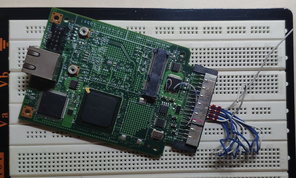
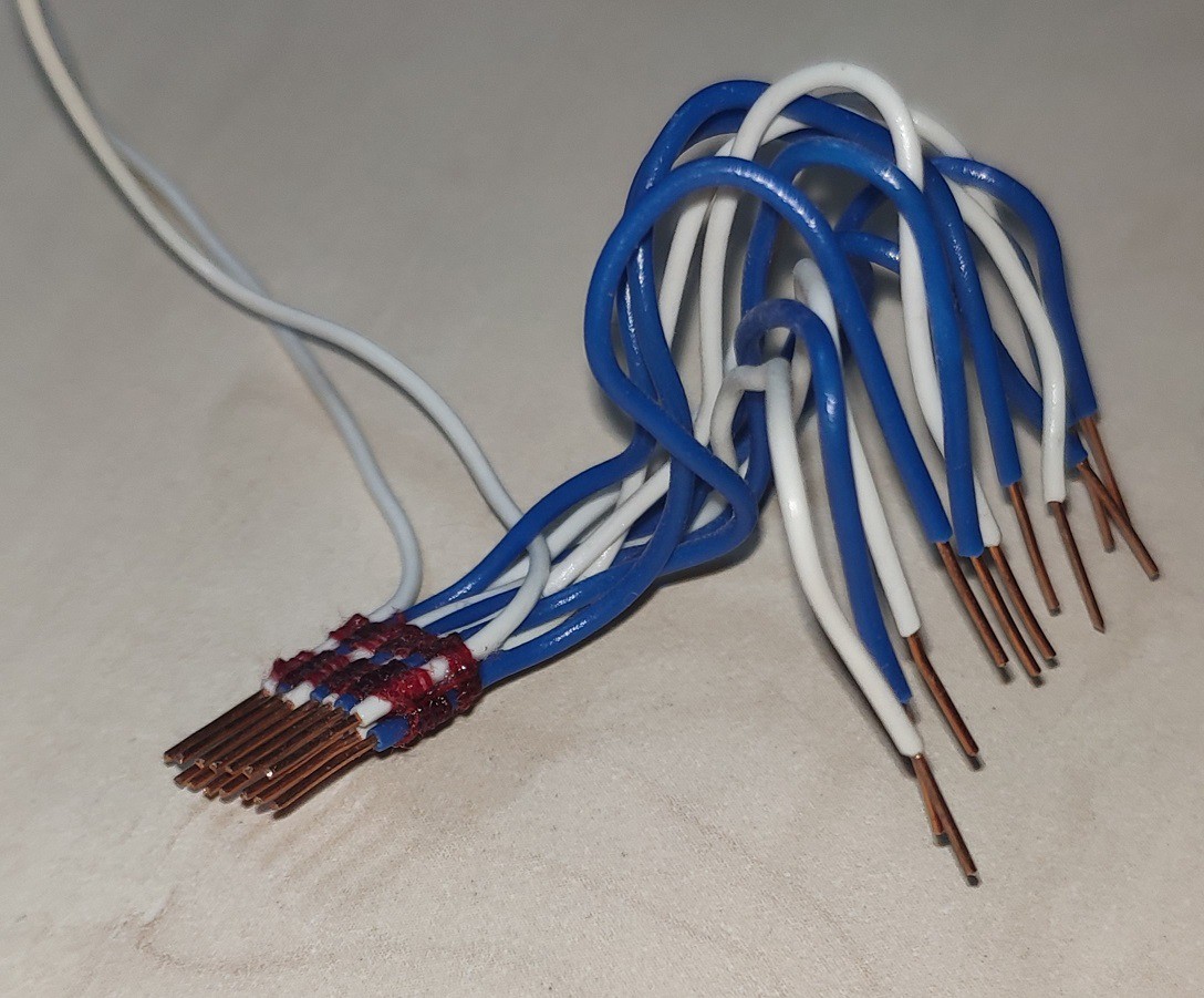
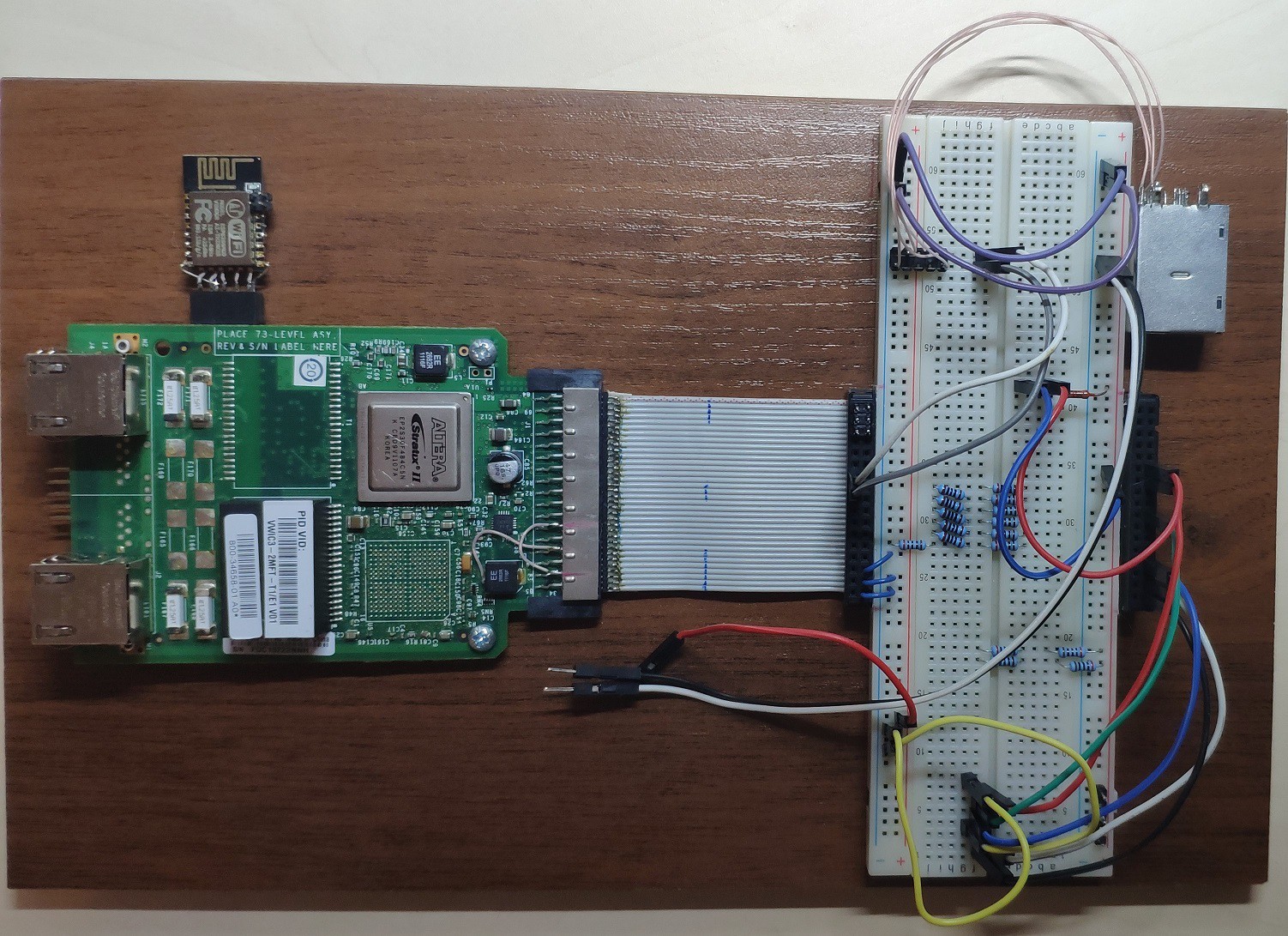
In this log there will be some of the previous versions of Breakout Boards for Cisco HWIC.
Version 1. The cheapest.


Version 2. More complicated.

A project log for FPGA Board Hack
Some components of e-waste can kill you sooner than you expect...
In this log there will be some of the previous versions of Breakout Boards for Cisco HWIC.
Version 1. The cheapest.
Version 2. More complicated.
Discussions
Become a Hackaday.io Member
Create an account to leave a comment. Already have an account? Log In.
"The only problem with this is that you now have a 5V input into pin AB17 of the FPGA (originally the enable of this LDO). The Cyclone II pins are only 5V tolerant when in PCI mode, and that's only enabled after configuration, so this might be a little bit of a problem."
I unsoldered pin 1 from the board before connecting it to pin 2 ;)
Are you sure? yes | no
I spent *hours* trying to figure out why I couldn't get JTAG to work on my VWIC3-1MFT until I figured out that !@#$!# Cisco decided to strap nTRST to GND. And then I noticed that you indeed have a patch on your board that pull nTRST to high through a detour via the USB blaster connector.
You need to document this stuff!
Any other already uncovered secret that are ahead of me? ;-)
Are you sure? yes | no
I put pull-up resistor (680 Om) only to work with my Arduino JTAG Knock-Knock board, as far as I remember Altera USB Blaster worked correctly without it.
Yes, there are:)
HWIC-3G-CDMA board contains small ICs that are marked:
U3 - VE
U7 - AN
U9 - VG
I don't think that the manufacturer is TI, it looks like Nexperia chips. I spent some time to learn more about it.
Nexperia Marking code:
First letter identifies the serie, as example: A - 74AHC, C - 74AHCT, r - 74AXP, etc.
Second letter - gate type, as example: A - 2-input NAND, B - 2-input NOR, C - inverter, etc.
As the result:
U3 - VE - Single 2-input AND gate https://assets.nexperia.com/documents/data-sheet/74LVC1G08.pdf
U7 - AN - Bus buffer/line driver; 3-state https://assets.nexperia.com/documents/data-sheet/74AHC_AHCT1G126.pdf
U9 - VG - Single 2-input OR gate https://assets.nexperia.com/documents/data-sheet/74LVC1G32.pdf
More info you can find here:
http://virtlab.occamlab.com/home/zapisnik/markuvanna-dribnoie-logiki
Are you sure? yes | no
Fantastic!
A colleague told me that it should be possible to figure out the exact functionality of the SOT23-5 chips from those letter, but I hadn’t gotten to it.
I also noticed that on the HWIC, you soldered a patch wire on that big LDO.
Outdated: My theory is that this one is used to as a power on/off switch for the PCI Express Mini card, so I haven’t looked at it yet, and the FPGA worked fine without it. Why did you add that wire?
Updated: Figured it out. It's an LDO that converts from 5V to the 3.3V of the PCI mini card. After your patch, you feed the whole card with 5V and let this LDO generate the 3.3V for you.
The only problem with this is that you now have a 5V input into pin AB17 of the FPGA (originally the enable of this LDO). The Cyclone II pins are only 5V tolerant when in PCI mode, and that's only enabled after configuration, so this might be a little bit of a problem.
Are you sure? yes | no
I've updated the section about the bitstream configuration gates with your info: https://tomverbeure.github.io/2019/11/11/Cisco-HWIC-3G-CDMA.html#bitstream-configuration.
I also added a logic analyzer to all the relevant HWIC pins and recorded the bitstream configuration sequence with a Saleae logic analyzer: https://github.com/tomverbeure/cisco-hwic-3g-cdma/tree/master/traces. The trace can be viewed with Saleae's Logic software.
Are you sure? yes | no