Blair Vidakovich
-
Parts Have Arrived
08/23/2018 at 03:39 • 0 commentsI am stuck in Perth, 4000km away from Sydney, but my girlfriend in Sydney tells me many parts have arrived.
I believe the following have all arrived
- All the resistors
- All the transistors
- All the diodes
- All the capacitors
Photos of the components will come in a couple weeks!
-
My Patreon
08/05/2018 at 17:05 • 0 commentsHello!
I have ordered all the electronic components necessary to build the flip-flops for the computer. I still have to design a good power supply, however.
I will post photos of the components when they arrive.
I will also be conducting live streams of the work sessions I do when I assemble the computer together.
I have also set up a Patreon account. If you have enough money to spare even $1 per month to help me finish this dream project of mine, I would be incredibly grateful.
This is the link to my patreon - https://www.patreon.com/dirtycommo
I have done great research for the homebrew CPU community here on Hackaday. This research includes:
This essay on DCTL logic: https://hackaday.io/project/8449/log/148234-direct-coupled-transistor-logic
This essay on DEC R-Series DTL logic: https://hackaday.io/project/8449/log/130460-bizarre-dtl-logic-levels-the-discrete-component-pdp-8And this essay on IBM's DTL Logic: https://hackaday.io/project/8449/log/131805-the-electronics-of-ibm-standard-modular-system-logic
-
Circuit Board Purchased
08/02/2018 at 08:49 • 0 commentsI do not have the budget to fabricate fibreglass PCBs, so I must either hand solder veroboard or perfboard.
Veroboard and perboard is very expensive at good qualities, and cheap board is of terrible quality and structural integrity.
So, to keep costs down, I turned to re-using waste.I am going to use acrylic board (PMMA acrylic) I obtained from the Sydney Marrickville Reverse Garbage centre. It was very cheap, at $18 for approximately 3 metres squared.
Drilling holes in the plastic will be time consuming, so I will superglue surface mount components to it, and hand solder them once they are attached.
SMD construction will be more time efficient and will reduce the size of the computer.
I believe that the plastic can be cut or snapped into ''flip chips''.
I am open to fabricating ''flip chips'' for others on a not for profit basis.
The next step is building the power supply and ordering the components.
![]()
-
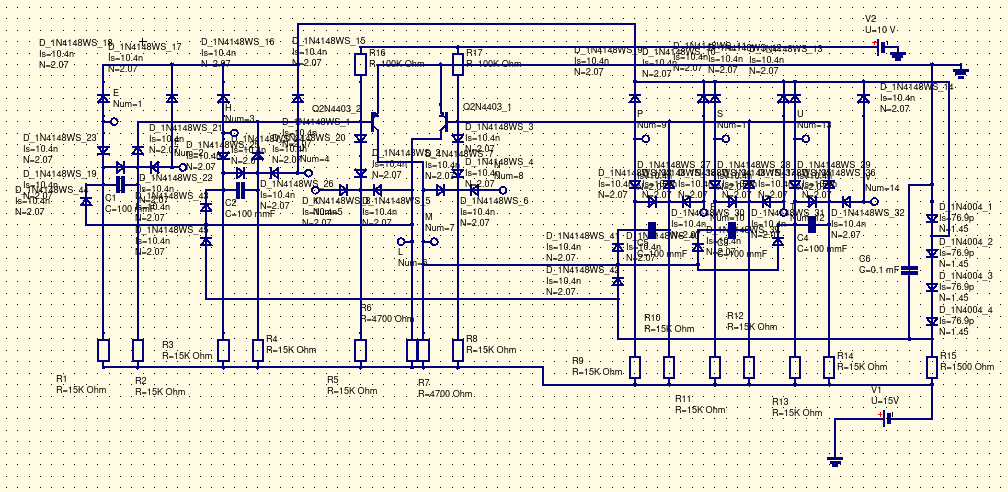
Explaining The R-Series Logic Flip-Flop
07/27/2018 at 16:01 • 0 commentsI received some constructive criticism about the Flip-Flops I am using the construct the various elements of the RAVEN. I think a lot of the apprehension other hackers have about the R201 DEC Flip-Flop I am using is because it contains a great number of circuit elements -- if these circuit elements were in a large part active during Flip-Flop operation, then obviously the R201 would be very slow.
In this log I'd like to clean up and and explain exactly how the main Flip-Flops in the RAVEN will function. I do not believe these DTL Flip-Flops I have lifted from DEC R-Series Logic are slow, and will result in less than 1 MHz performance.
The Most Basic Element of R-Series DTL Logic
The most basic circuit element of any electronic digital logic is the inverter. This is the basic inverter of the DTL logic that the RAVEN uses:
![]() A couple of examples can be provided which show the actual way this inverter is implemented in R-Series Flip-Chips:
A couple of examples can be provided which show the actual way this inverter is implemented in R-Series Flip-Chips:The R113 Diode Gate
![]()
The R121 NAND Gate
![]()
R-Series digital logic specifies -3V as logical ONE, and 0V/Ground as logical ZERO.Inverter Simulation
Conventional current flows up through the emitter of the transistor, and out through the collector. Depending on whether there is 0V/ZERO or -3V/ONE at the INPUT terminal determines whether current will flow out through the base of the transistor and cause it to saturate.
-3V/ONE at the INPUT terminal will reverse bias the INPUT terminal diode, and open up a path for current through the transistor base up through the -15V terminal past the steering diodes. The transistor will then conduct, and the voltage at the output terminal will be 0V/ZERO, effecting an inversion.
0V/ZERO at the input terminal will cause the INPUT terminal diode to become forward biased, making the current path through the transistor base a path of much higher resistance. A small amount of current still leaks through the base through to the -15V terminal near the INPUT, but it is not enough to turn the transistor on. The transistor stops conducting and the voltage at the output terminal is therefore -3V.
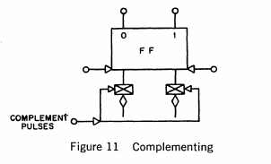
R-Series Logic Flip-Flops
The simplest Flip-Flop of the RAVEN is two Inverters complementarily connected together like so:
![]()
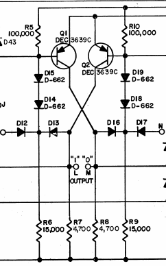
As you can see, this is the heart of the R201 Flip-Chip:
![]()
What, then, is the rest of the circuitry in this schematic?
Diode-Capacitor-Diode Gates
The answer is that the extra circuitry is 'Diode-Capacitor-Diode' gates. This circuit element is a very innovative and useful solution for both (a) edge-triggering; and (b) constructing JK and D Flip-Flops is as little circuitry as possible.
This is the basic DCD gate:
![]()
The basic principle behind this circuit is that the capacitor charges and remains charged so long as the PULSE INPUT is held at -3V, and the LEVEL INPUT is held at 0V.
When the LEVEL INPUT equals 0V, and the positive edge of a PULSE INPUT signal changes from -3V to 0V, a positive voltage is generated at the output, which serves as a trigger for a Flip-Flop.
When LEVEL INPUT = -3V and PULSE INPUT changes from -3V to 0V, no such positive pulse is produced.
See the following simulation:
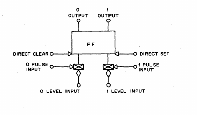
Creating D and JK Flip-Flops
The process of creating complex, clocked, edge-triggered Flip-Flops is as simple as preparing the inputs to Flip-Flops attached to DCD gates. The following two schematics are isomorphic/identical in meaning:
![]()
![]()
A JK Flip-Flop can be constructed by simply sending identical pulse inputs to a DCD-gated Flip-Flop:
![]()
So long as the LEVEL INPUTS are tied to ground, identical PULSE INPUTS will cause a Flip-Flop to complement.
This simulation demonstrates a JK Flip-Flop constructed from a DCD-gated Flip-Flop:
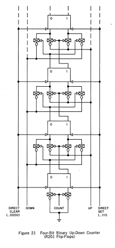
This serves as the basis for this Up-Down Binary Counter Register:
![]()
Binary counting is therefore achieved with the minimum number of circuit elements, as well as minimum number of transistors!
The exciting thing about DCD gates is that they allow logical isolation - meaning one does not need to resort to using Master-Slave Flip-Flops in order to clock some Flip-Flop element. Logical isolation from input and output is achieved by DCD gates, which allows the component count to be reduced dramatically.
-
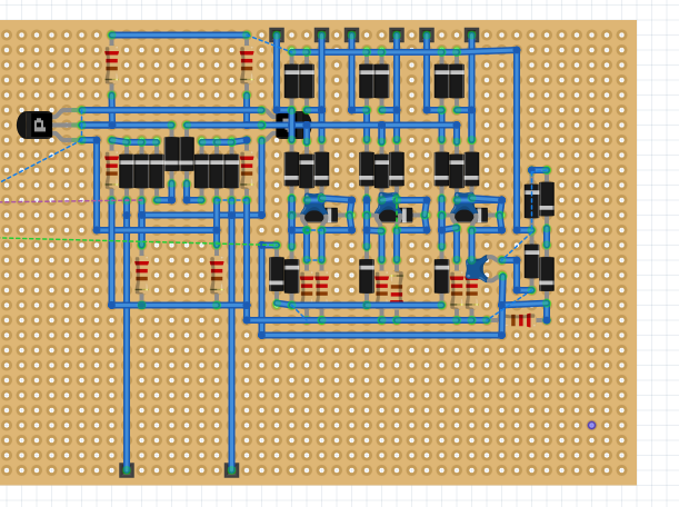
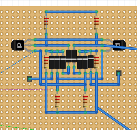
R201 Flip-Flop Perfboard Layout #2
07/23/2018 at 09:21 • 0 commentsThis is half the Flip-Flop completed. It is the entire right side of the R201 specification. It now includes that actual Flip-Flop, and the 3 edge-triggered inputs on the right hand side of the design, including the voltage divider.
![]()
This layout corresponds to this fraction of the R201 schematic:
![]()
-
Designing The Perfboard Layout #1
07/23/2018 at 08:05 • 0 commentsI do not have the budget to get printed circuit boards made, so I am using some software called Fritzing (link) to do the layout of the components on perfboard.
This is the heart of the R201 Flip-Flop completed:
![]()
This layout corresponds to the following section of the R201 schematic:
![]()
It is by far cheaper for me to solder a great many of these perboards by hand, instead of etching or paying for the manufacture of PCBs.
I will hopefully have another update tonight.
-
Creating Virtual Schematics Using Qucs
07/22/2018 at 03:32 • 0 commentsI will be using the Free Software program Qucs to plan out the electronics of the RAVEN.
The digital electronics of this computer will be based on the R-Series logic of the DEC PDP-8/S.
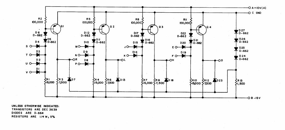
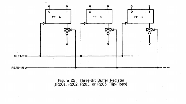
I started planning out the registers of the RAVEN, following this 'cookbook' suggestion inside the 1967 DEC Logic Handbook:
![]()
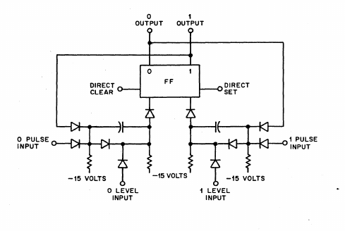
The DIRECT SET lines will not be tied together, and they will not be unbuffered. The DIRECT SET lines will have a three state input implemented with an extra R-Series Diode-Capacitor-Diode Gate attached to each separated DIRECT SET line:
![]()
So the extra 'CLEAR MDR' control signal will be implemented by attaching all DIRECT CLEAR lines together. This will be useful for the CLEAR STACK CELL control signal/sequence.
Flip-Flops Required for Registers
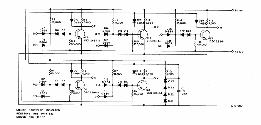
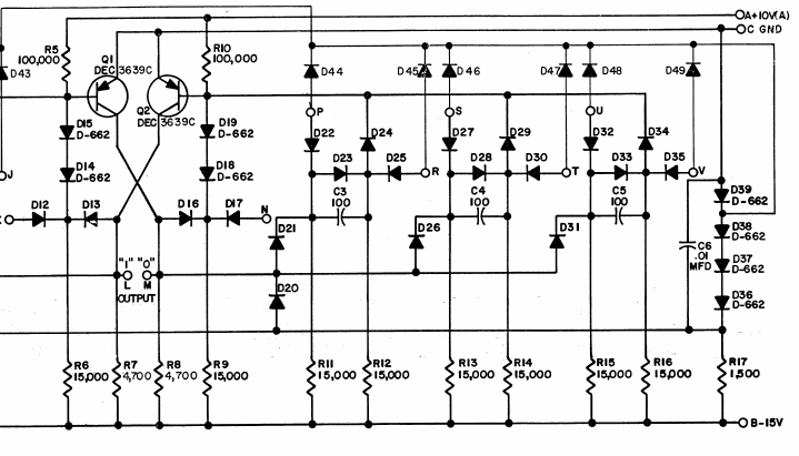
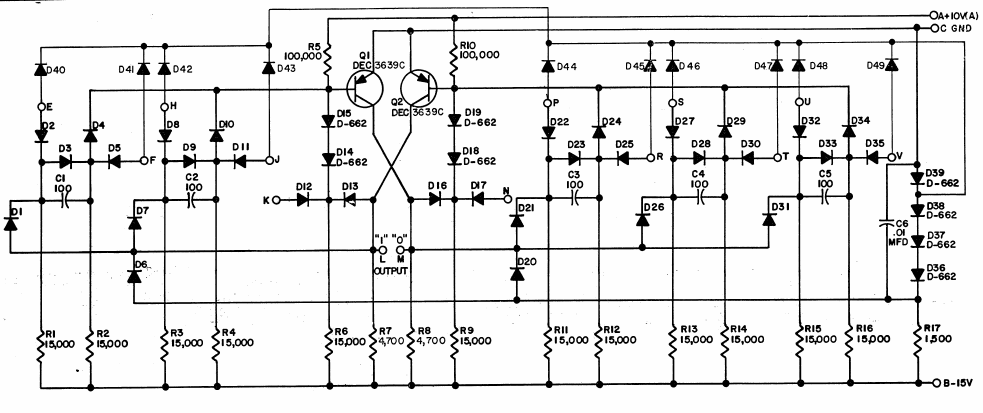
This is a 5-input single Flip-Flop as specified by DEC Flip-Chip code R201:
![]()
And this is the corresponding circuit schematic in Qucs:
![]()
And this is the sub-circuit schematic that is generated by attaching ports to the appropriate inputs and outputs:
![]()
Now the registers can be designed (and hopefully simulated) in Qucs and an accurate Bill of Materials can be generated.
-
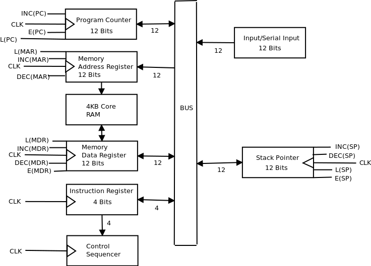
Log #1 - Designing the Data Flow
07/22/2018 at 03:13 • 0 commentsThis is the first attempt at a data flow diagram of the RAVEN. I spent a lot of time researching and analysing the MENTAL-1 computer built by Trey Keown here on Hackaday.io. That computer was built with TTL logic. It implemented a simple but slow 'SCAN' control signal which decremented the Program Counter to a corresponding [ instruction after executing a ] instruction.
After reading the discussion that Trey conducted on reddit, and seeing that he suggested implementing a stack pointer register in order to speed up the [ and ] looping process in brainfuck code, I decided to come up with a CPU architecture based on the PDP-8/S and Malvino SAP-2 that implemented a stack pointer.
This is the rough idea I have for the CPU architecture data flow for the RAVEN, after looking at the PDP-8/S and SAP-2:
![]()
The CPU does not require an accumulator, or temporary buffer registers, because the only data manipulation that the brainfuck instruction set implements is incrementing and decrementing memory cells ("memory locations", "memory words").
So in order to implement the instructions +, -, and < and >, all that is required is control signals from the control sequencer that increment and decrement the MAR and MDR.
The MAR
The MAR is not a bidirectional/three state register. After it receives a memory location from the PC, or is cleared to $0000, or increments or decrements itself, it always holds the address locations to which it points in the core memory HIGH.
Currently I do not want to implement ROM memory, I will implement a tape reader like Yann Guidon's optical-based reader. I haven't checked out how the PDP-8 loaded in programs. I envisage loading programs will be a lot like bootstrapping and running something like an Altair 8800.
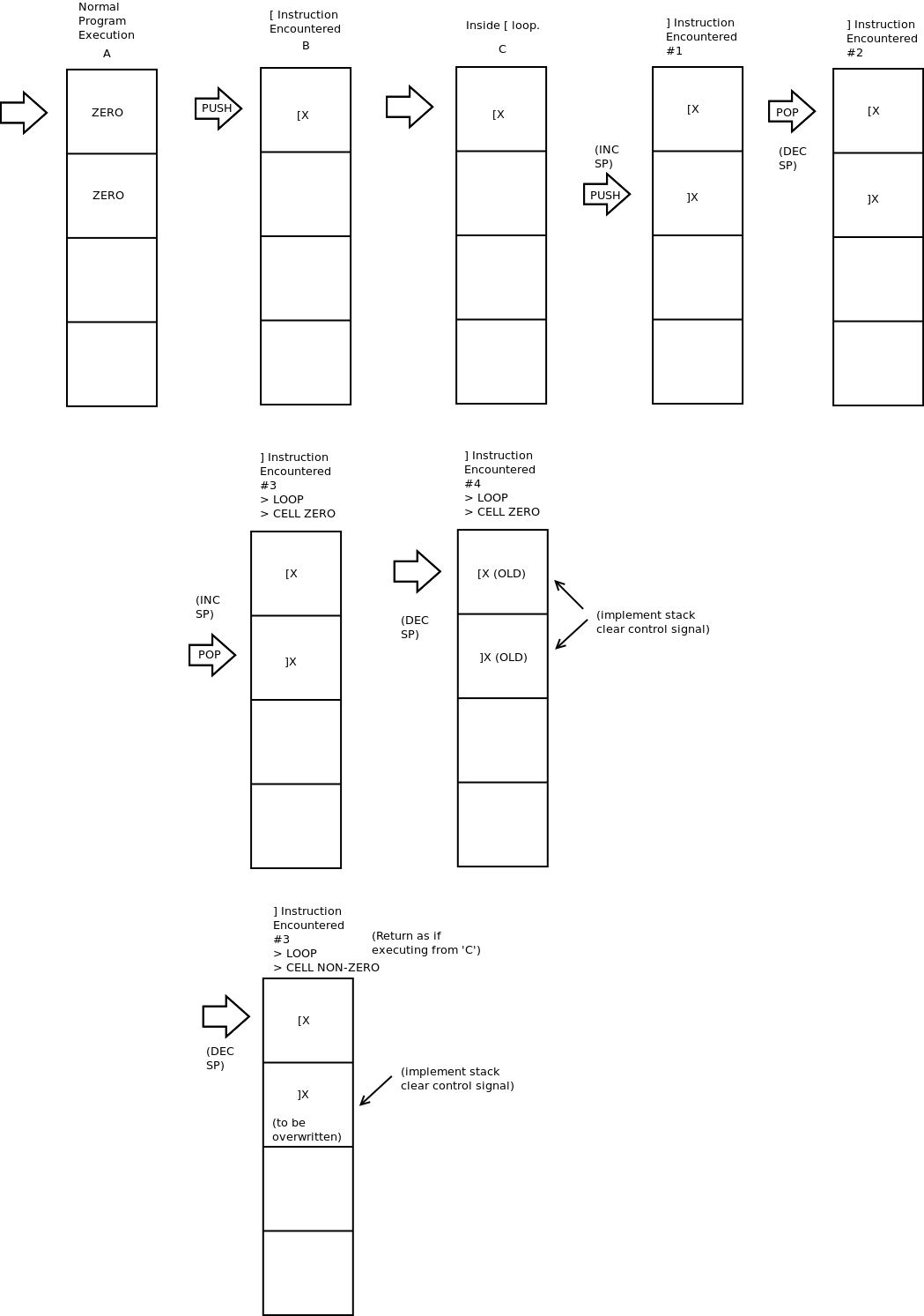
The Stack Pointer; [ and ] instructions
The SP will be able to be initialised anywhere in memory, but from my time with 6502 Assembly, I would recommend somethere like $XXFF. Instead of a [ instruction incrementing a SCAN counter register like in MENTAL-1, [ will:
- test to see if the current stack location is non-zero
- if non-zero, increment the stack pointer
- then push the next Program Counter (PC) state onto the stack (the memory cell after a [ command is the loop counter),
- and then continue execution.
When a ] instruction is executed,
- the stack pointer is incremented,
- and the PC state after the ] instruction is pushed onto the stack.
- Then, the stack pointer is decremented
- and the PC state of the loop counter cell is popped off the stack and loaded into the PC.
- The MAR is then loaded with the memory cell location,
- and the data is loaded into the MDR.
- If the cell is data equals zero (I need to implement a flags register linked to the MDR), the stack pointer is incremented
- and the state after the ] instruction is popped from the stack and loaded into the PC,
- the stack pointer is then decremented to cause the old [ location to be overwritten, and execution continues.
- I think it would probably be wise implement a 'stack clear' operation to write $0000 to the old [ location. This would just require loading the MDR with ZERO, and then writing that to the SP memory address.
BUT
- If the loop counter cell is non-zero, the old ] location is written with ZERO,
- and the stack pointer decremented and execution continues.
The organisation of the stack will look like this, as [ and ] are executed:
![]()
R.A.V.E.N. -- A Transistorised Brainfuck Computer
[R]eduction to [A]lgorithms of [V]ersatile [E]soteric m[N]eumonics

 A couple of examples can be provided which show the actual way this inverter is implemented in R-Series Flip-Chips: