Hello there,
The used Akai MPC 2000 pads arrived this morning, yay!
I took the opportunity to share with you actual dimensions of the pads, as well as some photos of the inner guts of this prototype; let's start with the description of the electronics photos:
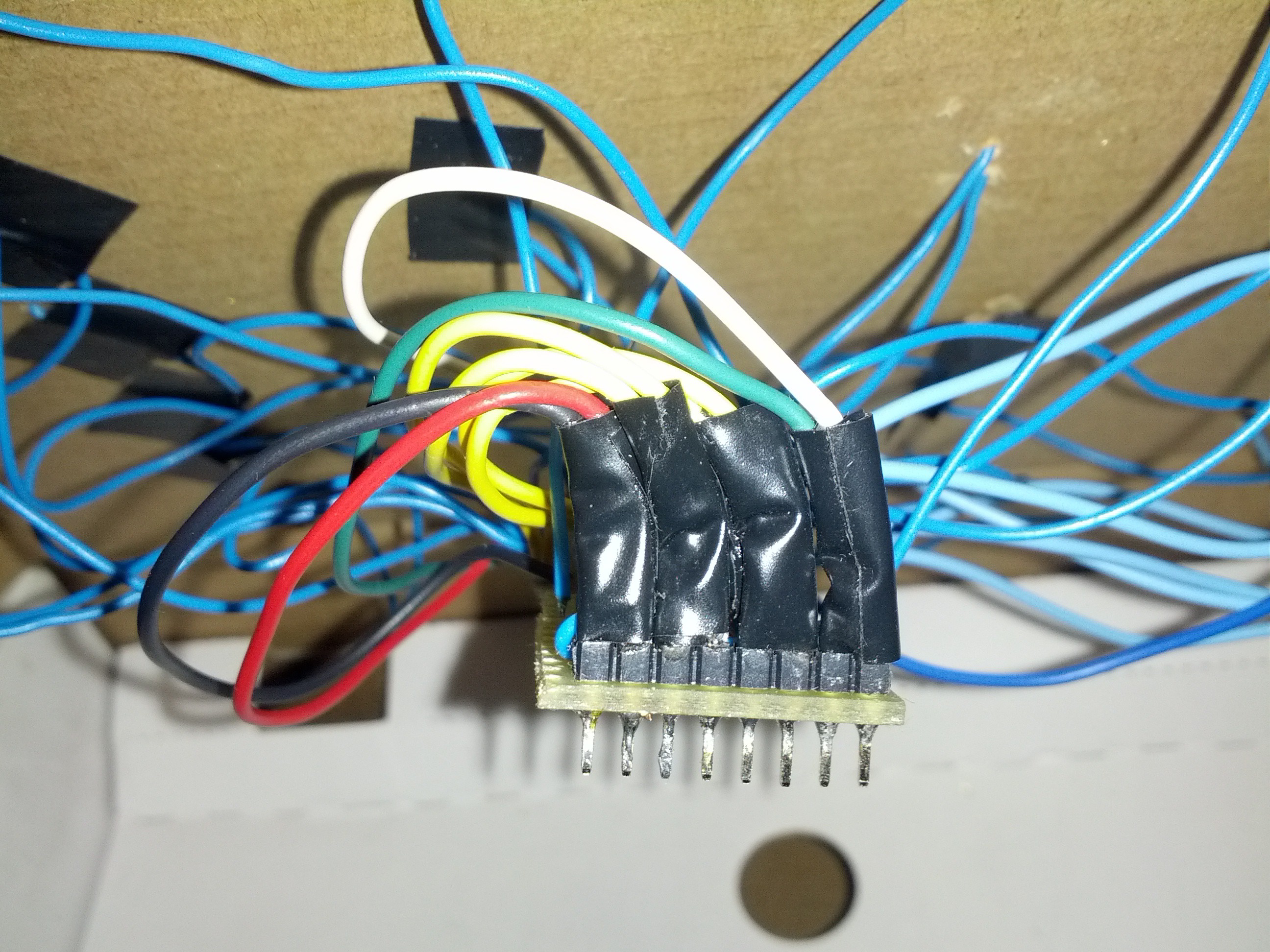
This is the mux breakout board connector; beside the blue wires mess, which is composed of the FSRs leads, you can see in order from left to right, and color coded:
Vss (ground)- Vdd (5 V) - A - B - C - D - Common Out - Inhibit
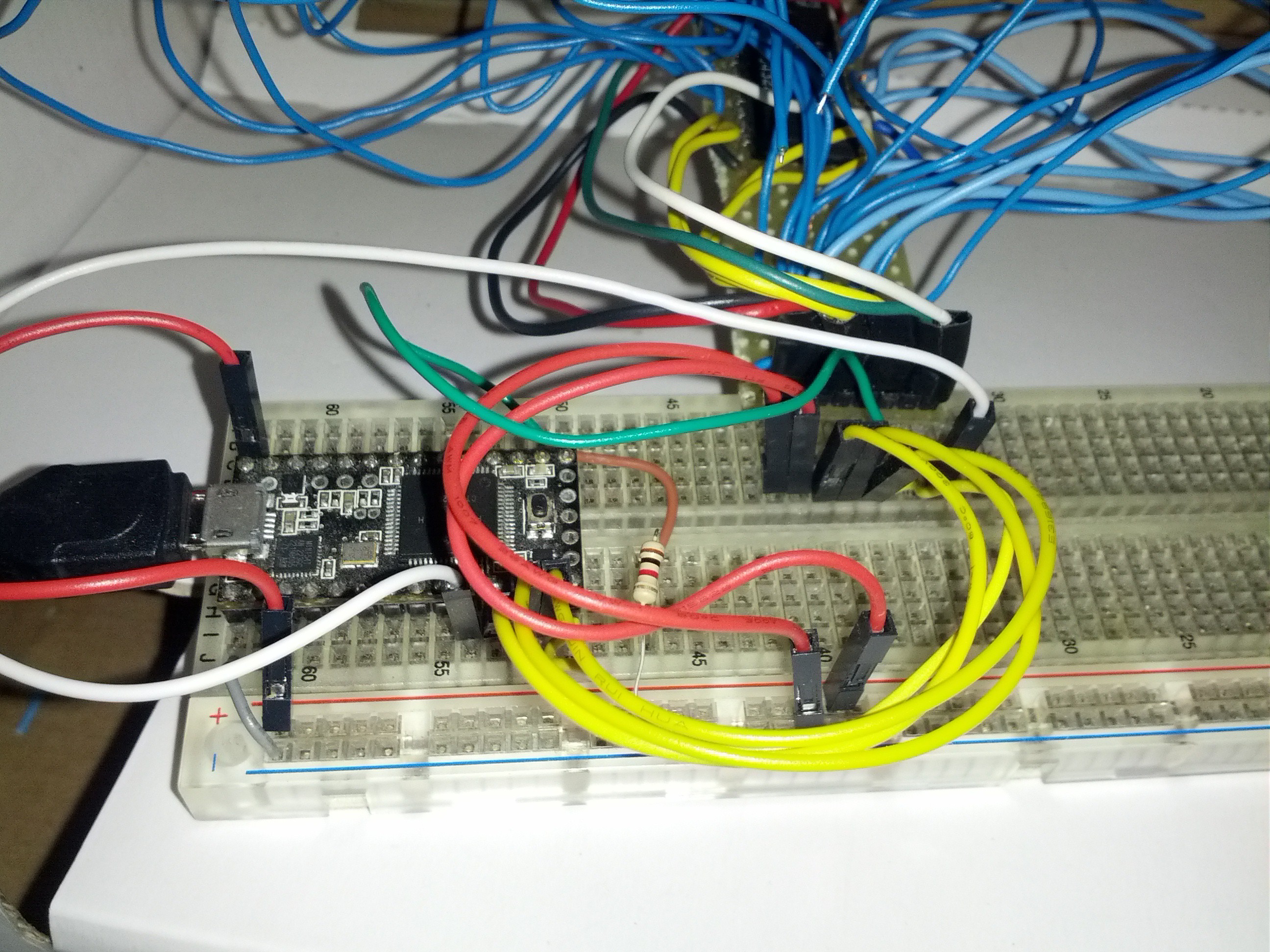
This board is plugged in a breadboard and connected to the Teensy using some jumpers:
You can see that apart from the red jumper for the ground connection, everything follows the same color coding as on the breakout board:
RED for Power - YELLOW for A-B-C-D - GREEN for Common Out - WHITE for Inhibit
A-B-C-D are connected to pins 9-10-11-12, Inhibit to pin 8, Common Out to A0-pin 14 and grounded through a 10 Kohm resistor. You can see that the electronics and the connections are really straightforward.
Now for the dimensions:
- Top layer:
. Pad width : 1,1875 inches
. Spacer between pads : 0,1875 inches
These could be approximated to 1,25 inches and 0.125 inches and will be useful later when designing the final enclosure (e.g. to cut an acrylic sheet with some holes to be put on top of the pads to keep them together with the structure, which will also make the thing look sleek ;D )
- Bottom layer:
. Pad width : 1,25 inches
. Spacer between pads : 0,25 inches
. "Pressure" circle diameter : 1 inches
For "pressure" circle I mean the little convex circles under each pad, which will be covered with Velostat;
The width and the spacer reflects the approximated top pad dimensions; these are necessary to design the PCB pads.
I made some math, and the first thing that comes out is that I cannot fit 16 pads in a single PCB, at least not in Eagle CAD; the maximum available area in the free version is 100 mm * 80 mm ( 4 inches * 3,2 inches ), therefore I have to either stick with 4 boards with 2x2 pads each ( 3 * 3 inches ), or design these with another tool.
You can find more pictures in the Google Drive shared project folder link.
See you next time with the PCB layout of the pads, and who knows what else!
Stay tuned,
Mick
 Michele Perla

Discussions
Become a Hackaday.io Member
Create an account to leave a comment. Already have an account? Log In.
I registered to follow this project only. Looks like your pads are really responsive, unlike on real AKAI controllers.
Good luck, i´ll follow your steps closely ;)
Are you sure? yes | no