EDIT: the final, completed in hardware, version of ALU described in newer post.
Original:
This is the description of the Arithmetic-logic unit of this "computer".
Most of it I conceived a year ago, and now, after some modifications, it is one of the most stable parts of the system (along with the register file).
Here is it's inner organisation:
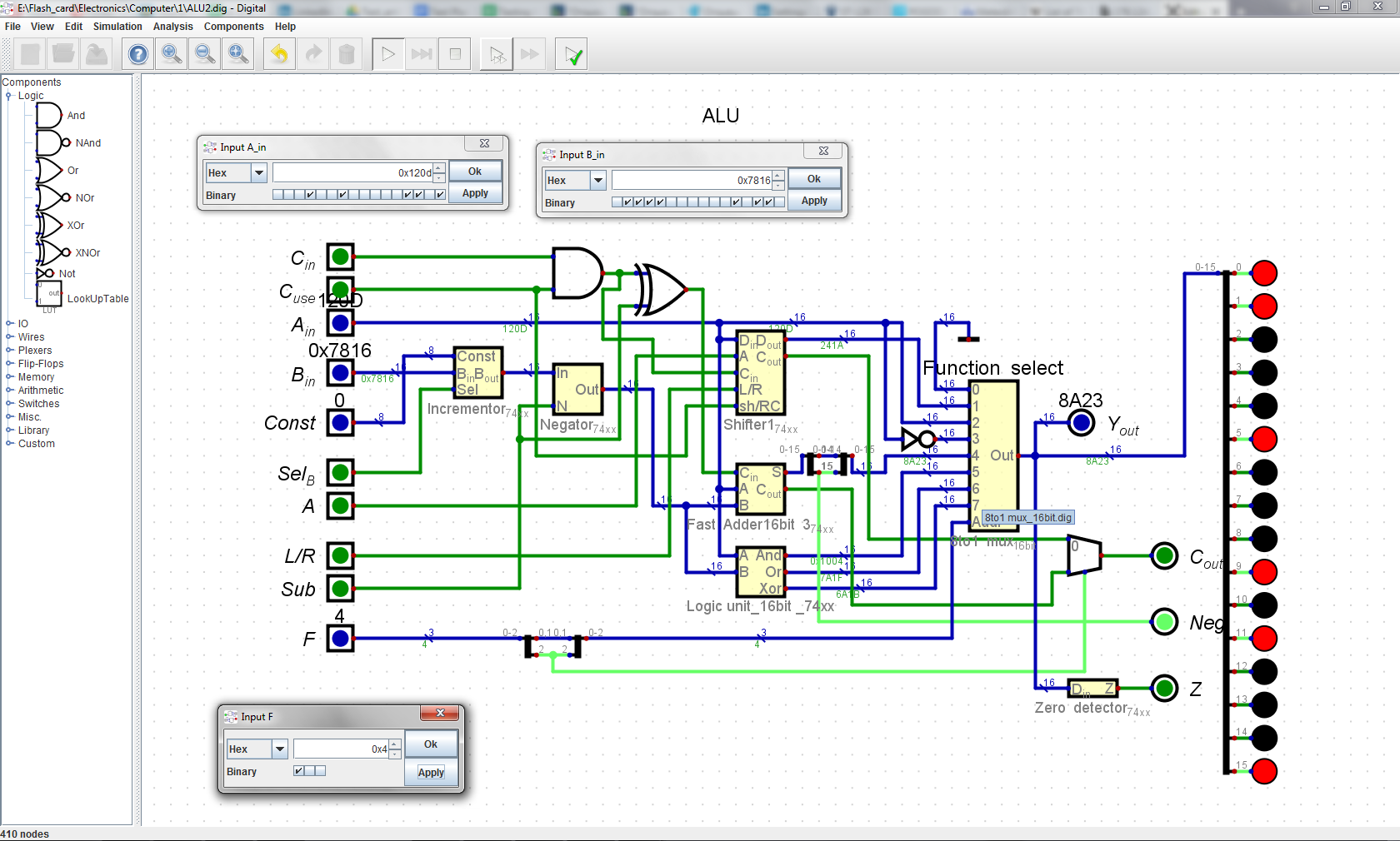
The ALU accepts two 16-bit operands, A_in and B_in, and outputs one 16-bit value, Y_out, which for ease of debugging is also outputted to 16 LEDs on this schematic.
The A_in and B_in are supplied from Register File, but there is possibility of substituting B_in with some constant value in the range 0 to 255, that is suplied through Const input. Selecting of what is going as B operand is accomplished by 1-bit control line Sel_B through the Incrementor module (just 2-to-1 mux).
Next, the B operand is going through the Negator module (16 parallel XOR gates), where 1-bit control line Sub dictates if B will go further unchanged, or all its bits will be flipped. This same line flips carry bit that goes into adder for facilitating subtraction in twos complement.
On the next stage there are several blocks in parallel, namely, Shifter, Fast Adder and Logic unit.
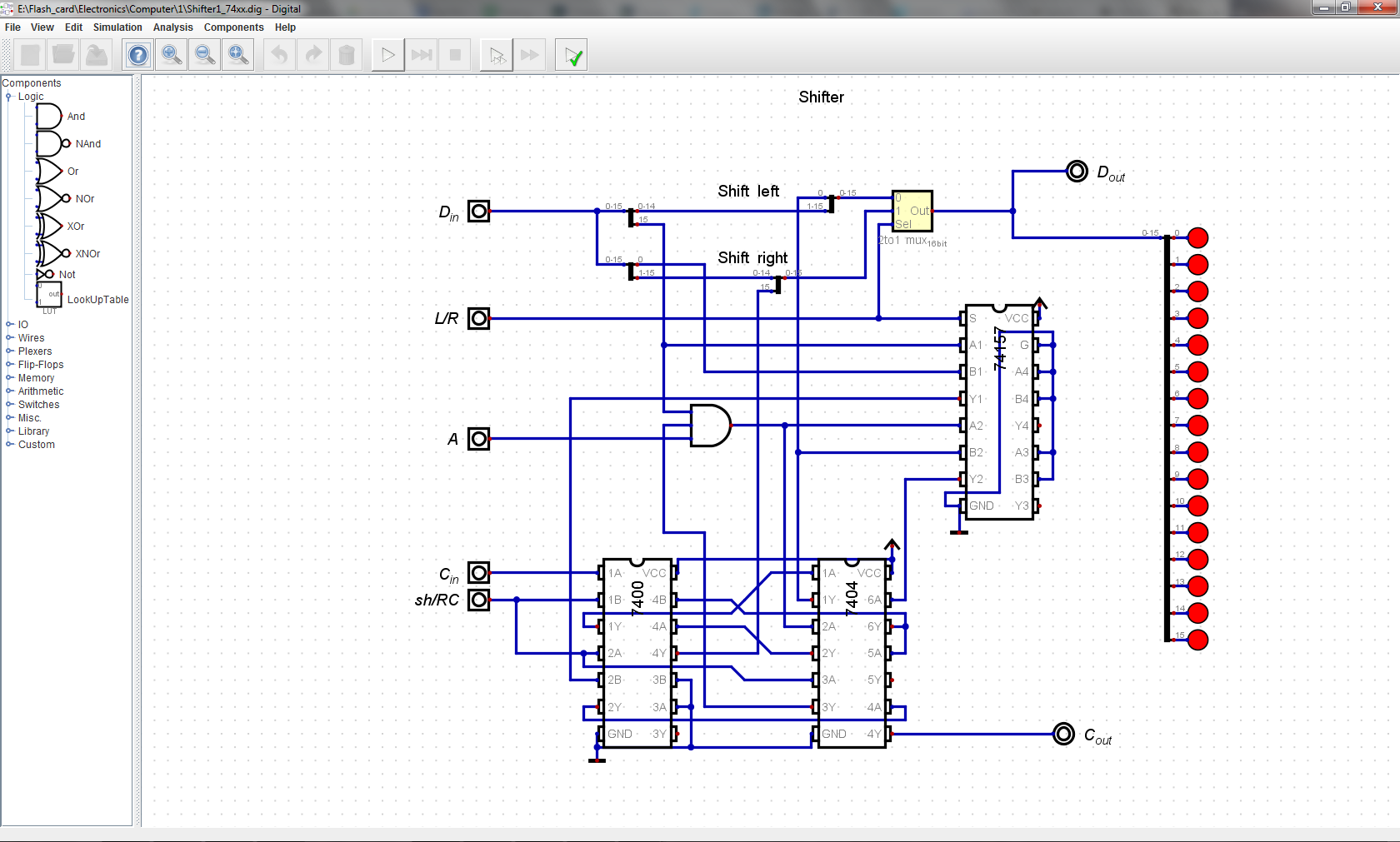
The Shifter works only on A_in operand, so it is ignores whatever is B value. This module takes in 16 bit D_in and 1 bit C_in (carry in) and outputs 16 bit D_out and 1 bit carry out. The three controls are: A - for Arithmetic shift, L/R - for choosing shift direction, and sh/RC, for choosing between Shift and Rotate through carry. The Shifter mostly consists of 2-to-1 muxes with handful of logic gates.
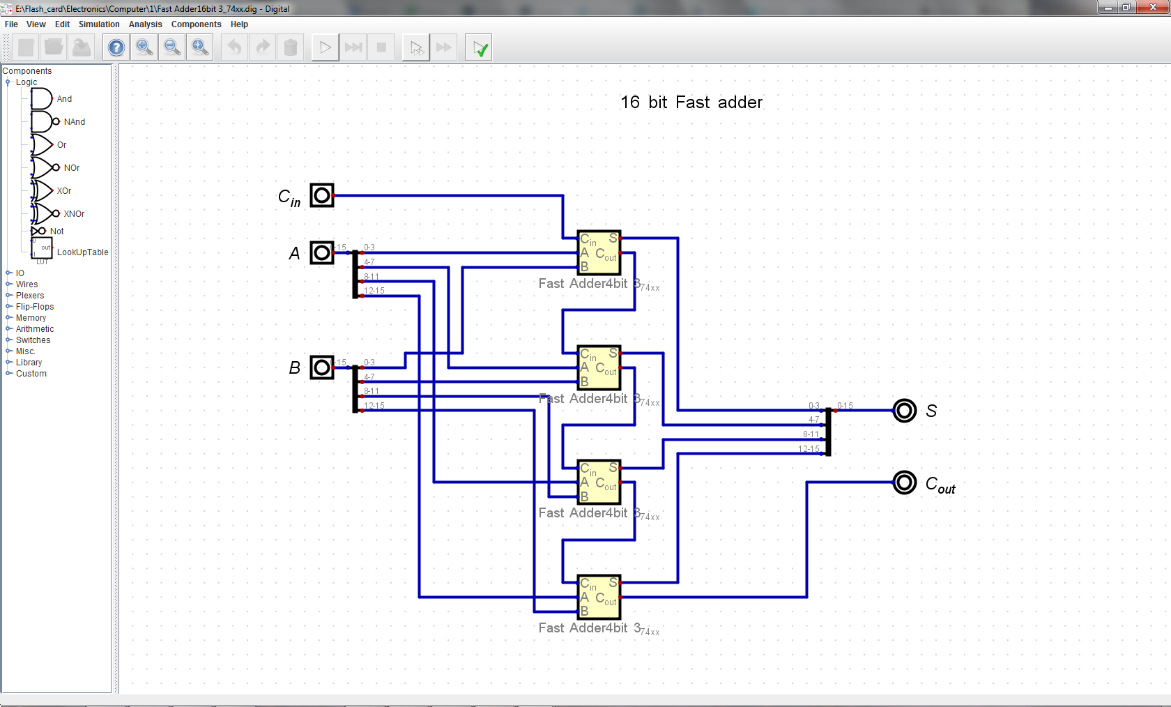
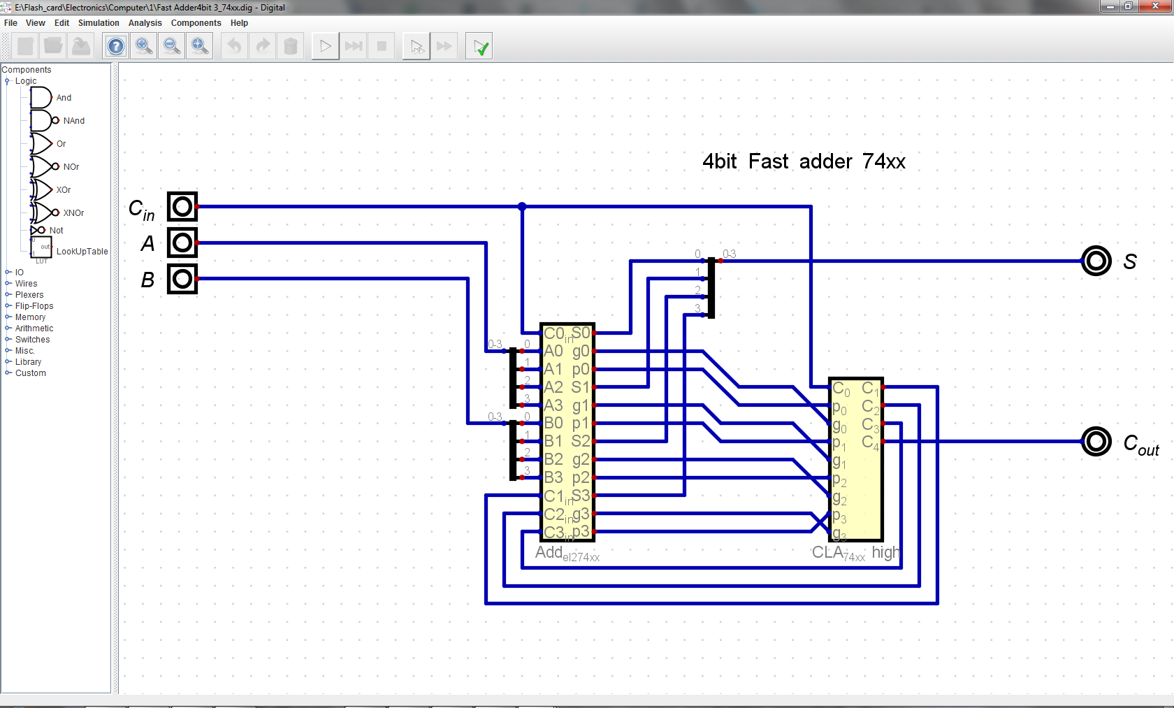
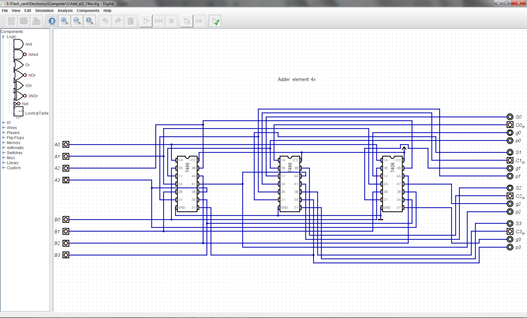
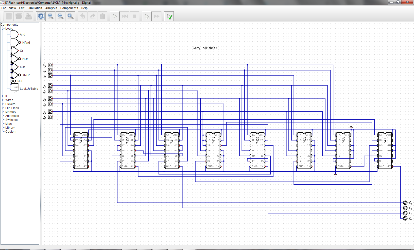
Fast adder takes in C_in, A_in and B, outputs S and C_out. It is comprised of four chained 4-bit fast adder units. Constructed from simple logic gates throughout, no fancy 74181/2/3 chips.
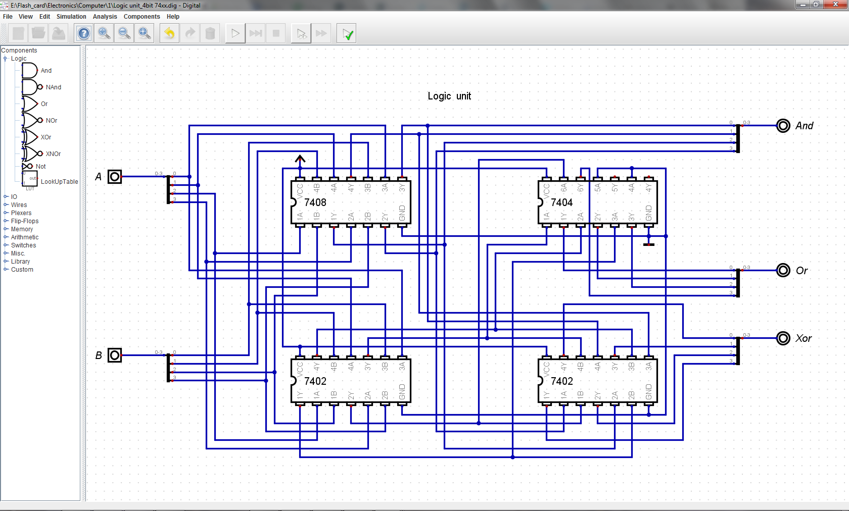
Logic unit also operates on A_in and B_in inputs bitwise, has three outputs. Essentially, it is compound XOR gate ( made from ANDs and NORs + inverters), so AND, OR and XOR are achieved in the same circuit.
The last stage is the big 8-to-1 16 bit mux, which is controlled by 3-bit F (as in Function) control line. It chooses which function result will be output from the ALU.
Here are these functions:
000 Zero -- no matter what inputs, all bits are set to '0' output
001 A shifted -- whatever comes from the Shifter unit (itself controlled by A, L/r and sh/RC lines) -- could be SHL, SHR, ASHR, ROLC, RORC
010 A -- A_in goes straight through to the output
011 ~A -- A_in gets inverted
100 ADD (A,B) -- result from adder, can be any of the ADD, SUB, ADDC, SUBC
101 AND (A,B)
110 OR (A,B)
111 XOR (A,B)
In total, this ALU is capable of 28 different operations, though in many cases some of the operations can give the same result.
 Pavel
Pavel
Discussions
Become a Hackaday.io Member
Create an account to leave a comment. Already have an account? Log In.
ok, thanks.
Are you sure? yes | no
hello, this is great!
is this a good design for a FPGA (gates logic boards), or better for discrete logic?
Are you sure? yes | no
I have no idea, really.
The project is intended for building with 74hcXX logic chips.
I am not proficient in hardware description languages and have no tools for working with FPGAs.
Are you sure? yes | no