There are several 8-to-1 and 4-to-1 multiplexers around the build, which are routing 16-bit and 32-bit wide signals. Managing all this wiring looks like a challenge (one have to look at the Pilot-1 CPU, which is mostly a register file coupled with ALU -- it is ribbon cables all around.
There are quite a lot of wires criss-crossing the 8-to-1 multiplexer boards. It helps that these wires are all individual, and 3-d space allows to weave them as one pleases.
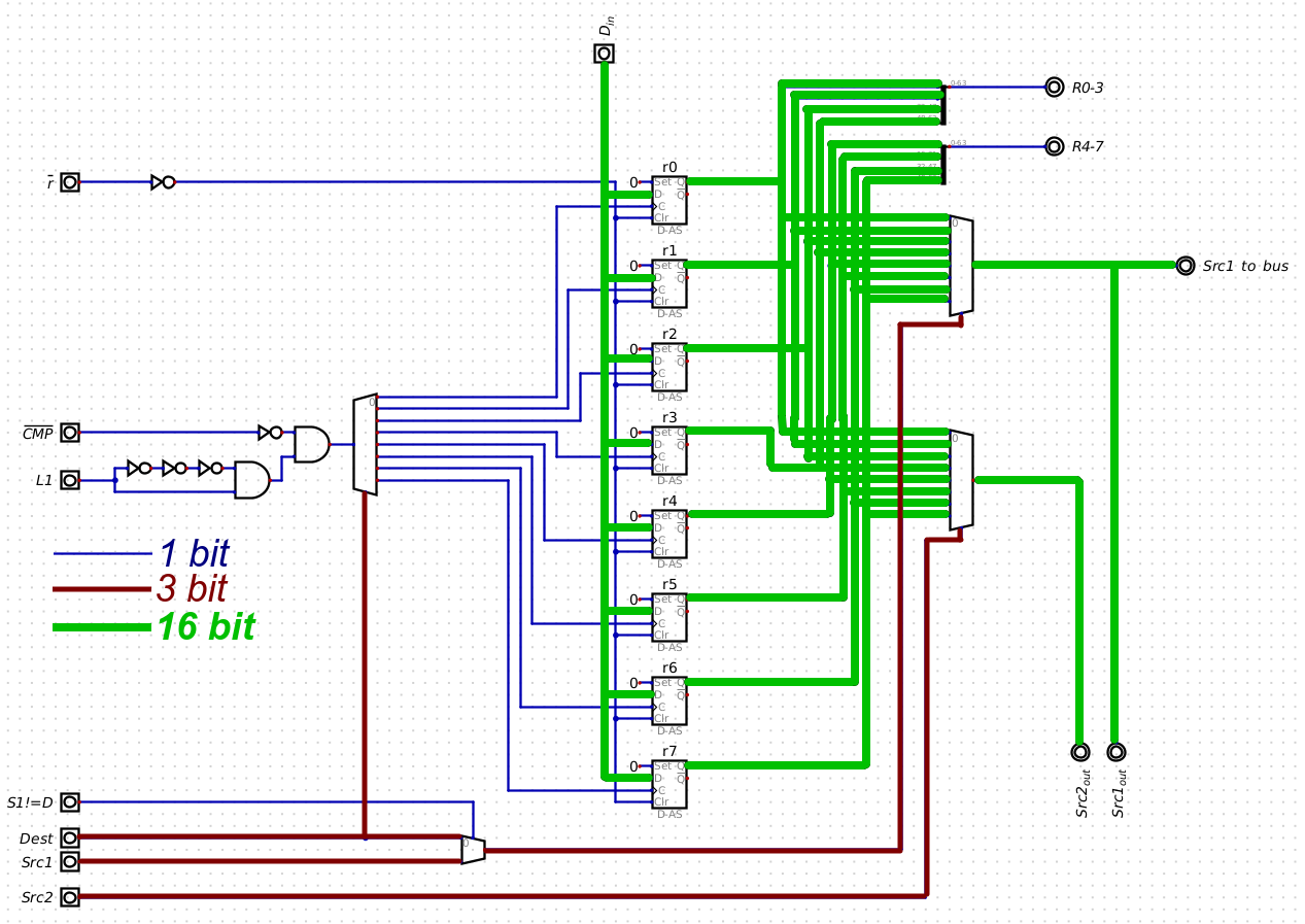
Here is the example schematics for Register File, there are a LOT of 16-bit paths:

If I to replicate such structure on PCB, turning these wires into traces on 2 planes, it seems that there will not be enough space, and I'll need multi-layered PCBs which are more complicated and expensive to order, and if there some wiring bug in buried layers, there is no way to repair it.
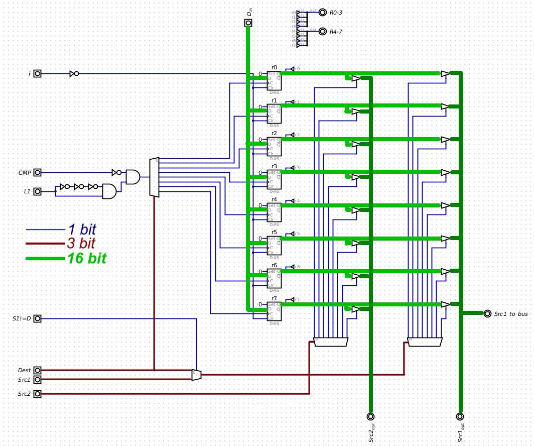
The better solution, it seems, would be to replace multiplexers with tri-state buffers that feed into common bus and activated by single 3-to-8 decoder. This must greatly simplify the build.
Revised schematics for Register File, using tri-state buffers, it looks much more manageable:

This new solution will be applied for replacing 4-to-1 and 8-to-1 multiplexers; the 2-to-1 multiplexers are fine as they are, wiring them is not as complicated. This replacement will cut greatly into the number of ribbon cables and weird orthogonal board connections in the final build.
The reason I was vary of using this solution earlier is that I thought it would be significantly slower. But it applies more to situations where the clock speeds are much higher and there are much more such outputs to single bus. In my case this speed penalty looks insignificant.
Also, when actually looking into datasheets, the propagation delays for 8-to-1 multiplexer and tri-state buffer are almost the same, and my worries were unsubstantiated.
 Pavel
Pavel
Discussions
Become a Hackaday.io Member
Create an account to leave a comment. Already have an account? Log In.