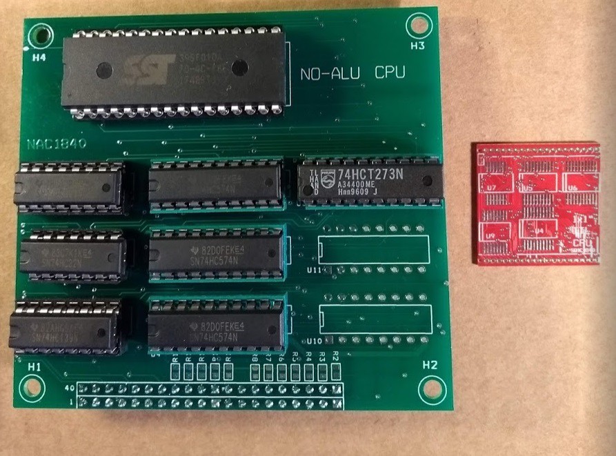
The NAC pcb is a bigger version of the square inch pcb. It is intended to make debugging easier. It has two unused footprints, to have room for extra IC's if that would be needed.:

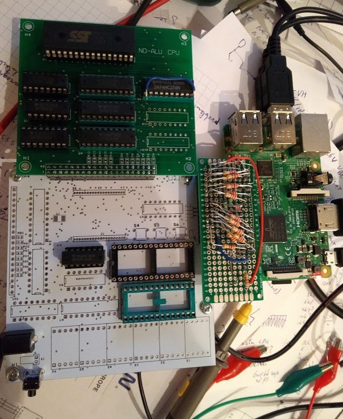
Debugging started with the NAC connected to the application pcb and the Raspbery Pi programmer.
The Raspberry Pi will have two python scripts, one for programming the microcode and one for programming the application code. The last one can also single-step the processor and display the micro-instructions and databus value at each step.

I corrected a few problems. At this moment, stepping through the microcode works, but only for about 6 micro-instructions after reset. After that, microcode reads as FF... have to investigate....
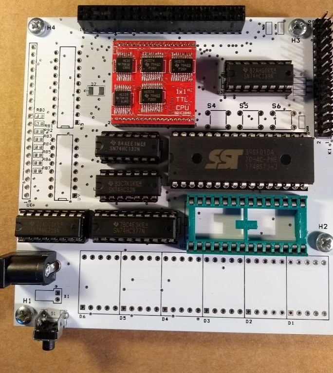
Next picture shows the square inch cpu on the white application pcb. The application pcb contains RAM (empty socket on picture), Flash-ROM, I/O and support functions like clock generation, reset circuit and connecting to the RPi programmer:

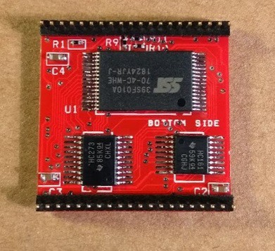
And here is the backside of the CPU, with the 'big' microcode Flash:

Discussions
Become a Hackaday.io Member
Create an account to leave a comment. Already have an account? Log In.
This is looking awesome!
Are you sure? yes | no