Yay! The schematic is not that complicated, it took me longer to create all the symbols and footprints!
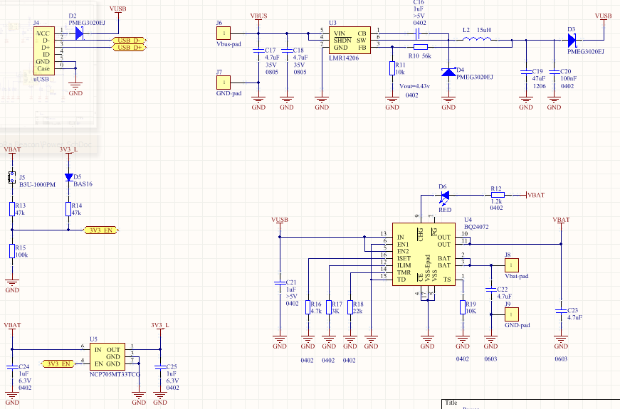
Each block has its own schematic page. Let's start with the power block:

- J4 is the micro-USB connector. The diode makes sure there is no reverse current in case of powering the locator via the step-down converter and the USB cable is attached to a shut-down device. Perhaps nothing happens, but you can never know... USBD+ and USBD- ports connect to the MCU.
- Power for the buck converter comes from two pads. The output of the LMR14206 is also isolated through a diode, to prevent reverse current.
- The NCP705 is straight-forward: 1uF input and output capacitor and a direct conection to the MCU for Enable.
- The BQ24072's input current is limited at ~500mA using the 3K resistor (R17). The charge current is set by R16 at ~200mA. I limited the input current at 500mA because the charger can power the circuit and charge the battery at the same time. I intend to use a 200mAh Lipo cell (so 1C charge rate). The rest of 300mA are reserved for the load: 120mA for the LoRa TX burst, and 55mA for the GPS module. The rest is headroom for the MCU. I also enabled the timer: if the battery is faulty and it doesn't reach end-of charge voltage in 3 hours, it declares the battery as dead and it blinks the CHG led so signal it.
- And now to the interesting part: the turn on circuit (center left, the one with the button). It is too clever to be my idea (thank you Alex !). Let's start with the 3.3V regulator disabled. Vbat is always available as 4V (consider the battery almost full). R15 keeps the EN pin of the LDO low. Pushing the button, the EN pin goes HIGH and enables the regulator. At this point, D5 and R14 keep the EN pin high. And that's it.
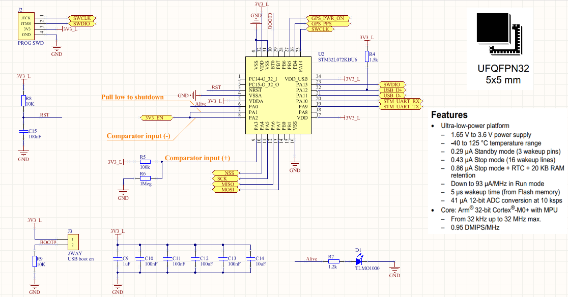
- The smart part is to use the same button to power down the thing. The EN pin also connects to the one input of the low power comparator of the MCU. The other input is connected to a reference voltage created by R5 and R6 on the MCU sheet, which outputs 3V. The divider created by D5-R14-R15 outputs a lower voltage: 1.8V. When you push the button, higher voltage comes from the battery and the comparator toggles. D5 is important because it does not allow high voltage on the 3.3V rail.
- The comparator triggers an interrupt and the MCU pulls down the EN pin of the 3.3v regulator. Of course, after you released the button.
- This way, I use the same button for hardware power-up and software power down.
Next, the MCU:

- J2 is the programming and debug connector: 4 holes 50 mils apart to accept a pin header. I will use the SWD interface.
- R8 and C15 keep the reset high.
- J3 and R9 change the boot option. If jumper J3 is fitted, the USB bootloader is enabled and a firmware update is possible.
- C9 to C14 are decoupling capacitors, as recommended by ST in the MCU datasheet.
- D1 lets you know that the circuit is operating.
- R5 and R6 create the reference voltage for the power-on and power-off circuit.
- R4 signals the USB host that a USB full speed device is connected.
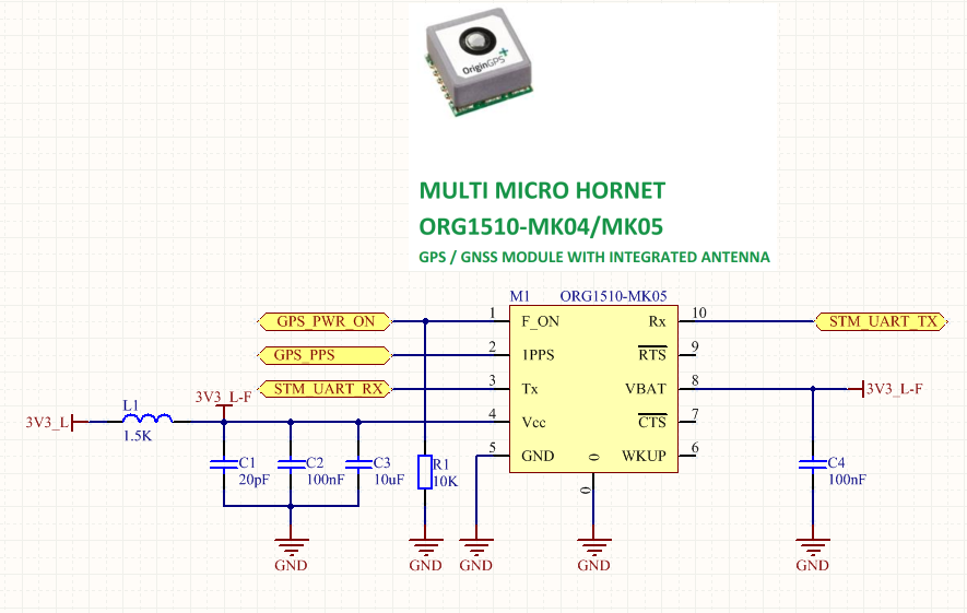
Moving on with the GPS module. Nothing spectacular here:

- L1 is a ferrite bead responsible for filtering conducted high frequency noise from the buck converter and the MCU.
- C1, C2 and C3, of increasing values decouple and filter even more the power line.
- There is no back-up battery at the Vbat pin, so a 100nF capacitor is required.
- R1 keeps the part in shut-down mode and it's enabled by the MCU.
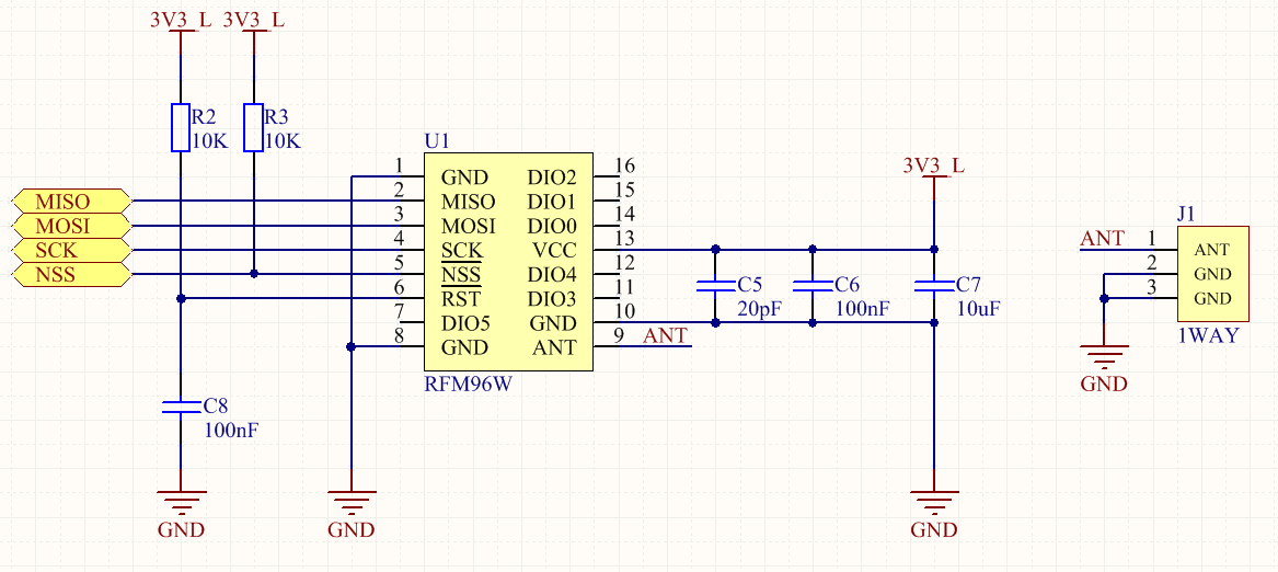
And the LoRa Transceiver:

The reset and the CS pin are kept high by R2+C8 and R3, respectively. The same combo of different value capacitors decouples the part.
On the left is the UFL connector.
Now let's proceed with the PCB layout. I am seriously considering a 4 layer board. I do not want to lose GPS fix when sending LoRa packets ...
Discussions
Become a Hackaday.io Member
Create an account to leave a comment. Already have an account? Log In.