 Kevin Neubauer
Why not start with the second hardest concept? I've never done RF design before, so this took quite a bit of reading. I read (mostly read, some skimmed) several white papers on RF PCB design before tackling this board. "Antenna Design and RF Layout Guidelines" by Cypress Semiconductor was approachable and well written.
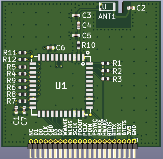
Four layer board stack-up:
- Top: Signal traces and components. Remaining space filled with ground pour.
- Layer 2: Ground plane
- Layer 3: 3v3 Power plane
- Bottom: Signal traces. Remaining space filled with ground pour.
Components:
- Realtek RTL8723BS module
- Unictron AA055A Wi-Fi & BT chip antenna
- 0402 Passives
Via Stitching/Fencing:
- In each corner and along board edges to arrest stray EMI from the power plane
- Fencing around RF keep-out zone & transmission line
- Between ground pours and ground plane to help maintain low inductance and provide short return loops
- All stitching and fencing was done between all GND pours and the internal GND plane
Other Notes:
- 50 Ohm impedance trace between RTL8723 antenna pin and chip antenna
- Calculation done using KiCad built in calculator for "coplanar wave guide with ground plane" and OSH Park 4 layer specs
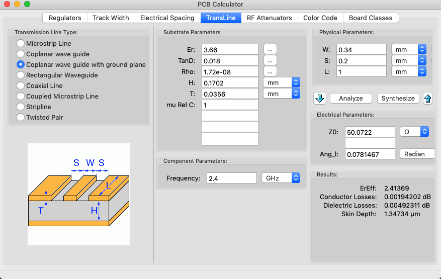
- Uninterrupted ground plane under RF transmission line
- Keep-out zone under chip antenna per Unictron datasheet guidance
- CNC cutout in keep-out zone per Unictron datasheet guidance
[Edit: The below calculation was wrong! I should have trusted my intuition and done more digging. :-) User @amorim317 helpfully pointed out that the below calculation does not factor in the substrate and its dielectric permittivity. Click here for new numbers.]
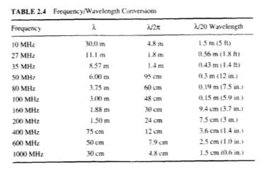
It seemed very difficult to find clear guidance on via fencing & stitching for RF layout. Most Internet sites refer to the frequency wavelength/20 guidance for determining spacing. However, they don't specify units and don't give examples! Frustrating to say the least, but it turns out it doesn't matter. It literally is as simple as finding your wavelength and dividing by 20... However, at the time I didn't think anything in RF design could be that simple, so I traced back to the source of this guidance. It originated from an IEEE Press white paper published in 1999 that was titled "EMC and the Printed Circuit Board. Design, Theory, and Layout Made Simple" by Mark Montrose. Section 2.9 of this paper gives the equation used along with a reference table of miscellaneous frequencies. Using this information, I was able to calculate the via stitching needed for 2.4 GHz. I used the middle of the band @ 2.45 GHz. The wavelength for 2.45 GHz is 122.45 mm. Take that divided by 20 and you get 6.1225 mm. My fence around my RF trace needed to have vias spaced 6 mm apart. After looking at 6 mm on my board and seeing how far apart it was compared with commercially produced 2.4 GHz PCBs, I decided to follow existing examples as closely as I could and use 0.75 mm stitching for both my RF fence and around the board edges and 2.5 mm stitching to join the ground pours with the ground plane. Extra vias on a small run board equals cheap insurance...
Discussions
Become a Hackaday.io Member
Create an account to leave a comment. Already have an account? Log In.
Thanks for the info! I'll check it out tomorrow.
Are you sure? yes | no
If you haven't already (and if it's not too late), check out Michael Ossmann's 5 simple rules for RF design:
https://www.youtube.com/watch?v=TnRn3Kn_aXg
His approach is pretty good, because he's basically a lay-person that developed a few rules to allow him and others to blindly follow to reliably get RF designs working.
Are you sure? yes | no