Kevin Neubauer
-
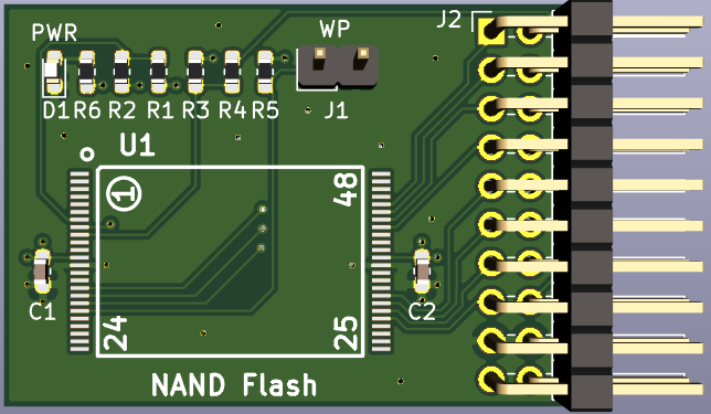
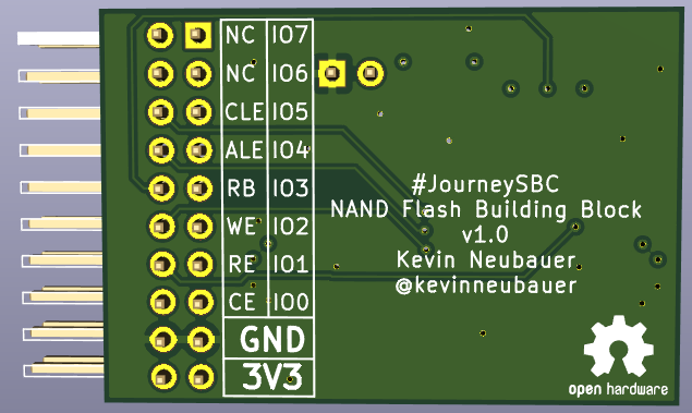
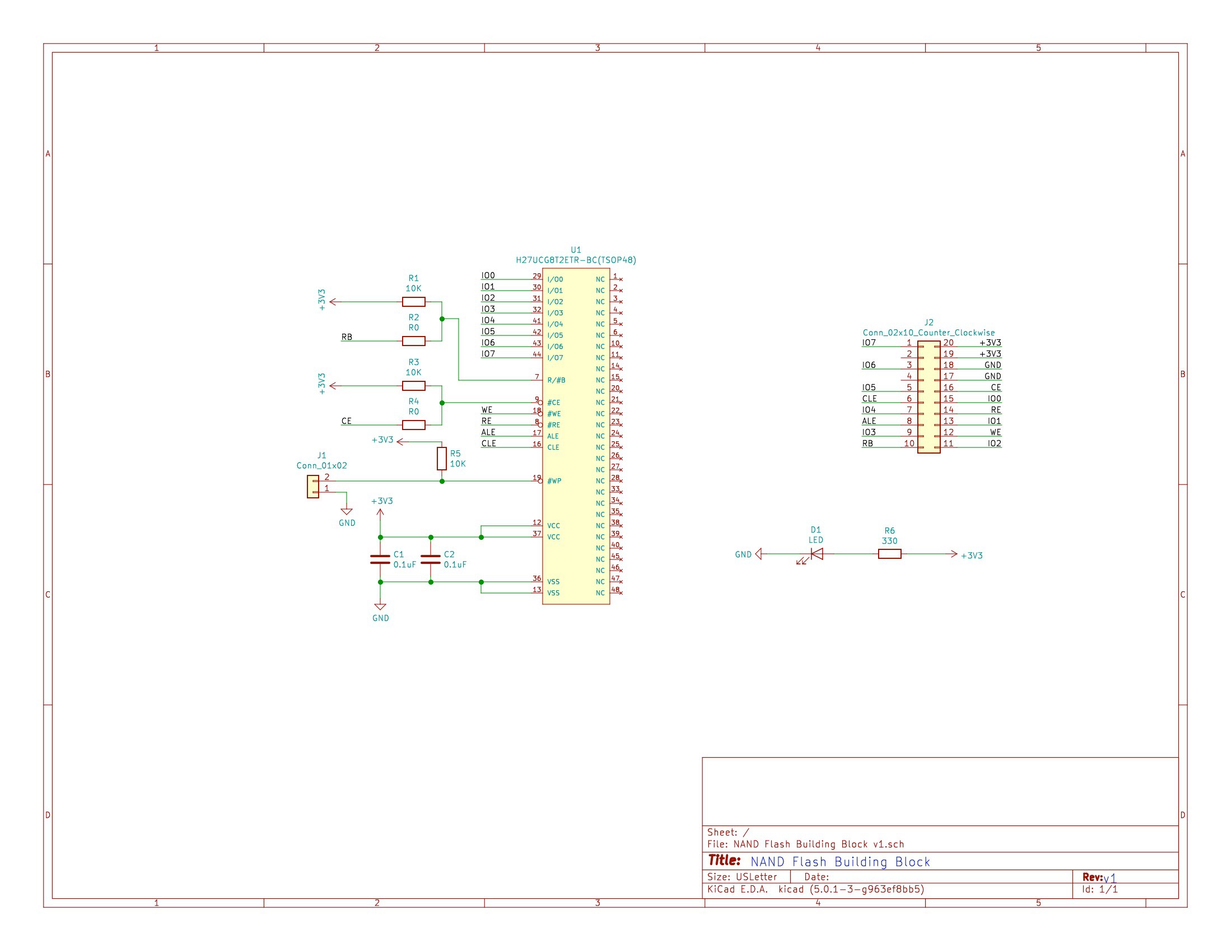
NAND Flash Building Block v1
11/25/2018 at 04:20 • 0 commentsI thought I would have no way of building a standalone peripheral PCB for testing out the NAND flash chip I wanted to use. I had no CPU & RAM mainboard yet and no other interface chips to work with the raw flash. Then it hit me. At the Hackaday Supercon this year, I took an FPGA workshop that was led by @Piotr Esden-Tempski. It was called "WTFPGA?" and I would highly recommend it if you want an into into FPGA technology. I looked around for existing OSHW designs to use (because why reinvent the wheel?) and lucked out. A company called Waveshare produces a (mostly) OSHW FPGA NAND interface board. They publish the schematic and pictures of the board, but I could not find board layout files. However, I am confident that with the schema and pictures, I could reproduce what I need for my flash chip.
After drawing up my own schematic, I set to work on the board layout. This board should allow me to test out my NAND, and after I'm done with it, I will be left with an added bonus. I will have a NAND module to play with for my new FPGA setup.
Four layer board stack-up:
- Top: Signal traces and components. Remaining space filled with ground pour.
- Layer 2: Ground plane
- Layer 3: 3v3 Power plane
- Bottom: Signal traces. Remaining space filled with ground pour.
Components:
- SK Hynix H27UCG8T2ETR-BC TSSOP48 NAND (8 GB)
- 0603 Passives
![]()
![]()
![]()
-
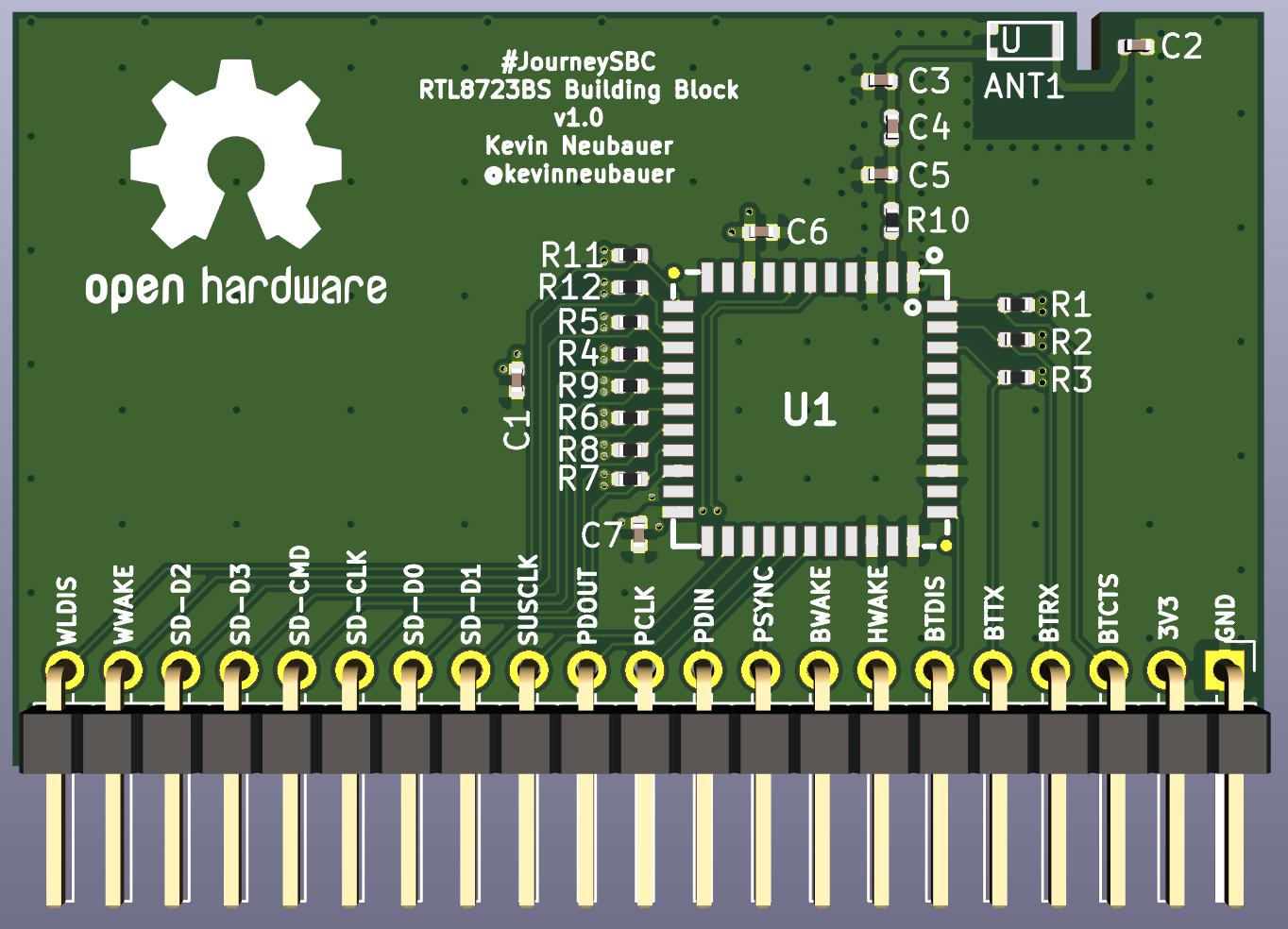
V1 Wi-Fi & BT Building Block PCB
11/16/2018 at 21:40 • 2 commentsSee here for the initial board stack up and features. Things haven't changed a lot between the initial draft and now. What has changed is via stitching/fencing, and the use of 2.54 mm header pins instead of the 1.00 mm header pins. I hate making a bigger board than I need for components, but it is what it is. 1.00 mm header pins aren't cheap or easy to find.
KiCad files posted to my GitHub. Link is on the main project page. If you like this design block and want to use it in any of your projects, you may want to wait until I get this assembled and tested.
![]()
-
RF & Via Stitching/Fencing Pt 2
11/16/2018 at 03:36 • 0 commentsBased on a tip from @amorim317, I found this article on via stitching that helped to explain why my original numbers were off. Turns out I was not factoring in my FR4 substrate into the equation. The original equation that I found only looked at the wavelength of the RF frequency in a vacuum, not its propagation through the FR4.
Based on the info in the above article, my via fence spacing in meters should be:
Where:
= Wavelength in a dielectric medium = Speed of light (299,792,458 meters/second) = Frequency (In this case 2,450,000,000 cycles/second) = Permittivity or dielectric constant of material (In this case 3.66) The frequency I'm concerned with is 2.45 GHz (2,450,000,000 cycles/sec). The dielectric constant of the 4 layer FR4 that OSH Park uses is 3.66 @ 1 GHz. If you look at the data sheet, it says 3.67 @ 2 GHz. I'm just going to use 3.66 because the difference is small, I'm lazy, and it's what I've already used to calculate my 50 Ohm transmission line.
Give the above, for my RF via fence we end up with a max distance of:
S(via) = 299,792,458 m/s / (20 * 2,450,000,000 * 1.913) = 0.003 meters * 1,000 = 3 millimeters
The article referenced above also recommends containing RF at board edges by using via stitching at wavelength/8 instead of wavelength/20. This means my edge via stitching should be separated by a max distance of:
S(via) = 299,792,458 m/s / (8 * 2,450,000,000 * 1.913) = 0.0079 meters * 1,000 = 7.9 millimeters
All of the above is very helpful in understanding the calculations involved in via stitching/fencing. If you're still reading, here's your reward: An easy to use calculator for TEM wavelength calculations! Take the result of the calculator divided by 20 to get RF trace via fencing max distance. Take it divided by 8 to get board edge via stitching max distance.
All of the above is great for validating your via spacing decisions. However, it doesn't factor any error or material differences or variability into the equation. I'm going to err on the side of extreme caution on my RF trace fence and use 1 mm spacing and cut down my board edge stitching to 5 mm.
-
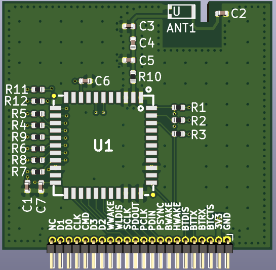
Always Print PCBs at 1:1 Scale Before Fabrication
11/15/2018 at 02:42 • 0 commentsI was just about to pull the trigger on ordering my Wi-Fi / BT board when I figured I should print it out on paper to double-check footprints. After printing at 1:1 scale, I realized the header pins were super small. I hadn't realized that I assigned a 1 mm pin footprint to my header part instead of a 2.54 mm (0.1")! I was probably distracted when I did it and equated 0.1" to 1 mm. I did look for a part source for the 1 mm header pins, but they were either expensive at around $7 for 50 pins or they had to ship from China. I decided to update the footprint.
Assigning the correct footprint, regenerating the nets, and then updating the nets in the PCB editor resulted in an immediate facepalm. I had to resize my board, rip up a bunch of traces, and then re-run them. The new board has a bunch of dead space on it, but it's needed to accommodate the larger header pin footprint...
Anyway, here it is. I'll likely order it tomorrow. After assembly, I'm going to see if it works and benchmark signal and throughput by using a Raspberry Pi.
![]()
-
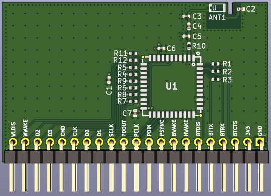
Wi-Fi & BT Perhipheral Board Progress
11/14/2018 at 05:25 • 2 commentsWhy not start with the second hardest concept? I've never done RF design before, so this took quite a bit of reading. I read (mostly read, some skimmed) several white papers on RF PCB design before tackling this board. "Antenna Design and RF Layout Guidelines" by Cypress Semiconductor was approachable and well written.
![]()
Four layer board stack-up:
- Top: Signal traces and components. Remaining space filled with ground pour.
- Layer 2: Ground plane
- Layer 3: 3v3 Power plane
- Bottom: Signal traces. Remaining space filled with ground pour.
Components:
- Realtek RTL8723BS module
- Unictron AA055A Wi-Fi & BT chip antenna
- 0402 Passives
Via Stitching/Fencing:
- In each corner and along board edges to arrest stray EMI from the power plane
- Fencing around RF keep-out zone & transmission line
- Between ground pours and ground plane to help maintain low inductance and provide short return loops
- All stitching and fencing was done between all GND pours and the internal GND plane
Other Notes:
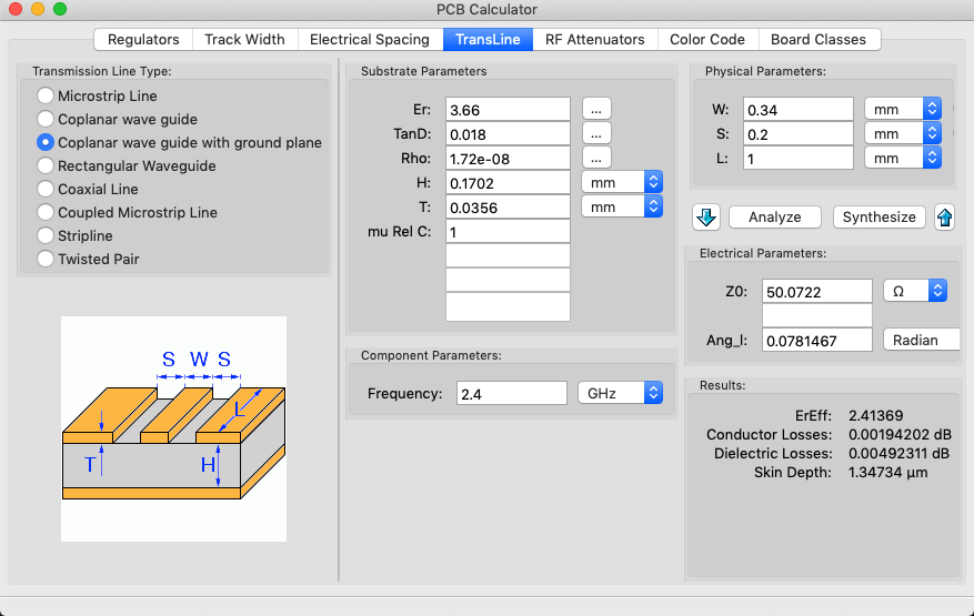
- 50 Ohm impedance trace between RTL8723 antenna pin and chip antenna
- Calculation done using KiCad built in calculator for "coplanar wave guide with ground plane" and OSH Park 4 layer specs
![]()
- Uninterrupted ground plane under RF transmission line
- Keep-out zone under chip antenna per Unictron datasheet guidance
- CNC cutout in keep-out zone per Unictron datasheet guidance
[Edit: The below calculation was wrong! I should have trusted my intuition and done more digging. :-) User @amorim317 helpfully pointed out that the below calculation does not factor in the substrate and its dielectric permittivity. Click here for new numbers.]
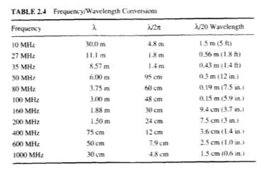
It seemed very difficult to find clear guidance on via fencing & stitching for RF layout. Most Internet sites refer to the frequency wavelength/20 guidance for determining spacing. However, they don't specify units and don't give examples! Frustrating to say the least, but it turns out it doesn't matter. It literally is as simple as finding your wavelength and dividing by 20... However, at the time I didn't think anything in RF design could be that simple, so I traced back to the source of this guidance. It originated from an IEEE Press white paper published in 1999 that was titled "EMC and the Printed Circuit Board. Design, Theory, and Layout Made Simple" by Mark Montrose. Section 2.9 of this paper gives the equation used along with a reference table of miscellaneous frequencies. Using this information, I was able to calculate the via stitching needed for 2.4 GHz. I used the middle of the band @ 2.45 GHz. The wavelength for 2.45 GHz is 122.45 mm. Take that divided by 20 and you get 6.1225 mm. My fence around my RF trace needed to have vias spaced 6 mm apart. After looking at 6 mm on my board and seeing how far apart it was compared with commercially produced 2.4 GHz PCBs, I decided to follow existing examples as closely as I could and use 0.75 mm stitching for both my RF fence and around the board edges and 2.5 mm stitching to join the ground pours with the ground plane. Extra vias on a small run board equals cheap insurance...
![]()
Journey SBC
My educational journey into the development of a single board computer.