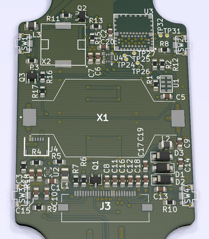
It is time to show the world my progress with this project. I uploaded it to github so you all can have a look and tell me what is wrong with it.
https://github.com/DasBasti/SchmartWatch_Hardware
Next to the KiCad project I also added PDF files of schematic and layout.
Please have a look at it and tell me your opinion before I put 1000$ into ordering a couple.
Here are a few infroations about the design.
The Board outline is designed to be fabricated as a flex PCB. There are a few stiffner areas where there should be a plastic plate supporting the flex board.
The watch is powered by a 3V coin cell that sits in the holder in the middle of the board.
From the cell the 3V are going to the RTC and the writst band brace. If the watch is closed around the wrist it closes the circuit and powers up the DCDC boost converter U2. This generates 3.3V for the whole system.
 Platinenmacher
Discussions
Become a Hackaday.io Member
Create an account to leave a comment. Already have an account? Log In.
before you do a flex run, why not order a cheap pcb run and test before?
Are you sure? yes | no
Hi dave,
I am thinking about this. The last FR4 run was on 0.4mm FR4 and worked quite well. You couldn't close the clasp though.
Are you sure? yes | no
@Basti if you'd like to send your design to support@oshpark.com, then our support engineers can take a look to see if there will be manufacturing issues. Thanks, Drew
Are you sure? yes | no
Will do thak. Thank you
Are you sure? yes | no
Hey, have you tested that piezo buzzer circuit?
I used a similar circuit recently, but with a resistor across it instead of an inductor, and it completely trashes my VCC line. Going to give it a shot with a flyback diode instead, I think.
Are you sure? yes | no
I will have a look at it again. Thank you.
Are you sure? yes | no
If possible, try to connect the pads of the connector to ground, just for stability. Not sure if the pads would peel off the flex otherwise. I've had someone on twitter tell me to watch out for unnecessary GND plane tongues. The R17 wire with via looks like it could be moved up a bit, to join the GND plane there.
Good luck with the board - are you trying out @oshpark for the flex pcbs?
Are you sure? yes | no
Yeah I was going to go for OSHpark, but I am not sure if I can handle the soldering of the components. So I am going for ~10 populated flex PCBs which will set me back aprox. 1000$. Therfore I want to have a lot more eyeballs looking over the design.
R17 does not go to GND plane, it goes down to the two right pins on J4, it crosses the trace going acorss from the battery to the RTC U1 on the right side of the board.
Are you sure? yes | no
meant to say join the ground planes. Put more space between the R17 via and the battery wire (the one where you put 4 vias around).
A lot of cash indeed o.O
https://www.dropbox.com/s/98l60ckhpvdzu15/Screenshot%202019-02-20%2015.53.00.png?dl=0
Are you sure? yes | no
OK got it. I also closed the plane on the bottom left at the push button.
Are you sure? yes | no