Another clock?
There is nothing particularly special about this clock, except perhaps that is is built from a 8042 microcontroller chip (henceforth MCU) salvaged from a very old PC. The most modern component is the integrated serial display which keeps the component count down.
Why did I embark on this project when I could have written this for a modern PIC or AVR MCU, which would be cheap enough and consume less power?
- I wanted to get back into the game and get up to speed with advances in MCU technology since I started decades ago. See my discourse in the next section.
- I have lots of chips of this era, pulled off PC motherboards. So I can take chances with them and not feel sad destroying something I bought.
- I wanted to do something substantial with these chips. There are a few pages on the Internet, for example DevSter and this video where people have got this MCU to work, and then were satisfied after getting LEDs to flash. The most complex one I saw ran a scrolling display.
- I wanted to push the envelope of these old chips and show that even with old technology you can achieve a low component count by design.
- I wanted to do something not run-of-the-mill. Anybody can wire up an Arduino to a serial display and write clock firmware in C. For this I needed to get low down with assembler and I already had most of the code from a previous project.
I believe constraints are good for learning to problem solve; they make you flex your mental muscles more.
Note that although I have designed a clock, the circuit can in fact be used for other purposes, it's all shaped by the firmware. You could make a metronome, a period timer or something else.
I will be putting logs of milestones in the log section and this details section will describe the results. So I may update the particulars if they change.
An entire section that used to be here has been moved to its own log to allow the narrative to flow better.
The 8042 family
The most widespread use of the 8042 chips was the keyboard controller in PCs, but only up to a certain time. After that the controller functions were taken over the 8051 family (possibly the most durable family of MCUs) or integrated in super BIOS chips. So to scavenge these chips look for very old PCs, say 486 and earlier.
The 8042 family of chips is similar to the 8048 family and has the same architecture inside, but was designed to be peripherals. There is also an External Access (EA) pin which is what allows us to put programs in external EPROM. The main differences are:
- Some instructions are deleted and some added. However these changes are generally not instructions you need. If you avoid those instructions, an 8048 assembler will work. Some like the ASXXXX series can be set to 8042 mode which catches any use of unavailable instructions.
- You cannot add external RAM if you need more than the 64 or 128 bytes internal RAM.
- In EA mode instead of multiplexing the data bus and the low byte of the address bus on the data lines, the low byte of the address is output on port 1. This means that you don't need an 8-bit latch to demux the data and address saving one interface chip. On the other hand, you lose direct access to port 1 and need a (different) 8-bit latch if you want to use this port. The bottom 3 bits of port 2 are always multiplexed and you would need a latch anyway if you wanted to use them. The top 5 bits are available as I/O pins as before.
- The T0 and T1 input pins are available too, but the I pin isn't. It is possible to trigger an interrupt by other more complicated means, but there isn't a testable I bit without using interrupts.
Now the members:
- 8041: 1kB mask ROM, 64B RAM, up to 6 MHz clock
- 8042: 2kB mask ROM, 128B RAM, up to 12.5 MHz clock
- 8741: EPROM version of 8041
- 8742: EPROM version of 8042
- 8242: An 8042 but with one of several off-the-shelf keyboard controller firmwares inside
I have not seen an 8241, presumably the keyboard firmware authors had no need to use a smaller version. There are supposed to be OTP versions of the 8741/8742. I have never seen those presumably because they ended up in the bin after use in a prototype.
Additional letters may indicate improved models, such as C for CMOS, which means lower current consumption. Get one of these if you need to reduce current consumption.
I suspect that the 8041/8741 chips are 8042/8742 chips that failed the clock speed and/or memory qualification and were packaged as slower/smaller versions. So it is possible that a particular 8041/8741 will be capable of 12.5 MHz if it was the additional memory that failed. I have a 8041 that works at 12 MHz. Here is some oral history from the people who created the 8048 family.
On the other hand I found on testing that some 8242s couldn't be clocked at 12 MHz. I think that these didn't need to be qualified to 12.5 MHz because they were driven at a lower rate on the motherboard.
So to be safe you should plan for 6 MHz. Particular ICs may clock faster. For example, all the 8742s I have do, probably because that's the advertised capability in the datasheet.
In this clock, the crystal is used as the timing reference. Due to a factor of three division in the MCU, to get an integral number of clock periods in a second, you will need a crystal frequency that is divisible by 3, e.g. 6 or 12 MHz because it will incur an error of about 1 second per day for every 12 parts per million that the integer divisor differs from the correct ratio. If you are using this board for other purposes where timing is not so critical, e.g. a metronome, then this condition doesn't have to be enforced.
Circuit design
I used this as an opportunity to learn to use Kicad. Fortunately version 5.0 was released recently and I could start with that.
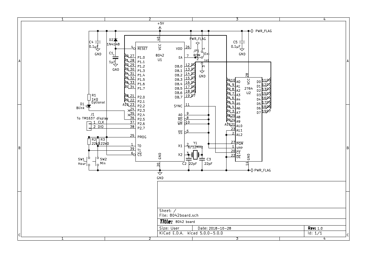
Here is the design:

There are several places on the Internet with cached copies of the UPI-41 or UPI-42 family datasheet, do a search with that term.
The 8048 uses the ALE output pin to multiplex the data and the low address bits. On the 8042 it's the same pin with the same function just relabelled SYNC. It nicely drives the /CE pin of the EPROM.
There are the usual noise bypass capacitors on the power lines as close as possible to the two ICs.
The reverse biased signal diode on the RESET line is to ensure the capacitor discharges quickly when the power goes down, so that it won't interfere with the next power up.
The blink LED can be omitted in production, saving 2 components, because it's just to verify that the circuit works.
The Kicad design files and the firmware will be put on Github when I have finished the project.
The serial line display
Originally I designed the circuit to drive 4 seven-segment LEDs multiplexed. This however requires a edge-sensitive latch to demux port 1 (e.g. 74LS374), a set of cathode drivers (e.g. 74LS244), some anode drive transistors, plus current limiting resistors. Then I saw that I could buy a 4 digit serial interface LED array using the TM1637 chip. As these modules are less than a couple of dollars from eBay, this was an easy decision to made, forsaking a bit of purity. If you want to directly drive multiplexed LEDs the option is there in the code.
Besides, I found that my old seven-segment displays were pathetically dim compared to modern LEDs (which is why you have LEDs displacing incandescent and even CFL bulbs for lighting), so I threw my displays out, well, put them in the e-waste collection.
I already had written firmware for a previous clock project involving a 8048, so I already had a leg up with the code.
Breadboarding the circuit
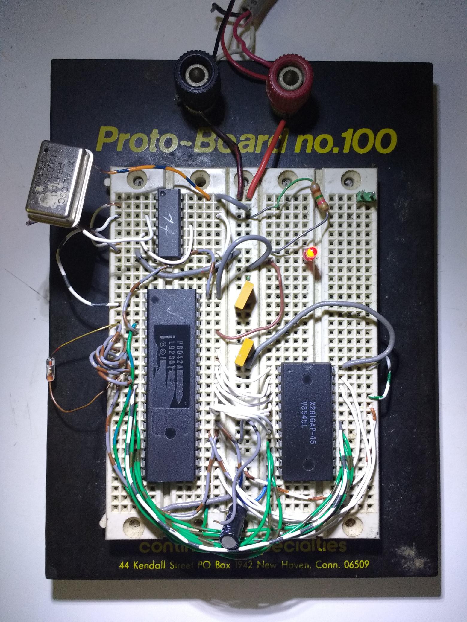
A picture of the breadboard:

Eagle eyed readers will notice deviations from the circuit.
The 2764 EPROM has been replaced by a 2816 EEPROM. In fact the 2764 (8kB) EPROM is already overkill since the program space of the MCU is 2 kB. However the 2764 is the first "hassle-free" EPROM after the confusion of the 2716/2516 and 2732/2532 EPROMs, explained here. You can in fact use any larger EPROM you have, you just to need to tie the unused address pins to ground. You could even use DIP switches on these lines to switch between different firmware at bootup. You can use an EEPROM like I did which speeds up testing, and if retained, allows faster upgrade of the firmware.
I used an active crystal frequency source because I didn't have any 12 MHz crystals on hand and have to order them, and also because I wanted to test the MCU at lower speeds, which accounts for the 74LS74 dual flip-flop at the top left wired up as a divide by 2 and 4 counter to generate 6 MHz and 3 MHz.
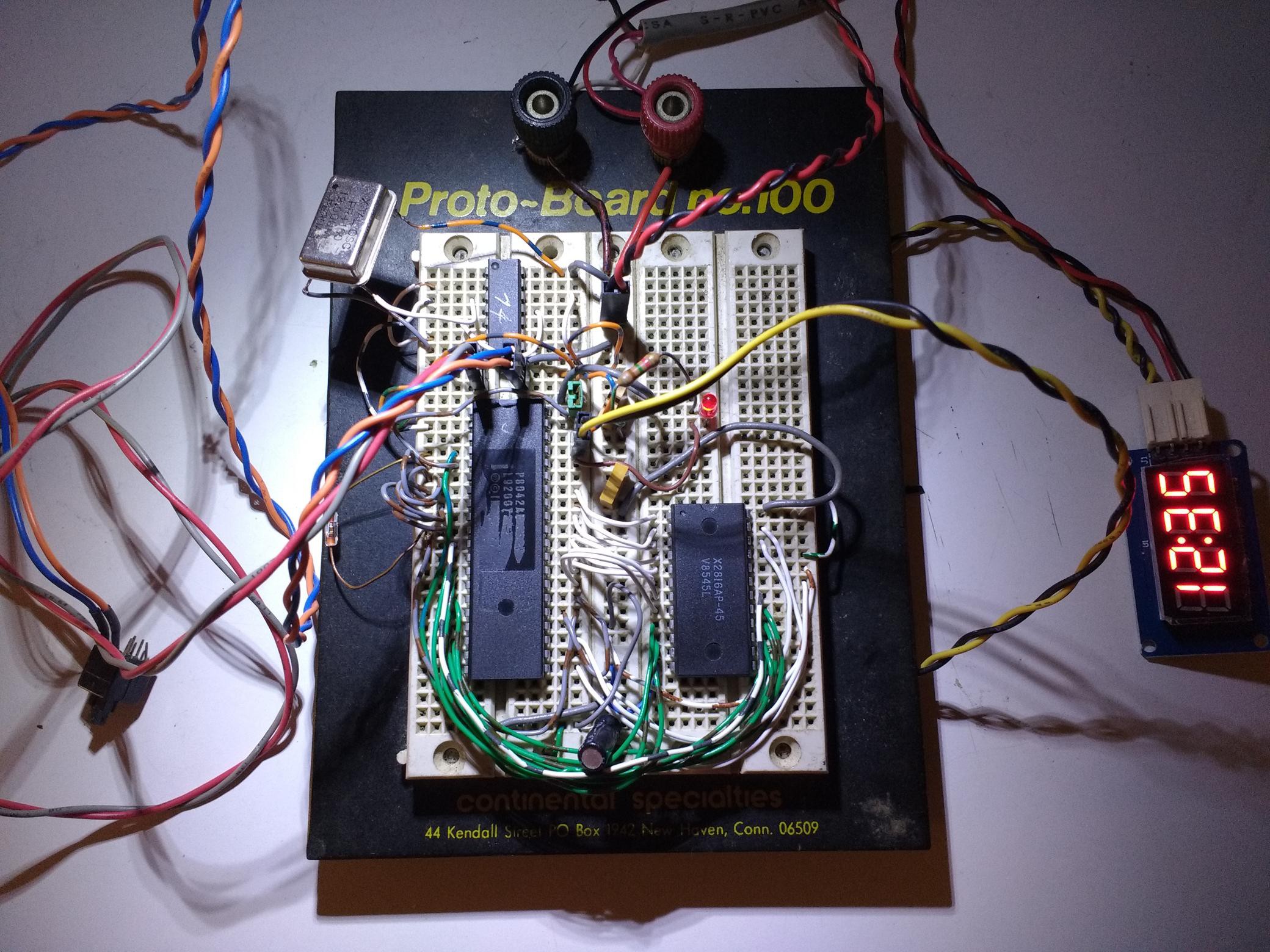
Time display working

The time setting buttons work as does the brightness control (pressing both buttons cycles the brightness level).
I will post pictures when I successfully build a production board but there won't be any major changes to these details from now on.
Production boards
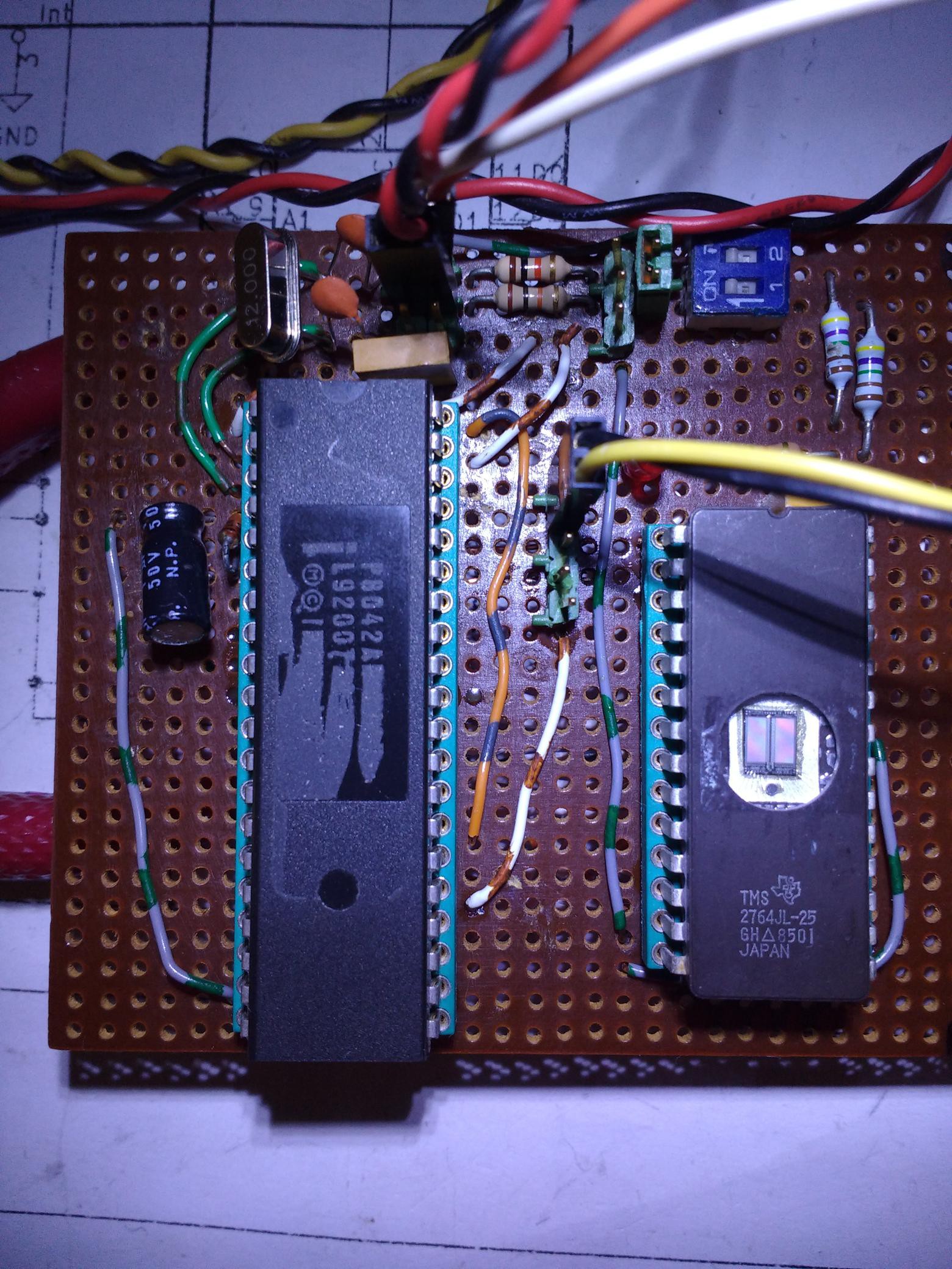
I think I will just make them on Veroboard despite the soldering effort. I'll leave the learning of the PCB design part of Kicad, and ordering over the Internet of boards, for a later project.
Here's a completed version:

One chip version
If I make a programmer for the 8741/8748 I can burn the program into the MCU, and dispense with the EPROM. Most EPROM programmers can't handle them due to the odd voltages required. I have plans for a design making use of an Arduino and an auxiliary power supply to do the programming, stay tuned for a future project.
Can't find a 8042 MCU?
This design can be adapted for the 8048 family. You just need to, as mentioned before, use a 74LS373 transparent latch to demux the data bus from the MCU for the address and data inputs to the EPROM.
Don't have an EPROM programmer (and eraser)?
Use an EEPROM which can be rewritten with a simpler circuit not requiring more than 5V supplies. Designs for EEPROM programmers can be found easily.
 Ken Yap