 xBeau
xBeauThe "outputs" of what looks like the production version of the PCB's for both badge and expansion were posted to the official badge project, the zips contain a sub-folder with gerber files.
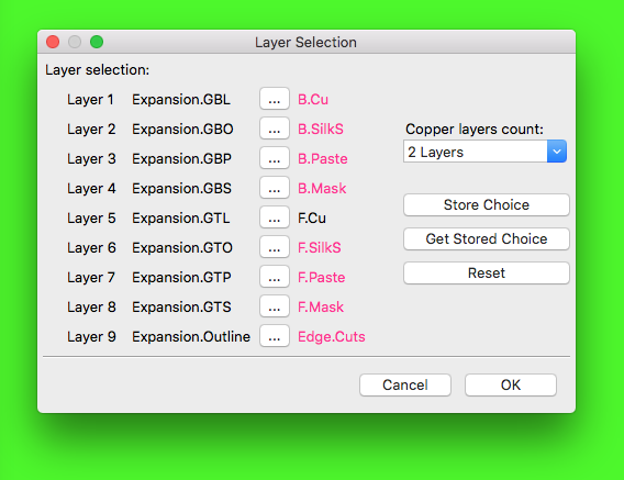
In the process of converting the gerber files into a KiCad board file, you will get the following layers doing "Open Gerber Files...". Note that these leaves out a number of layers that use other file extensions naming conventions. The "Outline file was manually imported by selecting the "*.*" file type option.
- *.GBL (Bottom Layer / B.Cu)
- *.GBO (Bottom Overlay / B.SilkS)
- *.GBP (Bottom Paste / B.Paste)
- *.GBS (Bottom Solder Resist / B.Mask)
- *.GTL (Top Layer / F.Cu)
- *.GTO (Top Overlay / F.SilkS)
- *.GTP (Top Paste / F.Paste)
- *.GTS (Top Solder Resist / F.Mask)
- *.Outline (Border / Edge.Cuts)
The mapping to KiCad layer names is shown after the Gerber convention. This comes in hand when using the Export to Pcbnew from Gerber viewer.
Also note that for whatever reason when I converted the *.Outline to Edge.Cuts, I got a duplicate outline of one on top of the other, which just caused the laser cutter to cut the same path twice.
Discussions
Become a Hackaday.io Member
Create an account to leave a comment. Already have an account? Log In.