-
If you don't have any Dollars ?
09/27/2019 at 20:28 • 3 commentsIf you don't have dollars (Sorry I mean diodes), and you don't want two different current directions in your A and B inputs... What would be an easy ALU circuit ?
![]()
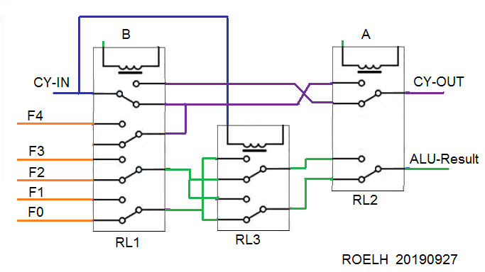
The above circuit will do all possible logic functions, and will also ADD.
The controls are a lot like that of the 4-bit TTL ALU, as described in ITS FIRST Log. It also operates in much the same way.
If F4 has no power, then none of the RL3 relays will attract. In this case, the four inputs F0 - F3 determine which of the 16 possible logic functions is executed. Of course, the CY-IN of the first circuit must also not be activated.
For addition, F4 must be powered and the XOR must be selected as operation (F2 and F1 powered). Note that there is no built-up of carry delays.
If you also want a shift-right for your one-byte ALU, then add two 4-pole relays to select the normal ALU result or a shifted version of it.
Note that the upper contact of RL1 has been mirrored in the drawing, to make it easier for you to follow the current flow. Also note that the ground connection of the relays is not shown.
-
10 functions now, for a few diodes more...
11/09/2018 at 15:51 • 1 comment![]()
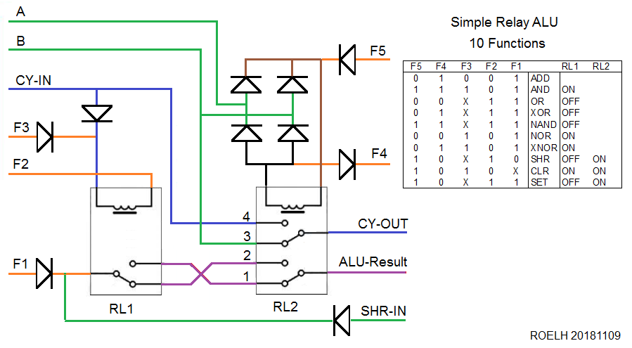
Yesterday I entered this project on Hackaday. But thinking never stops. I tried to find a use for the fourth contact on my 2 DPDT relays, but ended up with a similar 3 SPDT solution (good news for Yann), with 5 more functions.
![]()
The key is the bridge rectifier for the relay RL2. Two new control signals F4 and F5 can now control RL2, together with the two inputs:
With F4=1 and F5=0, RL2 attracts if A and B are different, just as before.
Now make F4=0. RL2 now always has ground, so will attract if either A or B is high, providing the OR function.
Now consider making F4=1 again, and make F5=1. RL2 now always has 12 volts, so it will attract if either A or B is low, providing a NAND function.
RL1 can still be controlled with the F2 and F3 signals. It controls the polarity of the output signal, so when RL1 is attracted it will transform XOR to XNOR, NAND to AND and OR to NOR.
If we now make F5=1 and F4=0, RL2 will always be attracted. This gives an always-zero (CLR) at the output when RL1 is OFF, and always-one (SET) if RL1 is ON.
In this final situation, the voltage for the always-on comes from control F1. If we now make F1 low, this voltage is controlled by the SHR-IN input, that is connected to input A of the next bit. So it will give us the Shift-Right function (SHR). A 74181 can't do that ! Note that a Shift-left is already available because it is the same as adding a number to itself.
Only SUB and PassThrough functions are missing. A PassThrough function can be made by clearing the other operand and doing ADD or OR. Subtract might be done by doing a negate function first (XNOR with zero), or inverting the A or B signal in a previous circuit (as in the RISC Relay CPU).
-
Description of the logic functions
11/08/2018 at 13:49 • 0 commentsFor the logic functions, a Carry-out is generated just as for the ADD function. But the carry input is ignored because the relay RL1 is forced to an active or non-active state by inputs F2 and F3, so it is no problem that there might be a signal present on the Carry-out of the previous stage.
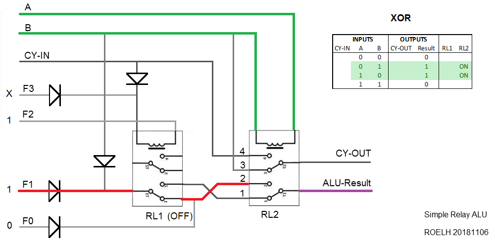
The simplest function to explain here is XOR:
![]()
The control input F2 must be logic 1 (or floating). This ensures that RL1 is always off. If A differs from B, relay RL2 will connect the ALU-Result to the logic 1 provided by control F1. Otherwise, the result is not connected (meaning logic 0). The XOR function will be selected if either F0 or F1, or both are "1".
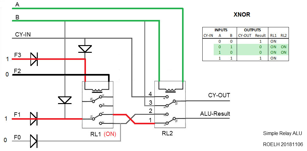
The next one is the XNOR function:
![]()
By making control input F3 active and F2 ground, relay RL1 will be always ON. Now, the ALU-result will be logic 1 when both inputs are equal, providing the XNOR function.
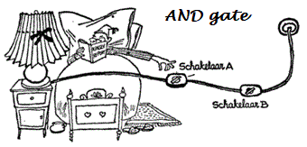
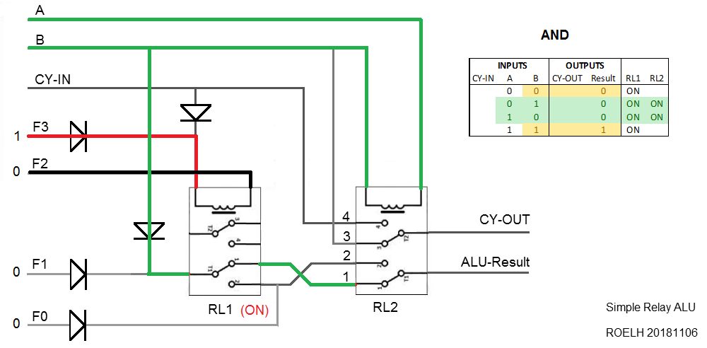
Now to describe the AND function:
![]()
![]()
The only difference with the previous (XNOR) situation is, that control F1 is now 0. The result is, that the signal on input B now flow through a diode to connection 1 of relay RL2. The ALU result will only be one if RL2 is OFF (so both inputs equal) and input B is 1. So, it is only one if both A and B are 1.
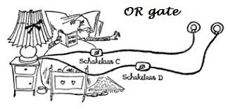
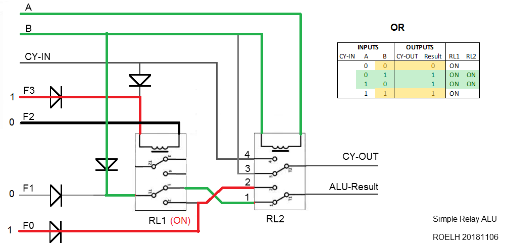
The last function is OR:
![]()
![]()
The only difference with AND is, that control F0 is now active. This causes an active ALU-result when A and B are different. When A and B are the same, the result is 1 if B is 1 (as in AND). Together, this delivers the OR function.
( The AND-gate, OR-gate pictures were taken from R. Lohberg and Th. Lutz: Hoe werkt een computer?, Kluwer (Netherlands) 1968. )
-
Description of the ADD function
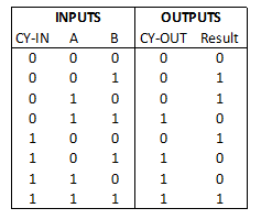
11/08/2018 at 13:20 • 0 commentsAs a reminder, the ADD function has to produce two output signals according to the following table:
![]()
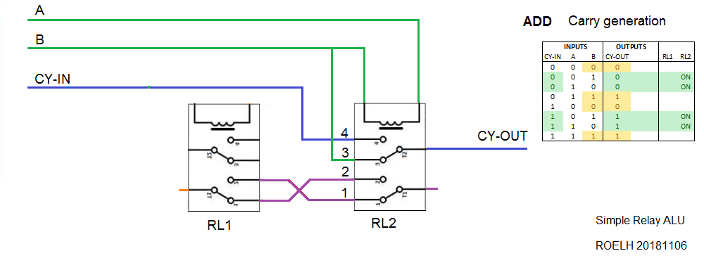
The next diagram illustrates how the CY_OUT signal is generated:
![]()
Only relay RL2 is involved for CY-OUT generation. RL2 is activated when the signals A and B are different (indicated in green in the function table).
When RL2 is activated, the Carry-output is the same as the Carry-input.
When RL2 is not activated, the Carry-output is the same as input B (indicated in yellow in the function table). It could also be connected to the A input, since A and B are equal when RL2 is not activated.
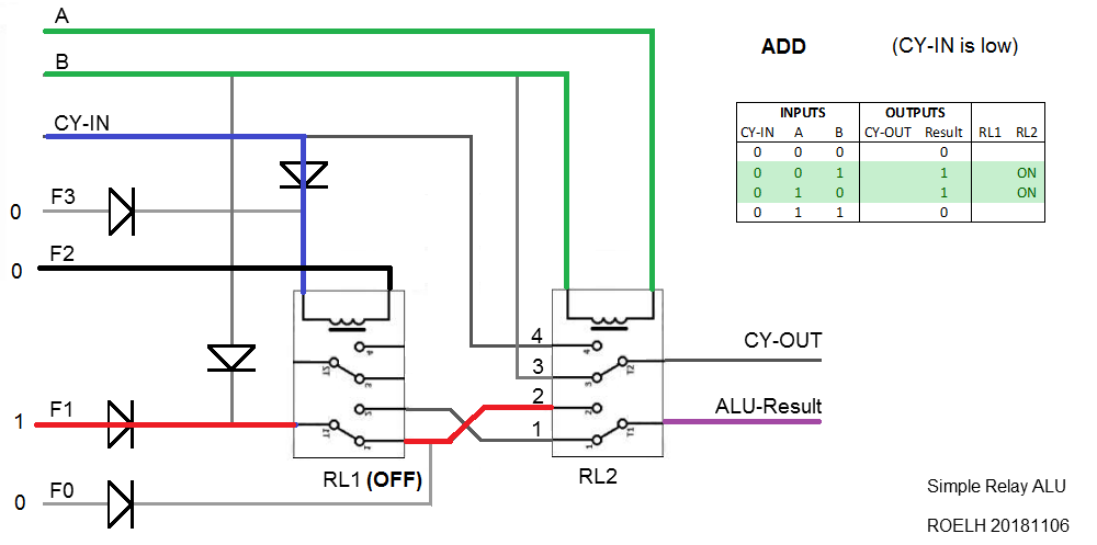
For the result output, I use two pictures, one for [Carry-in = 0] and one for [Carry-in = 1].
![]()
Relay RL1 is connected to the Carry-in signal, so it is not attracted when Carry-in is 0. Input F1 provides logic 1 to connection 2 of RL2. Relay RL2 attracts when A differs from B, so the result is (A xor B) according to the table.
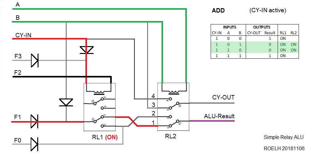
![]()
When the Carry-in is 1, RL1 is always attracted. This time, input F1 provides logic 1 to connection 1 of RL2. So the output is only logic 1 when both inputs A and B are equal.
Simple Relay ALU
Only 2 relays and a few diodes, but 10 functions including ADD and Shift Right. Simplest relay ALU ever designed ?