Keith
Keith-
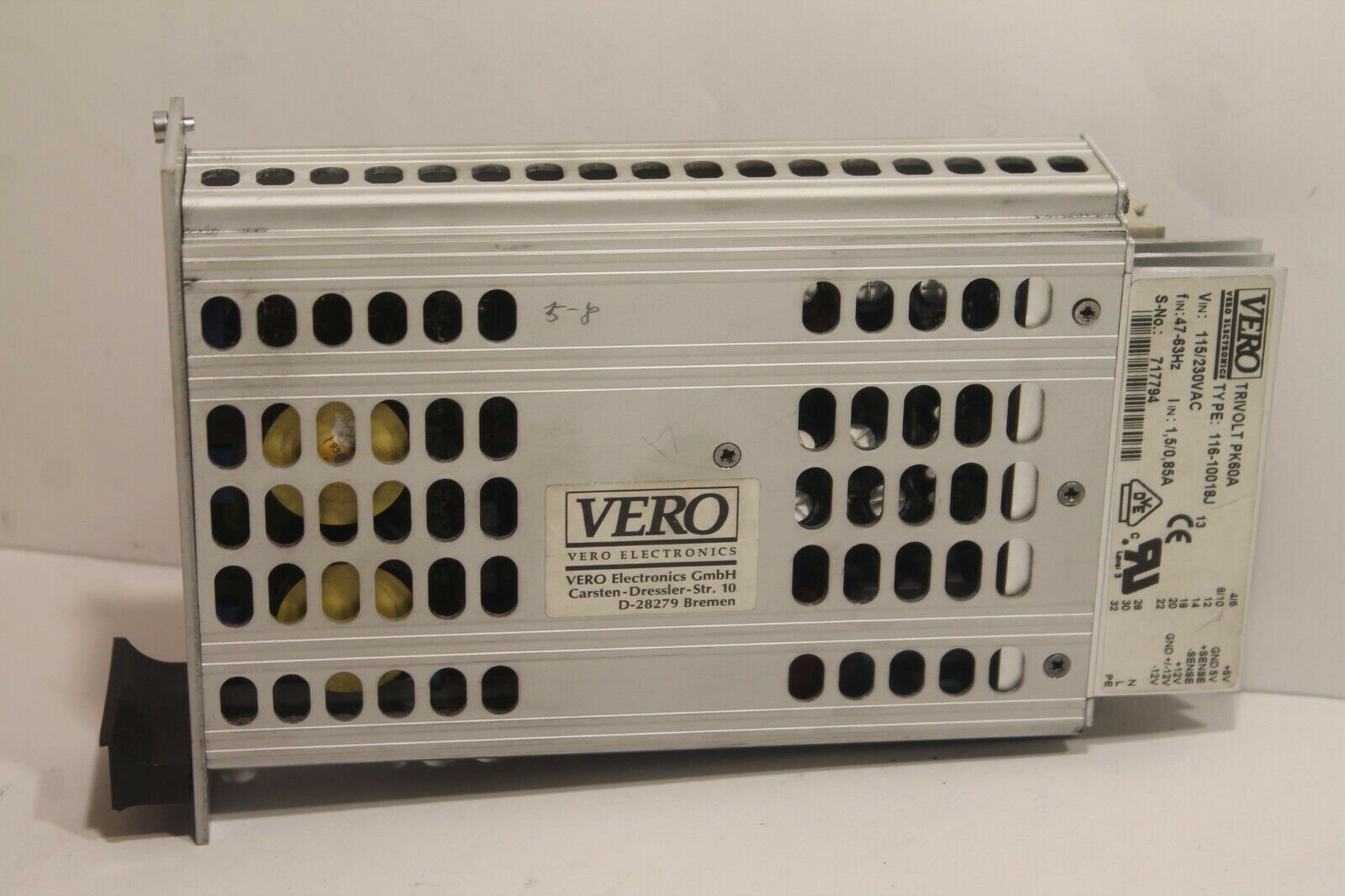
Power supply
01/21/2023 at 13:58 • 0 commentsI suspect the power supply in the enclosure might be flaky, so I am looking to try a different one.
I have a rack mounting supply, from Vero Electronics, PK60A type 116-10018J. Rated 5V 6A, and +/-12V at 1A.
![]()
Needs a chunky DIN connector which I don't think I have. The mating connector will also need wiring terminated with Faston connectors, which I can obtain.
2023-01-24
I have a small board I use for powering single STEbus masters from a wall-mounted 5V PSU. It connects the 0V and 5V from a 2.1mm power connector to the 0V and 5V of a female DIN-41612 connector. It has a 5V to +/- 12V DCDC converter, to power the RS232 buffers.
The first converter died due to the excess drain of a chip inserted the wrong way round.
Today I replaced it with a 2W version. https://www.farnell.com/datasheets/2787714.pdf
Small DCDC converters are usually poorly regulated. This one was +/- 18V unloaded. The MC1488 buffer chip is +/- 15V max. Fortunately, the rails drop to about +/-12.5 volts when loaded by this chip.
This worked but did not cure the disk failure problem.
-
Floppy drives
01/16/2023 at 00:51 • 0 comments2023-01-15
The rack-mounted drive is an NEC FD1035, taking 2W on each of two power rails.
Therefore 12V is 2/12 = 0.167 amps, and 5V is 2/5 = 0.4 amps.
The drive of unknown provenance is a TEAC FD235HF which requires only 5V at 0.8 amps peak, i.e. 4 W total peak power.
I don't know why they are behaving differently, other than maybe one is dead. The FD1035 is single density. So I may simply buy a new FDD that is guaranteed working.
2023-01-16
Made a new 34-way ribbon cable, just to make sure the cable is not the problem.
The FDD that didn't respond did not even light its LED so I guessed it was not seeing its drive select signal. I looked for a link suggesting drive selection. There are no jumpers but there was a surface-mount 0R resistor in a position marked DS1 which it shared with one marked DS0. Moved the resistor to DS0 and the drive responds in the same way as the first FDD.
Two boards, two drives, four combinations, one disk. I think the problem is the disk. The CP/M manual for this board says the sectors are interleaved in the order 1, 6, 2, 7, 3, 8, 4, 9, 5 but it is failing to read sector 1 so the interleaving is not the issue.
2023-01-19
New FDD arrived today. Familiar problem, needed opening up and a solder-blob link changing to the DS0 position. Familiar result, sectors not reading. This is with the FDD and processor board driven by two different power supplies. Not ideal.
Changed to Steve's board, powered by same crate as the FDD. I did not get an instant sector fail, but did get an error eventually on track 2, which implies track 1 had been read successfully.
Wondering if the disk is slightly off centre, I eject then reinsert it. This seems to help. After quite a few "Retry? y" cycles, it appears to boot.
Press RETURN

Arcom ATLAS
Serial console running at 9600 baud

Insert system disk in drive A: and press RETURN

CP/M V3.0 Loader
Copyright (C) 1982, Digital Research

BIOS error on A: Track-002, Side-0, Sector-006, Read, Not ready.
Retry (Y/N)? y
BIOS error on A: Track-002, Side-0, Sector-006, Read, Not ready.
Retry (Y/N)? y
BIOS error on A: Track-002, Side-0, Sector-006, Read, Not ready.
Retry (Y/N)? y
BIOS error on A: Track-002, Side-0, Sector-006, Read, Not ready.
Retry (Y/N)? y
BIOS error on A: Track-002, Side-0, Sector-006, Read, Not ready.
Retry (Y/N)? y
 51K TPA

BIOS error on A: Track-003, Side-0, Sector-001, Read, Not ready.
Retry (Y/N)? y
BIOS error on A: Track-003, Side-0, Sector-001, Read, Not ready.
Retry (Y/N)? y
Arcom ATLAS CP/M 3 BIOS V1.5
Copyright (C) 1984, Arcom Control Systems Ltd.

BIOS Error on A: T-00001, S-00000, Read, Not ready, Retry (Y/N)? y
BIOS Error on A: T-00001, S-00000, Read, Not ready, Retry (Y/N)? y
BIOS Error on A: T-00002, S-00000, Read, Not ready, Retry (Y/N)? y
BIOS Error on A: T-00002, S-00000, Read, Not ready, Retry (Y/N)? y
BIOS Error on A: T-00002, S-00000, Read, Not ready, Retry (Y/N)? y
BIOS Error on A: T-00001, S-00000, Read, Not ready, Retry (Y/N)? y
BIOS Error on A: T-00001, S-00000, Read, Not ready, Retry (Y/N)? y
BIOS Error on A: T-00001, S-00000, Read, Not ready, Retry (Y/N)? yA>
A>dir
A: CPM3     SYS : BDOS3    SPR : BNKBDOS3 SPR : RESBDOS3 SPR : BIOS3    SPR
A: BIOSKRNL ASM : BNKBIOS3 SPR : BOOT     ASM : BOOTB    REL : BOOTN    REL
A: CHARIO   ASM : CHARIO   REL : COPYSYS  ASM : CPMLDR   REL : DRVTBL   ASM
A: FDPH     ASM : FLOPPY   REL : GENCPM   DAT : HELP     HLP : MEMORY   REL
A: SCB      ASM : SCB      REL : TIME     ASM : TIMES    ASM
SYSTEM FILE(S) EXIST
A>
On the good side, it looks like the sectors are valid and it manages to run the DIR command from the serial line okay.
This success is short-lived. An attempt to PIP BIOSKRNL.ASM creates more errors.
The hardware manual says:
"If your drives are not working reliably (a good test is to format a disc) the most likely cause is not maladjustment but electrical (or more probably magnetic) interference. A typical symptom is an increasing error rate on the inner (higher numbered) tracks when trying to format discs. Check this by moving the drives and the SCPUA board away from all possible sources of interference, including VDTs, monitors, switch-mode power supplies and mains cables. A noisy power supply to the SCPUA will also increase the error rate."
I shall investigate the PSU. After decades, the smoothing caps may have dried out. The meter reads 5V and 12V correctly.
2023-01-21
The original system in the case was a 68020 running OS9/68K from a SCSI disk, and that also failed to boot. Perhaps that was also a power supply problem.
I removed the FDD power lead off the crate and wired it to the same power rail as the board. I then plugged it into a 5V-only FDD. The system power was a modern 5V 3A wall wart, which is more than the 2A expected load. Same failures as before, so I am beginning to think the power supply is not to blame.
Maybe the disk magnetisation signal is borderline?
-
My board
11/26/2022 at 02:25 • 0 comments2022-11-26
Fitted copies of PAL chips from Steve's board.
Assembled code reverse engineered from Steve's board, and modified for an FDC with a non-inverted data bus.Missing chips:
IC 9 = 74LS123 replaced with 74HC123.
IC 13 = 74LS273 which I don't have but could borrow from another board.
IC 16 = MC1488 is an RS232 buffer, I have some spare.
IC 17 = MC1489 is an RS232 buffer, I have some spare.2022-11-27
Wondering how to tap the TTL-level serial signals to use an FTDI USB cable, I realised the parallel keyboard port has 16 pins and is fairly redundant because parallel keyboards are obsolete.
I had a look at the pinout and looked for a way to plug in the USB cables with the least effort.
By very good fortune there seems to be a way to route both serial channels to this header, with only the USB VCC (wire 3) needing to be disconnected and the USB !CTS (wire 2) moving to position 3:
USB
cable
fn (pin)Serial
Channel
A (pin)PL3 Serial
Channel
B (pin)USB
cable
fn (pin)!RTS (6) !CTS (18) kb d3 1 2 kb d4 !CTS (22) !RTS (6) RXD (5) TXD (15) kb d0 3 4 kb d2 TXD (25) RXD (5) TXD (4) RXD (13) kb d1 5 6 kb d7 RXD (27) TXD (4) !CTS (2 := 3) !RTS (17) kb d6 7 8 kb d5 !RTS (23) !CTS (2 := 3) VCC (3) := nc dnc GND 9 10 VCC dnc VCC (3) := nc GND (1) GND 11 12 GND GND GND (1) DTRB 13 14 DCDB DCDA 15 16 DTRA This requires the RS232 buffers to be removed and four wires per channel to be routed to the keyboard data lines.
The keyboard data port is an input only, so the keyboard buffer chip IC30 does not need to be removed.
2022-11-28
I modified a USB cable as above, and added four wires from the SCC to the new cable header, and applied 5V power.
Nothing on the terminal. Logic probe showed the clock circuit working but CPU clock pin stuck high. Ditto the clock of the DRAM controller. Maybe a PCB track break that could be fixed with a wire?I got Steve's board out to compare continuity. At this point I noticed the three 40-pin chips were the opposite way round! Close inspection of the pips on the PCB legend showed that these chips really are meant to have the polarity pips the opposite way round to all the other chips on the board.
Being powered up the wrong way round did not cause any to emit smoke, or get very hot, so I rotated them 180 degrees and hoped for the best. I was disappointed, no text on the terminal.
With all comms failures, experience has shown that the first question is to ask "have you got TX and RX wires the wrong way round?". This is an easy experiment so I swapped them over.
Success! I got a sign-on screen like this:
Press RETURN

Arcom ATLAS
Serial console running at 9600 baud

Insert system disk in drive A: and press RETURN

Unknown disk format
Insert system disk in drive A: and press RETURN
This proves the board is largely healthy and is working as expected for a board with no disk drive attached.I have a drive and blank disks, but no system disk. So I can't try reading a known-good formatted disk.
All I can do for now is to go through the FDC setup procedure to check the critical timings are correct.
I have also swapped CTS/RTS over.
2023-01-15
Unable to find 34-way FDD cables! I must have thrown them all out as very obsolete technology. Being impatient, I hacked down a 40-way cable.
Connected my board and my own FDD with the sawn-off cable. Placed board in case and switched on. Inserted disk from Steve, and got nothing. Puzzling.
I moved the board to my test rig, where it worked before, and it signed on. I then switched it off, attached the rack-mounted disk drive, then switched the board then the drive power on.
Press RETURN

Arcom ATLAS
Serial console running at 9600 baud

Insert system disk in drive A: and press RETURN

Error reading system disk:
Track-000, Side-0, Sector-001, Record not found, Retry (Y/N)
This is good in that it got as far as reading the floppy drive. The drive is pretty old, and the eject button is very stiff.
I tried a different drive, which did not have a stiff eject button. I got this:
Press RETURN

Arcom ATLAS
Serial console running at 9600 baud

Insert system disk in drive A: and press RETURN

Unknown disk format
Insert system disk in drive A: and press RETURN
Not so good.
This is now the same behaviour as Steve's board.
-
Steve's board
11/13/2022 at 13:42 • 0 commentsSteve reported some problems with his board. The reset generator (IC9, SN74LS123, a dual monostable) was holding the reset lines to the FDD controller and Z80 low. It should reset the FDD controller first, then the Z80. Not having a spare to hand he replaced the IC with a header containing 2 RC circuits, and the Z80 now starts reliably, so the EPROM content is probably good.
I suspect the 4µ7 electrolytic capacitor C10, controlling the reset pulse, will have dried out and needs replacing.
The FDD controller does not appear to be working correctly. Whe put it into 'test' mode as described in appendix E of the manual, the VCO clock was not running.
If the FDD controller is dead it may be difficult to replace - Cricklewood Electronics stock the WD2793 for £78 and the WD2797 for £15 but not the WD1791. The WD2797 is not compatible because pin 25 is the Side Select Output instead of Enable Mini Floppy input. The SCPUA board has this pin wired to the 5/8 inch drive size select, so there would be two outputs driving the same wire.
The WD2791 FDC chip is still obtainable (£30 from ebay).
The WD2793 is similar but with a true data bus ( £28 from ebay) so the latter could be used with trivial mods to the firmware. I have added conditional assembly to the firmware so it can assemble for either the 2791 or 2793. As a bonus, the disk i/o will run slightly faster, because the disk data does not have to be inverted by software.
The 2793 is used in the Atari 800 series machines, and is available from Best Electronics for $16.
FDC chip supply was a headache even in the 1980s. The WDx79x chips came in four variations, and if one of them became unobtainable then you were stuck. For this reason, Arcom's FDC board was designed to use any variant, by having the chip data passed through inverting or non-inverting buffers, and having the functions that differed controlled by TTL chips instead.
2022-11-18
Steve's SCPUA arrived. Known-dead LS123 removed, destroyed, and replaced with my (presumably working) LS123 from my board.
I flipped it over to look at the underside, instantly spotted two unsoldered pins! Pins 8 and 9 of IC11, a 74LS93, drive the master clocks CLK2 (2 MHz to the FDC) and CLK4 (4 MHz for the CPU and DRAM controller). Joints now soldered.
It has no serial number. The test department only assign serial numbers to boards that pass testing. Maybe it missed the test procedure?
2022-11-20
5V applied to Steve's board. A quick probe of important pins:
IC10 (CPU)
6 CLK 4 MHz
26 /RESET 5V DC
19 /MREQ 1.2 MHz
21 /RD 0.9319 MHz
22 /WR 0.1794 MHz
27 /M1 0.4 MHzIC12 (TMS4500)
1 CLK 8MHzIC18 (FDC)
24 CLK 2 MHz
19 /MR 5.04 V DC
3 /CS 4.723V 0.16 MHzIC15 (SCC)
20 CLK 4 MHzIC9 (74LS123 reset circuit)
2 B 2.562 V DC
4 /Q1 5.046 V DCIC8 (ROM)
20 /CS 0.8 MHz
22 /OE 0.931 MHzLooks good so far. Healthy clocks, out of reset, accessing the ROM and FDC chip. Next step is to see if the sign-on message appears. Steve said it already got that far, but failed to recognise a CP/M disk from the 1980s. Following the instructions in appendix E of the SCPUA manual (connect pin 22 of the disk controller to pin 20 (ground)), he found that the VCO (as measured on pin 16) was not working. He has some doubts about the instructions in appendix E, as the value measured for step (3) was quite a bit different from the target value of 500ns. I shall make a note of the observed settings before making adjustments, just in case the instructions are wrong.
I need a break to find my collection of FTDI USB to Serial interfacing cables and dongles.
I read the three PAL chips and disassembled the logic, and put the pin names in. This clarified a lot of the workings. They differ a lot from my two logic chips, which don't seem to make great sense, so I suspect they were just prototype or junk.
I shall copy Steve's PAL logic to some new GAL 16V8 chips for my board, and create a boot ROM modified for my FDC chip. Tandem debugging may help - what they do the same is probably right, and if they differ then one of them must be wrong.
2022-11-23
I soldered on a ground wire (for the scope) and a switch for joining the FDC pin 22 to ground. Tweaking the trimmer devices adjusted the signals on pins 29, 31 and 16 as expected. I forgot to measure what they were to start with, but left them in state expected. The master clock is 2 MHz. It is not possible to adjust the VCO to 250 kHz ±5 kHz by eye, I shall fine-tune it by measuring the frequency with a multimeter.
That done, it will be ready to try with a floppy disk drive.
2023-01-13
Timing adjusted, looks correct. Measured on accurate meters.
Made an Arcom RS232 10-pin header to IBM PC 9-way D-type adapter.2023-01-15
Unable to find 34-way FDD cables! I must have thrown them all out as very obsolete technology. Being impatient, I hacked down a 40-way cable.
Connected board and my own FDD with the sawn-off cable. Placed board in case and switched on. Inserted disk from Steve, and got this:
Press RETURN

Arcom ATLAS
Serial console running at 9600 baud

Insert system disk in drive A: and press RETURN

Error reading system disk:
Track-000, Side-0, Sector-001, Record not found, Retry (Y/N)
This is good in that it got as far as reading the floppy drive. The drive is pretty old, and the eject button is very stiff.
I tried a different drive, which did not have a stiff eject button. I got this:
Press RETURN

Arcom ATLAS
Serial console running at 9600 baud

Insert system disk in drive A: and press RETURN

Unknown disk format
Insert system disk in drive A: and press RETURN
Not so good.
At this point I wonder if the board expects something different, such as 8-inch drives instead of 5.25 and 3.5 inch. There are no link jumpers for this.
STEbus Z80 and FDC
STEbus Z80 and FDC, with 64K DRAM, and SCC. Renovation project, not my own design.