The final version
Before sending the board for assembly, I added some final touches in the form of a Revision C:

The changes compared to version B are very subtle, but you can note:
- Better positioning of the reference descriptions on the silkscreen.
- A fat ground path on the PCB’s top for the transformer.
I didn’t want to order one last prototype. At this stage I was over 3 months in this project, and a few hundreds dollars out of pocket. The changes were so minor I decided to roll with it all the way to the assembly.
Building the BoM
PCBWay has been heavily advertising their “US$88 for 10” assembly and it seems like this is an absolutely unbeatable price. So I decided to trust them and sent in as per usual my Gerber files for the PCBs. Together with it, they of course ask for a BoM (Bill of Material).
The funny thing is there is no industry standard for BoMs. It’s just an Excel spreadsheet with the list of components, and each fab will have different requierements. At PCBWay they need:
- Line #
- Quantity per Part
- Reference Description
- Part Number
- Part Description
- Package
- Type (SMD or Through Hole)
I tried to be as thorough as possible, and also provided them with a list of alternatives when possible.

PCB fabs will produce your board down to the exact spec you give them, but the thing is a lot of components absolutely don’t matter. For instance in this case the automotive version of a 140k resistor will work just as fine as the regular part but for some odd reason your fab might only have automotive parts available at the moment.
In any case, once you’ve sent the BOM the fab will get back to you with prices and alternatives if needed. This is called a “turnkey” service where you don’t do anything: just send them a BOM, let the fab deal with sourcing components.
As we were on a 10-boards run, I wasn’t going to deal with having to source a few 100nF capacitors to a fab in China; so I let them quote prices.
Prices quoted by the fab are a bit hit and miss. For instance they quoted US$3.30 for the LT3757 which is reasonable, but US$5.42 for the DA2032 which is absolutely outrageous (more on this later… but I can say in hindsight Coilcraft is the main culprit here). US$1.6 for the MOSFET was also acceptable. All in all, you’re definitely paying a premium but it is fair.
One thing I learned is that you mostly pay by the number of BOM lines. Having 2 different resistors instead of using twice the same weighs more in the final quotation. Initially PCBWay quoted a lot higher than their “$88 for 10” pricing probably because I was slightly exceeding what they deem reasonable for this promotional price. I discussed with them, changed the 100k pull-up on UVLO by 140k (also used for the frequency adjust pin) to save one line on the BOM and they proceeded to change the price.
Honestly, during the whole process they were amazing. I have only good things to say about PCBWay agents and no they are not paying me to say this!
Centroid file? Orientations?
I thought everything was all and well until they asked, in addition to the BOM and the Gerbers, a “centroid file”. I did not know what it was and again, I don’t think there is any industry standard for this. A quick googlefu and some exchanged emails later, they informed me it’s just a CSV file with the components’ center, and provided me with an example.
Under DipTrace it’s named “Pick and Place report”. Depending on your CAD tool of choice, your mileage may vary.
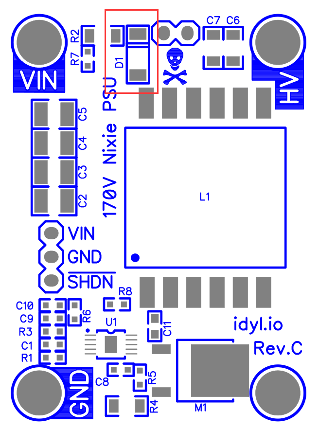
One last thing which is undoubtedly a lesson learned: don’t deviate from the norms: a few days after the process started I received an email from the fab’s agent asking for the orientation of D1. She pointed out the offender by sending me a picture of the silkscreen:

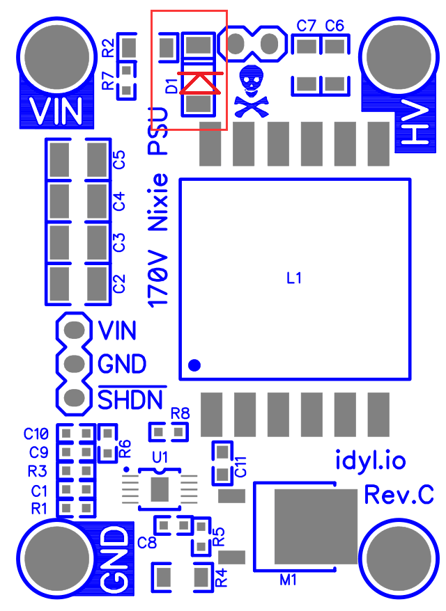
I thought my silkscreen was clear enough. The double bar at the top clearly marks the cathode of the diode, matching what you can find on a typical SMD diode. But apparently that wasn’t good enough. Next time I’ll just use a simple dot. So, using MSPaint myself, I drew my best diode as an answer:

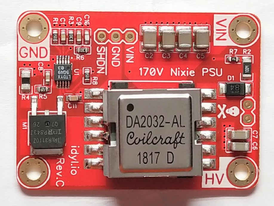
They produced one board, sent me a neat picture of it to confirm everything was in order (especially, again, orientation) and off we go!

 Tony
Tony
Discussions
Become a Hackaday.io Member
Create an account to leave a comment. Already have an account? Log In.