Now when the UI part is done I spent some time to get cylinder/tower ready to start hook up the CPU and memories to it.
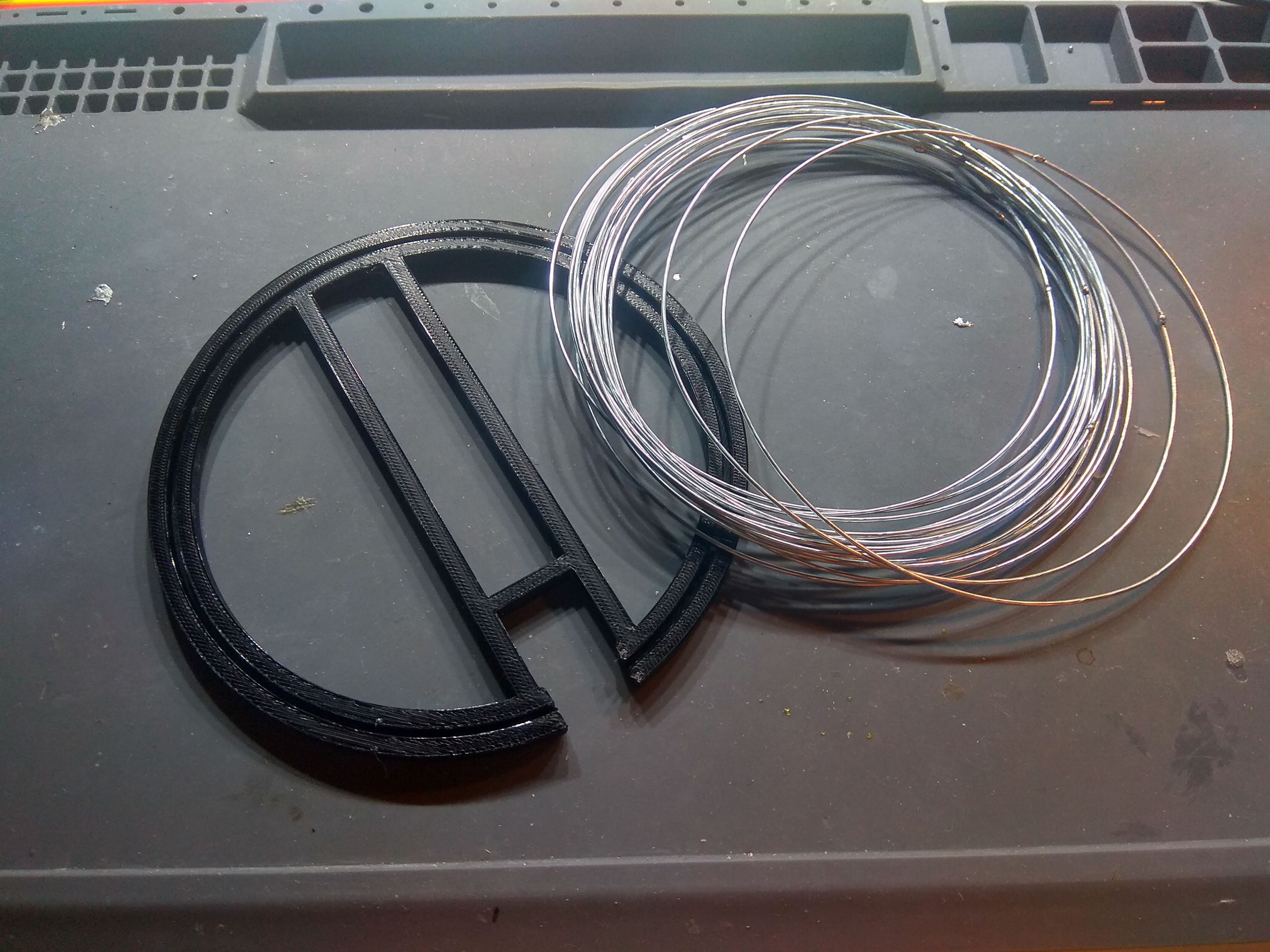
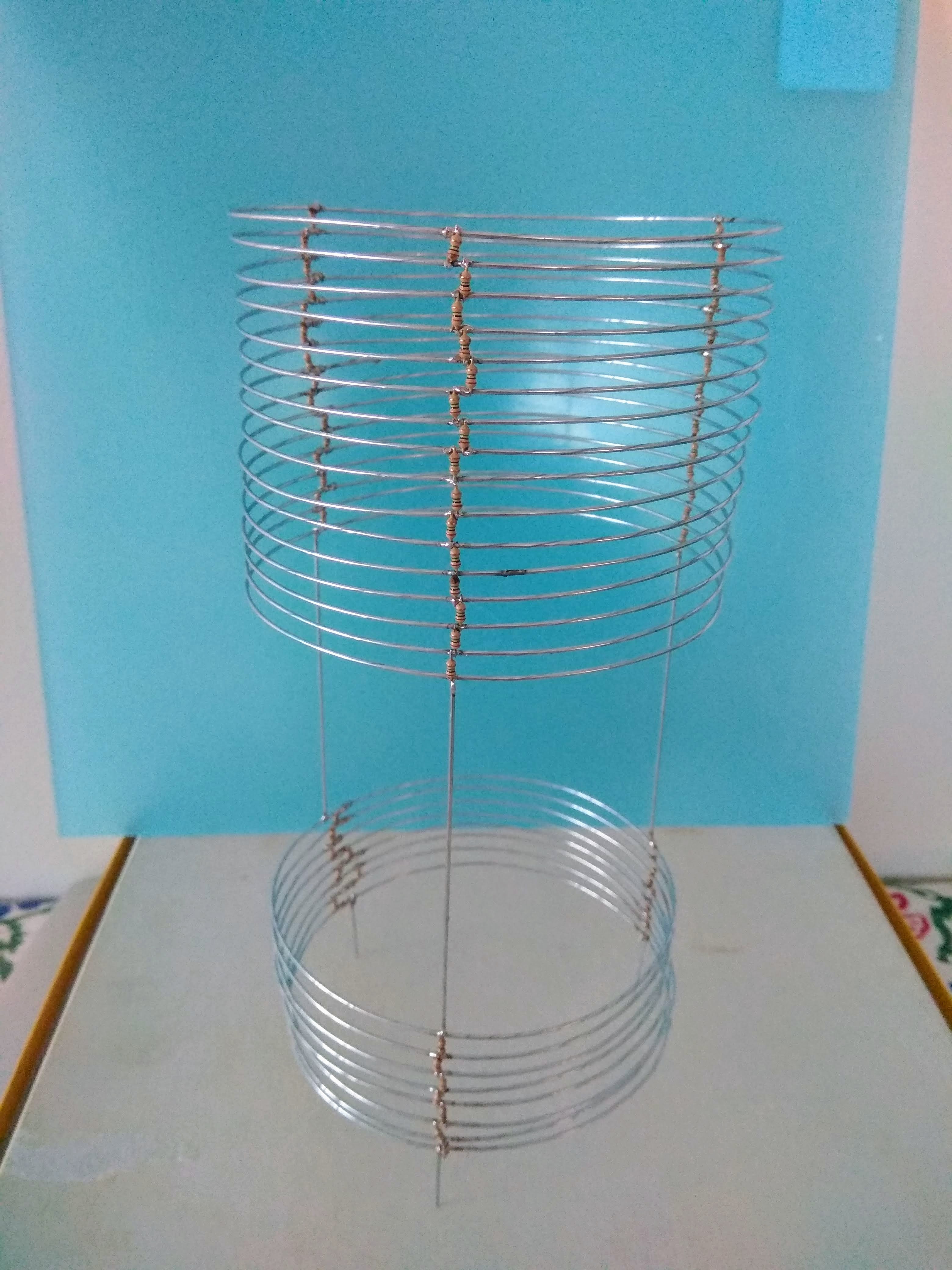
The sixteen rings was easy to make with the new jig I 3d-printed to keep the rings steady while soldering together the ends of them. (The jig reminds me of something - maybe the Quake logo?)

Now that I got some experience from soldering the smaller databus it was rather easy and fast to solder up these 16 into a decently looking cylinder.
Then I (temporarily) patched the two separate cylinders together with three wires to make some distance between the buses where the ICs will be soldered.

 matseng
Discussions
Become a Hackaday.io Member
Create an account to leave a comment. Already have an account? Log In.