 Amos
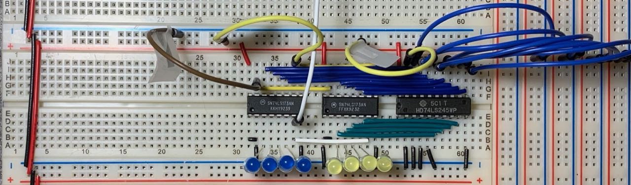
AmosI have completed the rewiring of the first register. I chose the instruction register only because it lives on the same side of the construction as the clock module. I tested the new IR and it works flawlessly. I haven't yet wired in the data bus or clock signal properly, but for now it is looking pretty good.
And for reference, the current (new) layout is below:
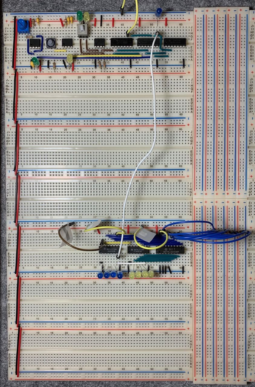
Tomorrow I plan on connecting the data bus and adding some pull-down resistors and indicator LEDs. You may notice I have 10 lines in the data bus - I am planning on using one for the clock and one for the inverted clock signal. That should make routing the clock signal a bit nicer. After wiring up the bus, I will then re-do the A and B registers and (finally) start on the ALU.
Discussions
Become a Hackaday.io Member
Create an account to leave a comment. Already have an account? Log In.