And again I got the opportunity to order PCBs, this time from PCBWay. I decided to grow the family of pins and introduce the Classic Pin in Blue. Design files stayed the same as the red one with one exception, I added the name of the PCB order (with a bad typo nicely hidden by the battery :) on the component layer to make sure that nothing got added to silkscreen of the front side. And it sort of worked, as PCBWay added an additional lot number on the component side. So the business end looks wonderful as planned. The order process is as easy and straight forward as you could wish.The order website interface is accessible here (https://www.pcbway.com/orderonline.aspx) and very easy to use. Adding Gerbers, all PCB order info, quantity and additional parameters and pressing order button is done in no time. I opted for the lead-free RoHS plating as those boards are planned to be sold on my Tindie page. PCBWay also just introduced a Gerber Viewer, which helps to control that the design files are processed as expected. The tool was not available when I ordered, but I just gave it a test with my data and it looks very nice. You can choose between layer and board view. See below: This seems to be an open source tool and good on them that they mention Mike Cousins as the creator (Kudos to him for living the open source spirit).
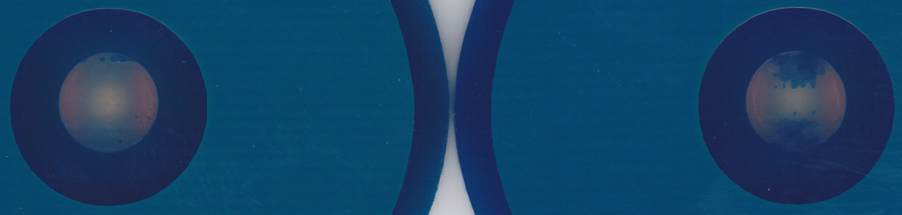
The board quality is very good, all pad and silkscreen features came out aligned perfectly as designed. Silkscreen resolution is very high and good enough for artistic features. Soldering was very good, the lead free plating was very good to work with. And it works and looks beautiful. On a few boards, the soldermask was flowing into the big opening on the other side of the reverse mounted LED. I have to rework them, not big deal. For the shipping option I picked E-Packet (10-15 days) and it arrived through Canada Post after 10 days. Perfect. I am really happy that PCBWay gave me the opportunity to testdrive their service and the project fulfillment experience was flawless. If you want to know more about their services, please contact luna@pcbway.com.
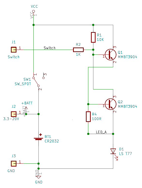
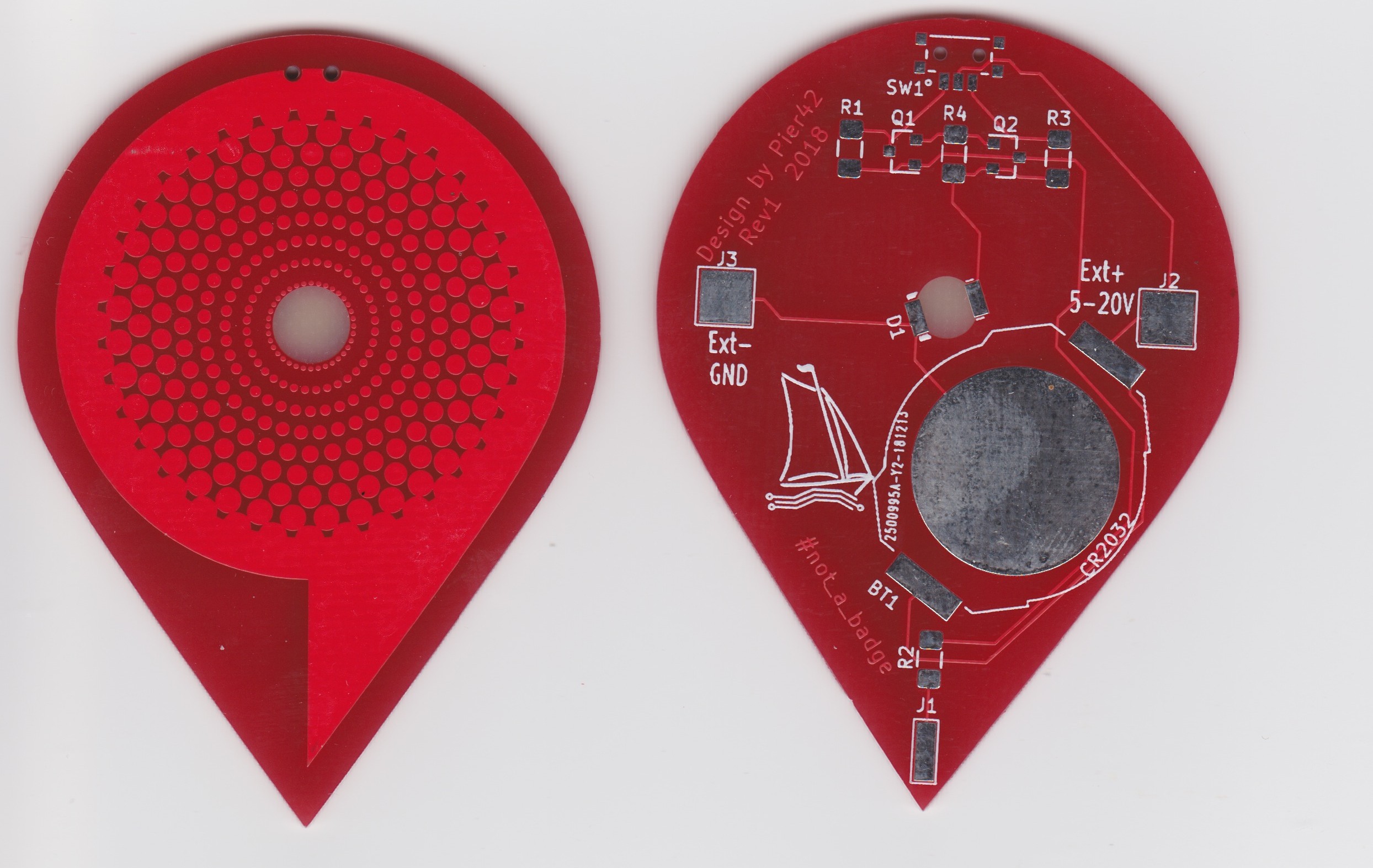
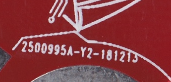
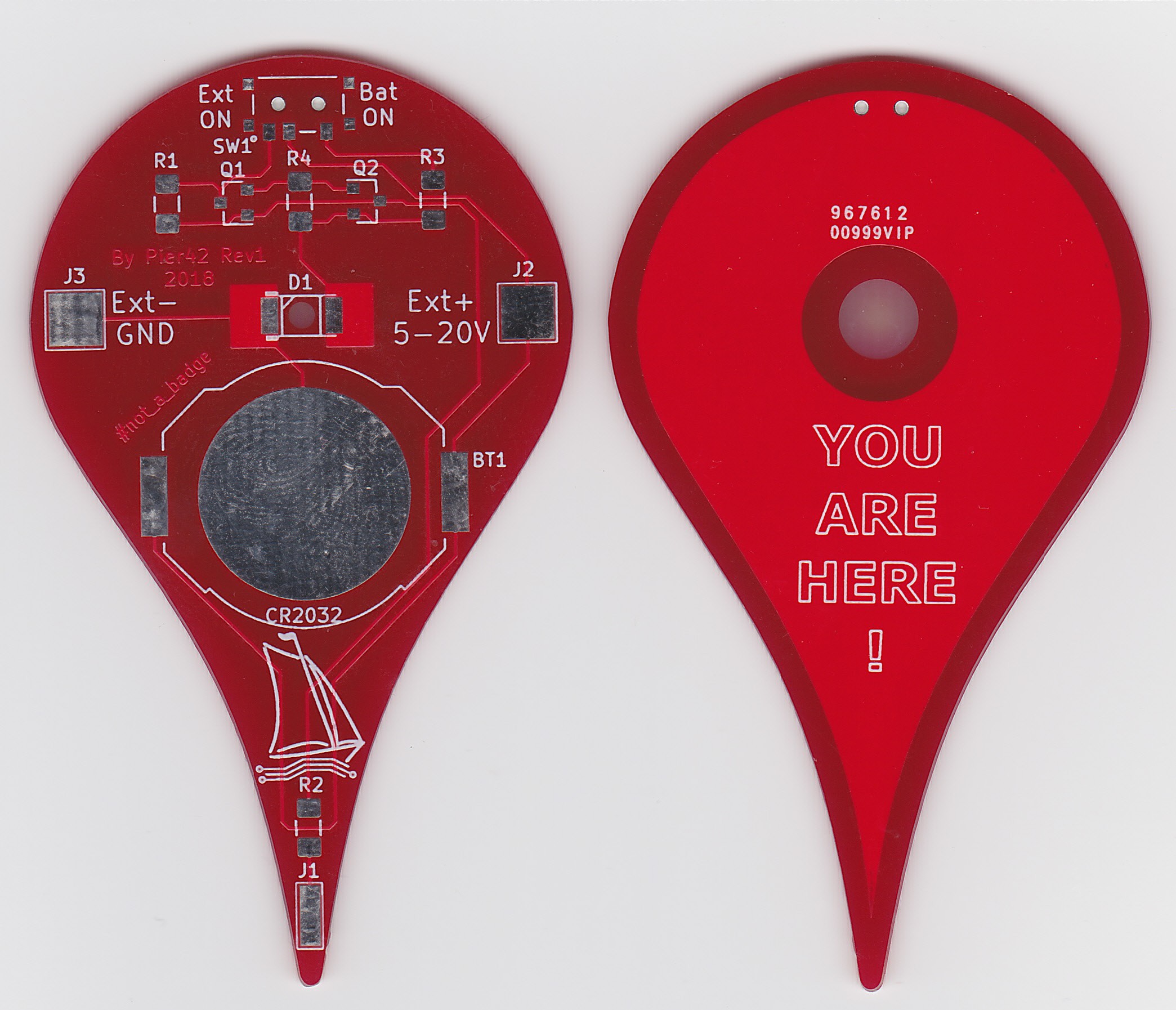
JLCPCB offered me to test their PCB service, so here we go. The test subject will be my 2nd installment of my artistic PCB theme named 'You Are Here'. This time a modern take on a location pin that shows up on many location features all over our modern life. Quoting and ordering through the JLC web interface is as painless a it gets. You upload a Gerber zip archive, pick your PCB parameters and get an instant price including shipping and an estimated delivery time. It starts at less than 3.00CAD for green boards 10cm x 10cm in standard 1.6mm thickness. My board was slightly more expensive as I opted for red soldermask and leadfree HASL finish, cause the boards might become my second batch of pins to be sold on Tindie.
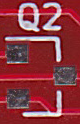
The quality is excellent, all features came out exactly as I had them designed. The PCB layers are aligned perfectly, no overlapping of soldermask or silkscreen onto the pads.
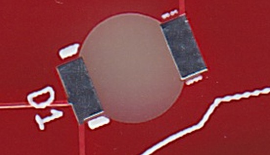
Silkscreen resolution is adequate, the rastering only starts showing up slightly on angled lines.
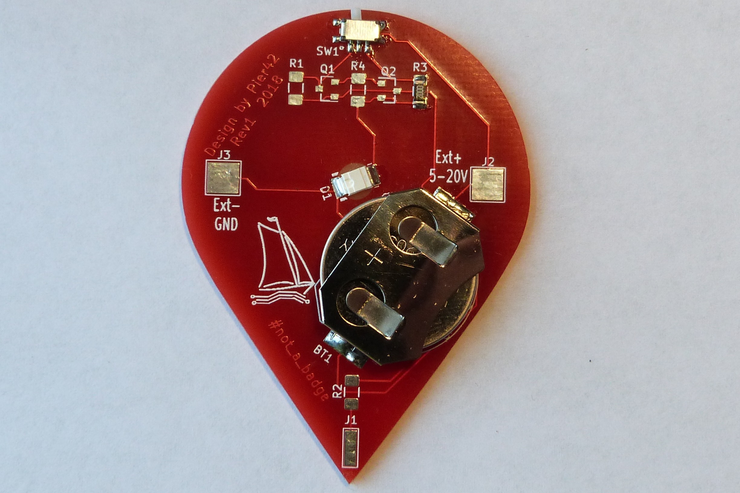
Everything was very good to be soldered, even with the lead free HASL finish, I just increased the temperature of the iron by ~30 deg.
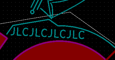
One very special feature that JLC is offering, is the location selection of the serial number that they are printing on the board during manufacturing. If you put a text string called 'JLCJLCJLCJLC' on the desired location on the board, they are going to use it for the serial number. This guarantees visible features to be not altered at all. It is even possible to put this string under a component body and then it will not be visible at all. This is especially helpful for artistic PCBs that should have at least 1 side exactly as designed.
Shipping through DHL was without any problems, the boards arrived from China to Canada in 7 days after the order was placed.
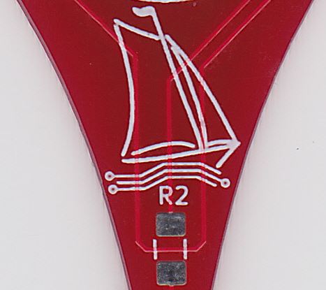
I got the opportunity to order PCBs from Seeed Studio through their Fusion PCB service. As you can see from the pictures it is a more artistic than complicated PCB and the quality is outstanding. I designed the board with relaxed spec of 7/7mil trace width/spacing and 0.3mm hole size, which fit perfectly in the most price competitive option. Registration of all layers, including soldermask and silkscreen is excellent, everything is centered and no unwanted overlapping onto the pads. Also the PCB outline is routed all the way around and the break-off tabs are not noticeable at all.
Also the silkscreen resolution really good, virtually no steps are visible on angled or curved lines, which makes it very usable for advanced graphics.
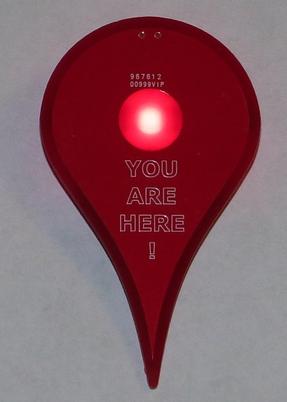
Pricing is competitive when using the HASL option and the standard 2-layer 100mm x 100mm size restriction. I went for HASL lead free, as the boards are intended to be sold in my Tindie store once all parts arrive. The circuit is operational with a mock-up LED and the FR4 substrate acts as a nice diffusion layer for the light.
I opted for shipping through DHL which took 4 days from China to Canada to the local depot, and another 4 days for the local contractor to deliver because they ignored my instruction for pickup at the depot. This is not controllable by anybody at the shipping or receiving end, so it was just bad luck for me. Other shipping options are available.
 MagicWolfi
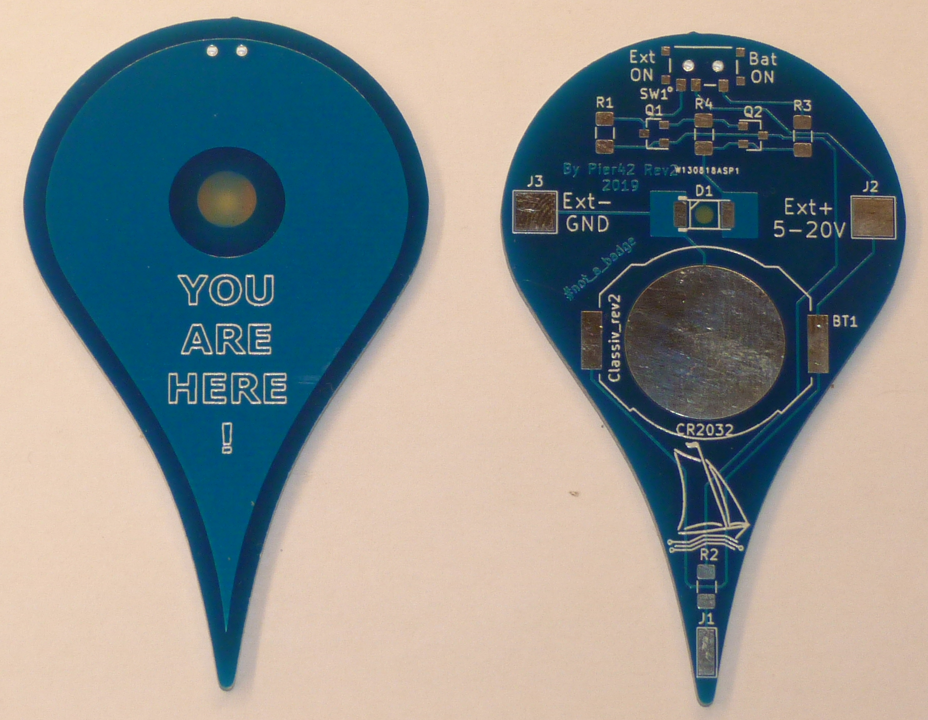 The order process is as easy and straight forward as you could wish.The order website interface is accessible here (
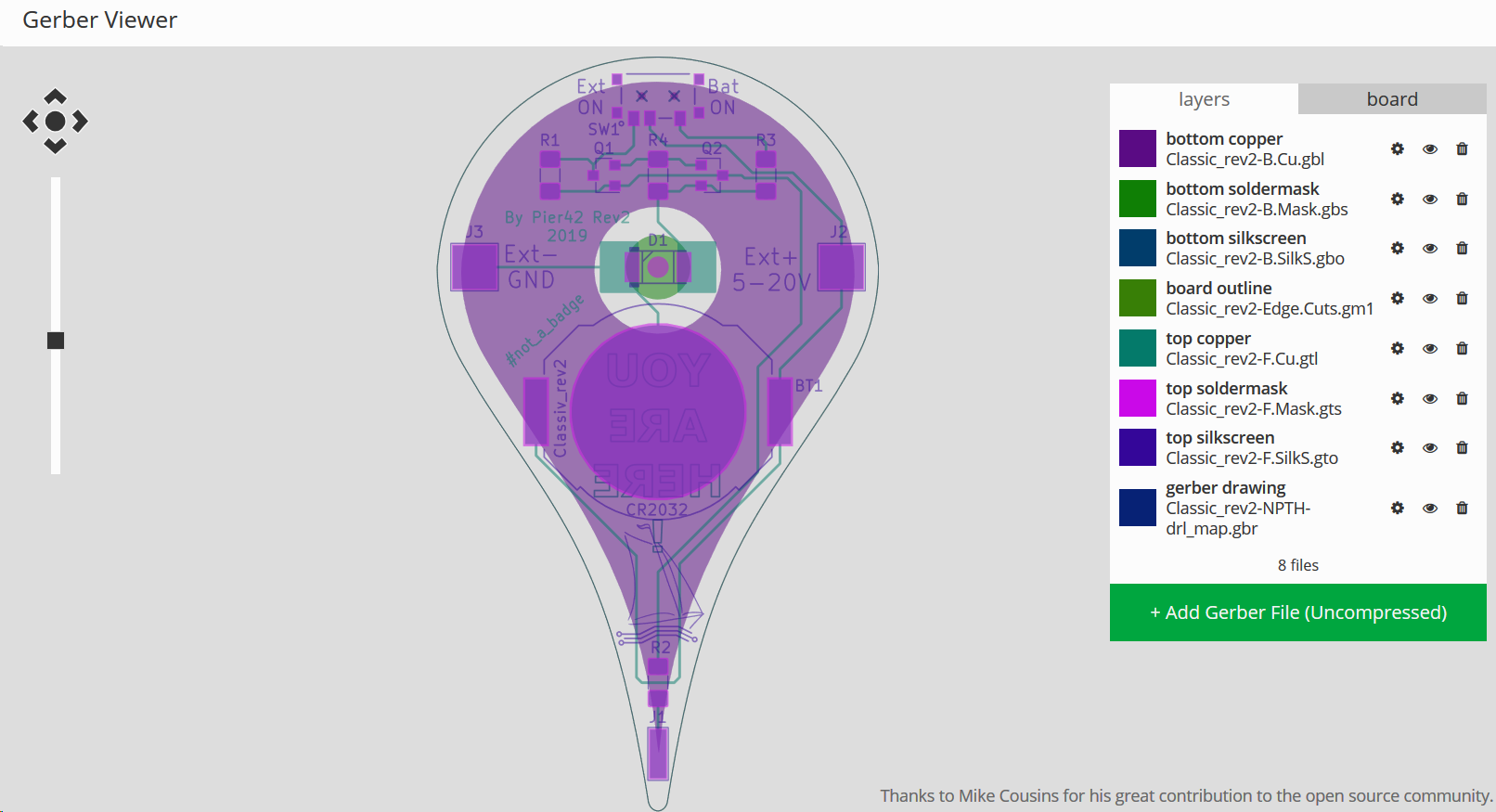
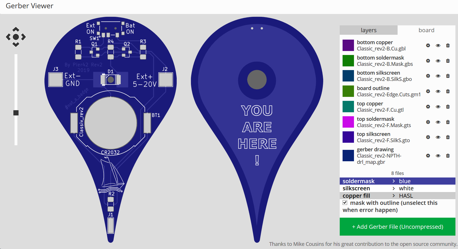 This seems to be an open source tool and good on them that they mention Mike Cousins as the creator (Kudos to him for living the open source spirit).
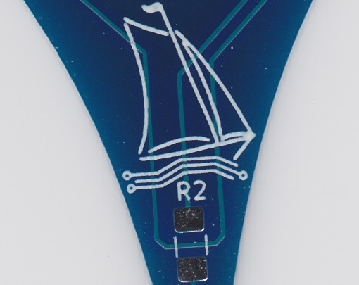 Soldering was very good, the lead free plating was very good to work with. And it works and looks beautiful.
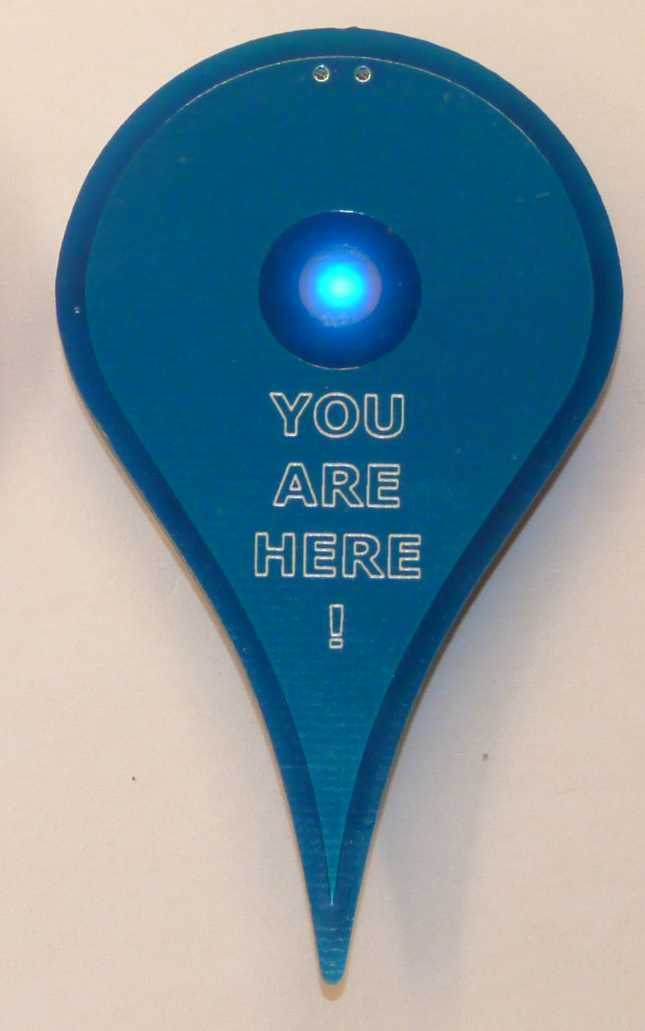
 For the shipping option I picked E-Packet (10-15 days) and it arrived through Canada Post after 10 days. Perfect.