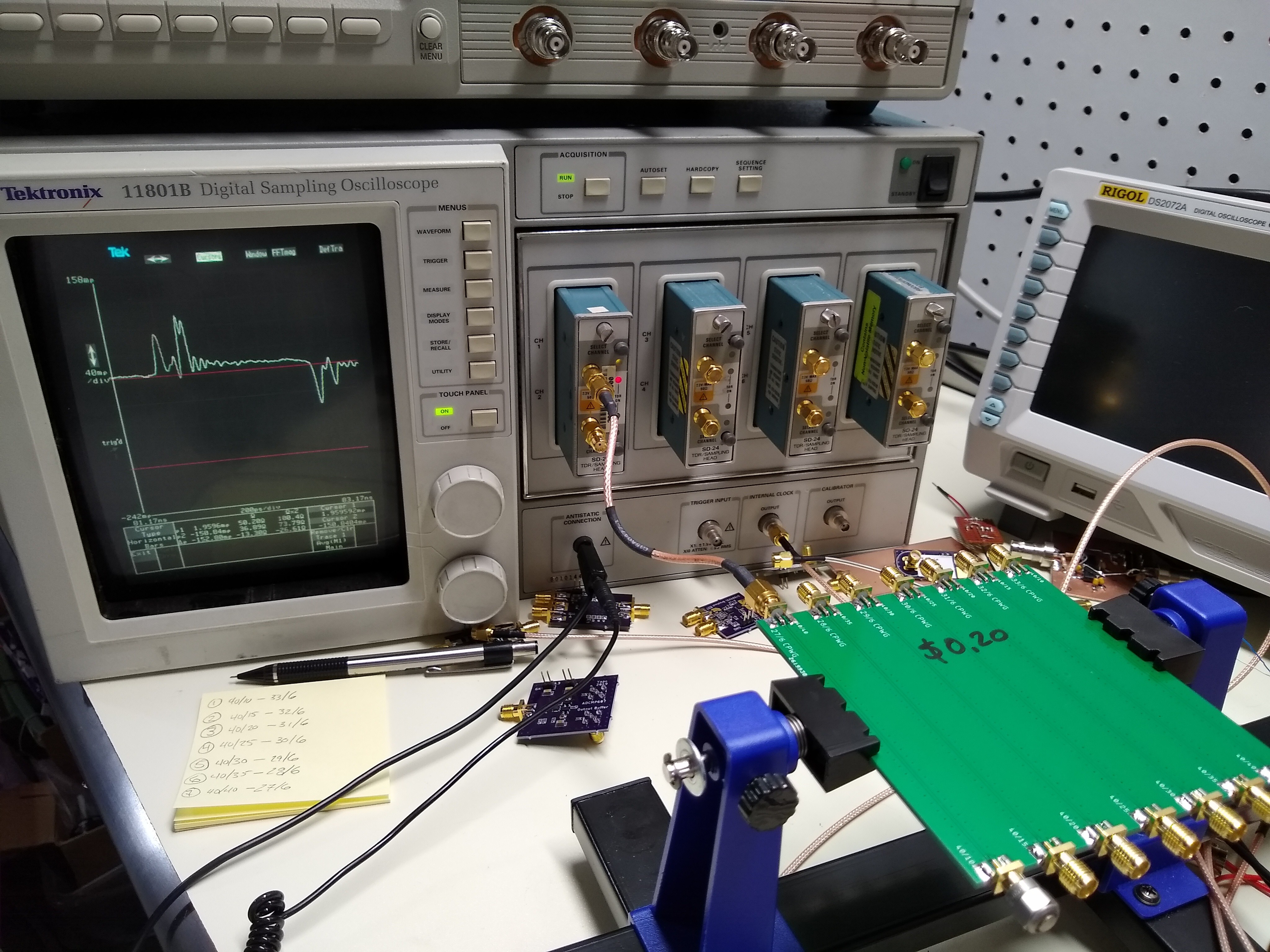
I send out another batch of 2-layer PCBs to test different coplanar waveguide geometries and SMA end-launch connector footprints. There are seven different CPWG widths and seven different footprints on the PCB. I populated one with $0.20 ebay SMA connectors for the first test. I'll compare with $2 name-brand connectors next, then maybe some good ones.

It took two tries to make the boards this time because of sloppiness and an Eagle bug. When you copy a single via in Eagle, you get another one on the same net. When you copy more than one via at once, they all end up on another net, for instance GND1, GND2, etc, which aren't connected to anything. I quickly cut & pasted the stitching vias on either side of the CPWG traces, and didn't notice this before sending out the first batch of boards. This PCB was too simple to bother running DRC, which would have caught it right away :-(
Results
Here are the measurements, summed up in an animated GIF. This format really shows how the impedance changes with the trace parameters. In this case, I kept the CPWG gap fixed at 6 mil, and varied the trace width. A common geometry for 50-Ohm CPWG on 2-layer 62-mil PCBs is 32/6, a 32-mil wide trace with 6 mil gaps on either side. I found that when covered with soldermask, the characteristic impedance of such a trace is typically too low - a narrower trace is called for.

The upper cursor is at 50.91 Ohms, and the lower at 49.3 Ohms. The long flat area is the CPWG trace, and you can see the impedance increase as the trace width is reduced. The best match to 50 Ohms is between 30 and 31 mils. 30.5 might be a good width to use. Of course, this is going to vary because of the somewhat random dielectric constant of FR-4, but at least it's a real data point.
SMA Connector Footprint
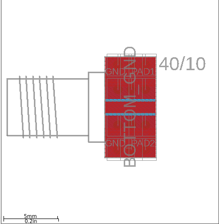
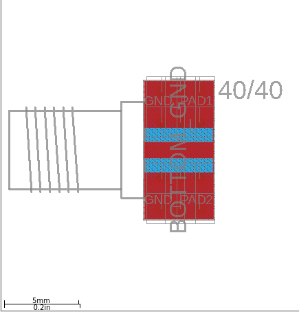
The other variable in this test is the shape of the SMA connector footprint. The footprint consists of a 40-mil wide pad to solder the SMA connector pin to, with gaps on either side. Because the pin and the connecting solder introduce capacitance to the structure, you have to widen the gaps to maintain 50-Ohms. Here are two of the footprints, with 10-mil and 40-mil gaps. These views don't really show the vias stitching the ground planes on the top and bottom layers. The plane is solid on the bottom layer.


In the animated GIF, you can see for the 40/10 footprint with 10-mil gaps, there's a very large capacitive (negative) dip at the footprint. As the gaps are increased, you eventually get an inductive (positive) bump. In between, at around 40/20, you get a minimum bumpiness at the footprint. There's still some wiggling of a few Ohms, and a large inductive bump before the footprint (inside the connectors). These are $0.20 SMA connectors, after all, which I don't expect much from.
Next Up
I'm going to populate another PCB with $2 connectors and see what they look like.
 Ted Yapo
Discussions
Become a Hackaday.io Member
Create an account to leave a comment. Already have an account? Log In.