The first attempt of bringing this to life was a fail. I toasted some chips and had a lot of shortcuts between the unisolated wires. I could not find a way to find all the errors in this mess of wires. Therefore this project had to sit on my shelf fore quite a while... :-)
But after more than a year I was in the right mood and decided to give it a second try.
The circuit around the Atmega was working, It was possible was to communicate and upload software. I removed most of the other stuff and started the wiring (nearly) from scratch.
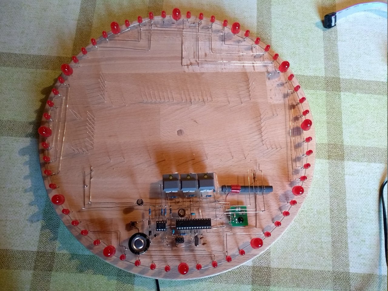
This time I did a lot more planning before starting the rewiring. I tried to divide the circuit in several modules and assembled the modules separately. After the assembly of each module I tested it thoroughly for short circuits and any other wiring errors.
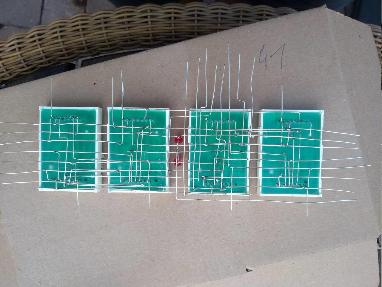
This is the display module with rows and columns (not completely ready). The rows and column wires connect to the "poles" in the picture above. It is rather easy to test a sub module of this size and correct the unavoidable errors.
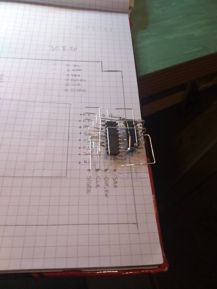
One of the row drivers...
Discussions
Become a Hackaday.io Member
Create an account to leave a comment. Already have an account? Log In.