-
The "MP/M experiment"
07/19/2019 at 07:32 • 0 commentsThis is a crazy experiment that I've done using my own HW, just because I was curious to see a MP/M system running in a "real" situation with 4 concurrent terminal/users.
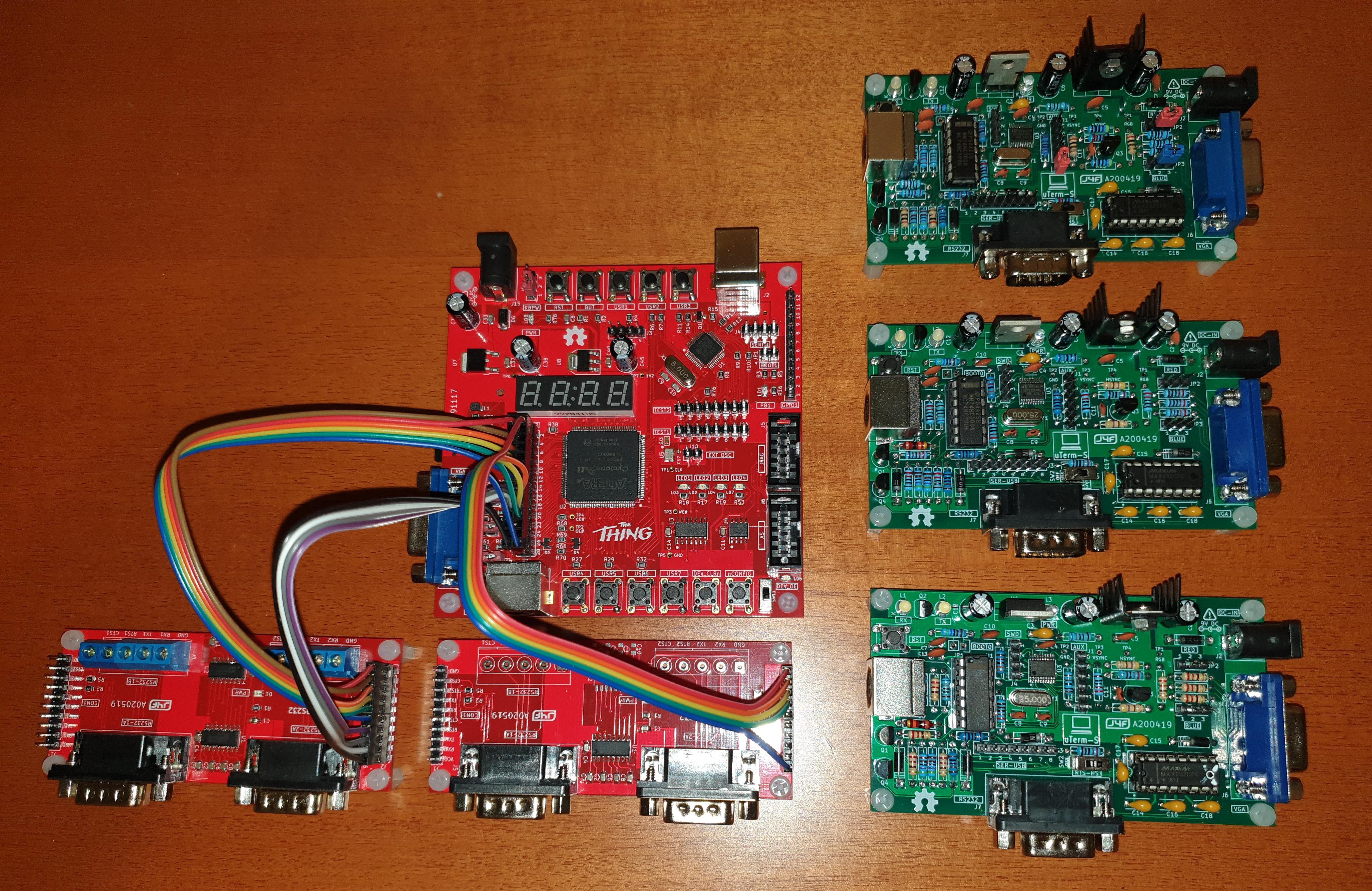
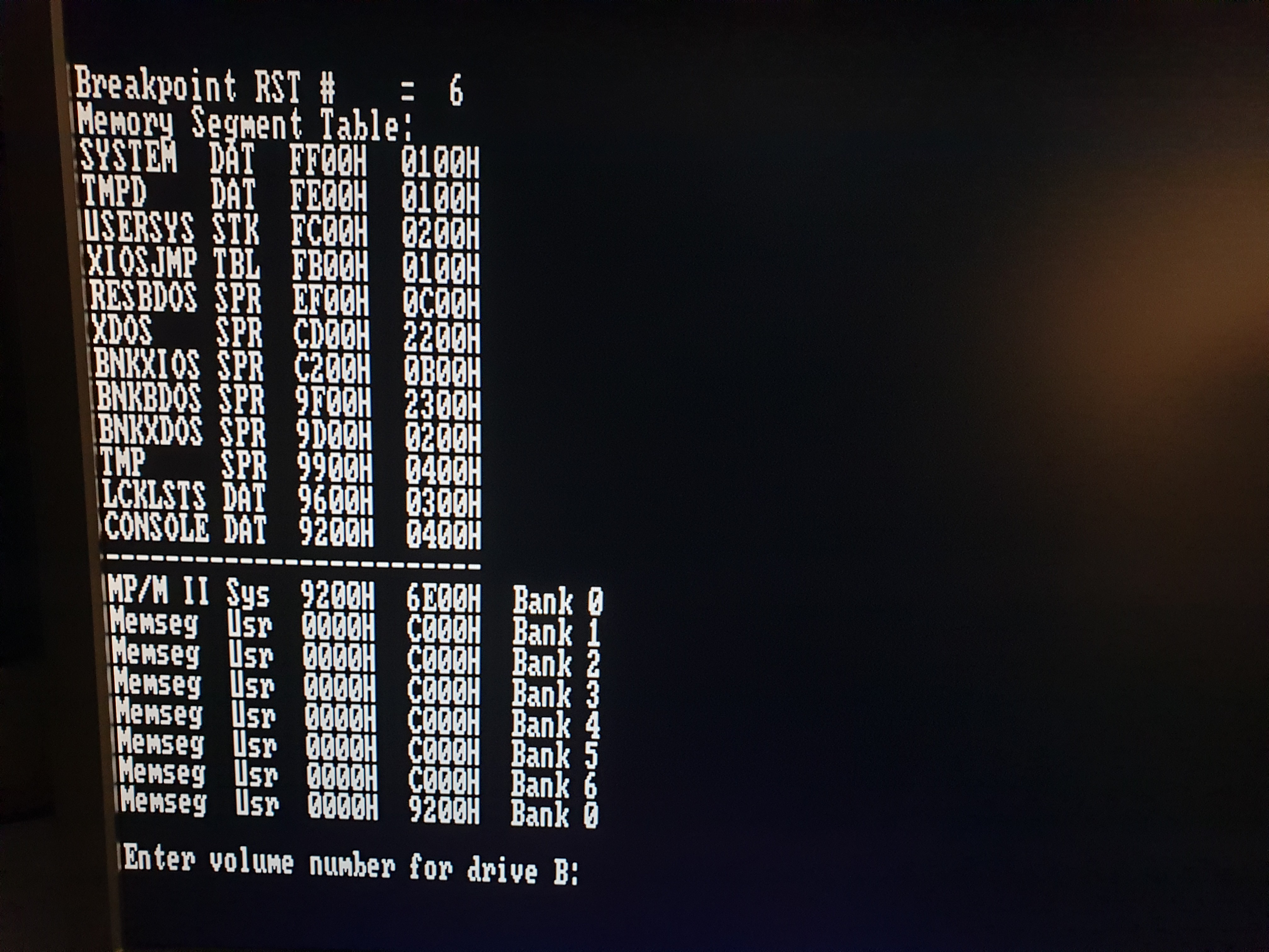
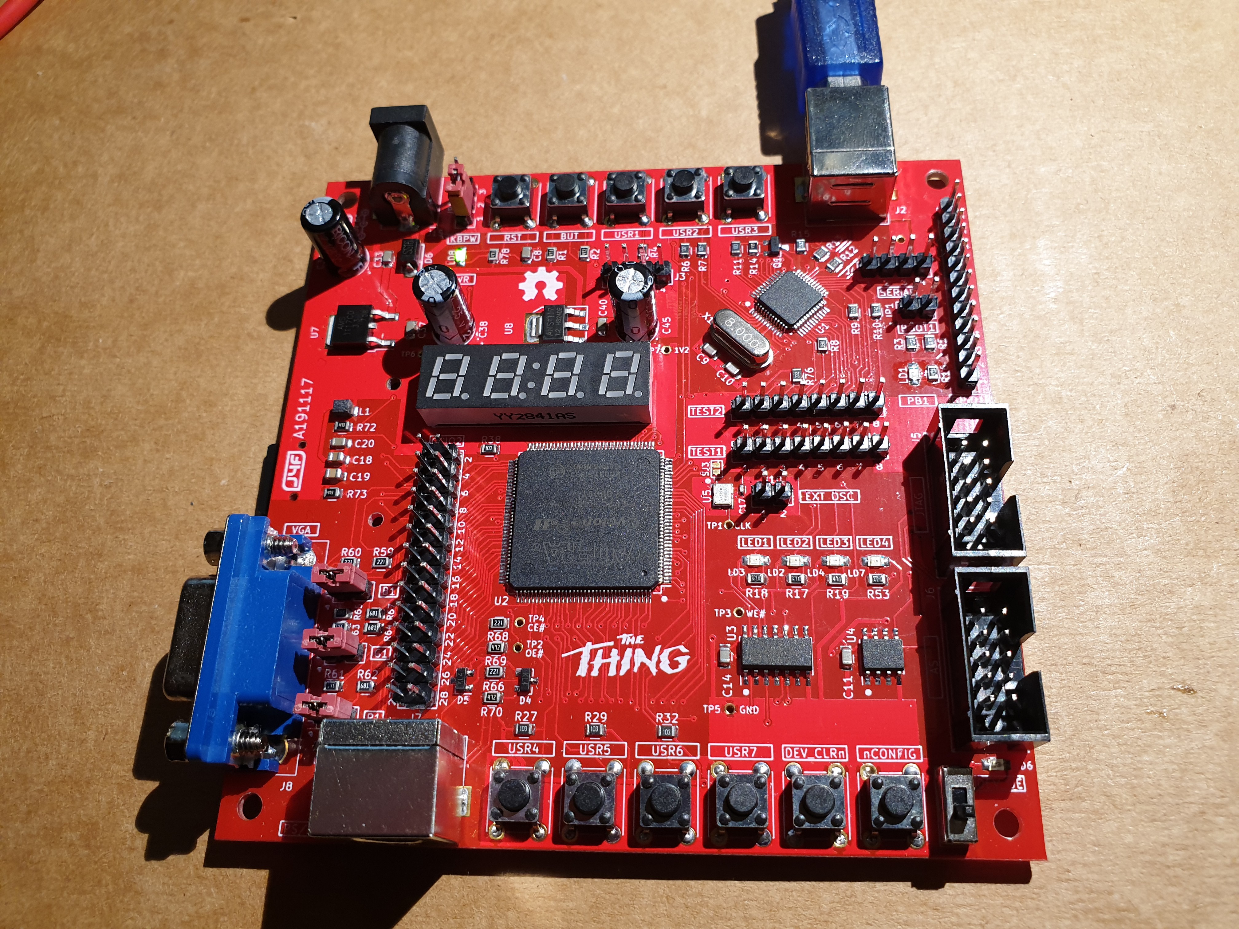
The FPGA board runs a VHDL Z80 Multicomp with MP/M 2.1, HD on SD and 4 serial ports (I've ported it from the Retrobrew site adding the needed modifications):
![]()
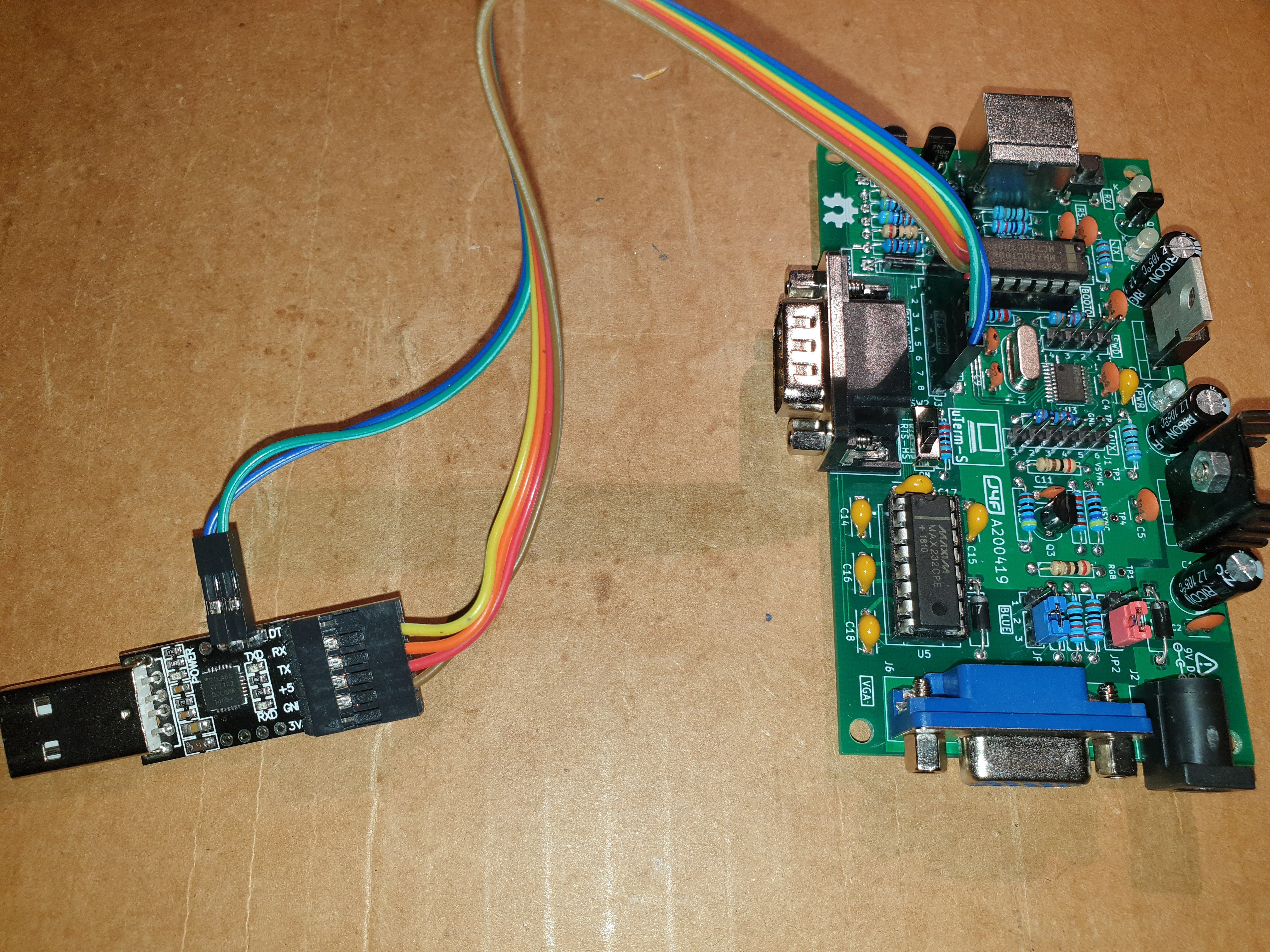
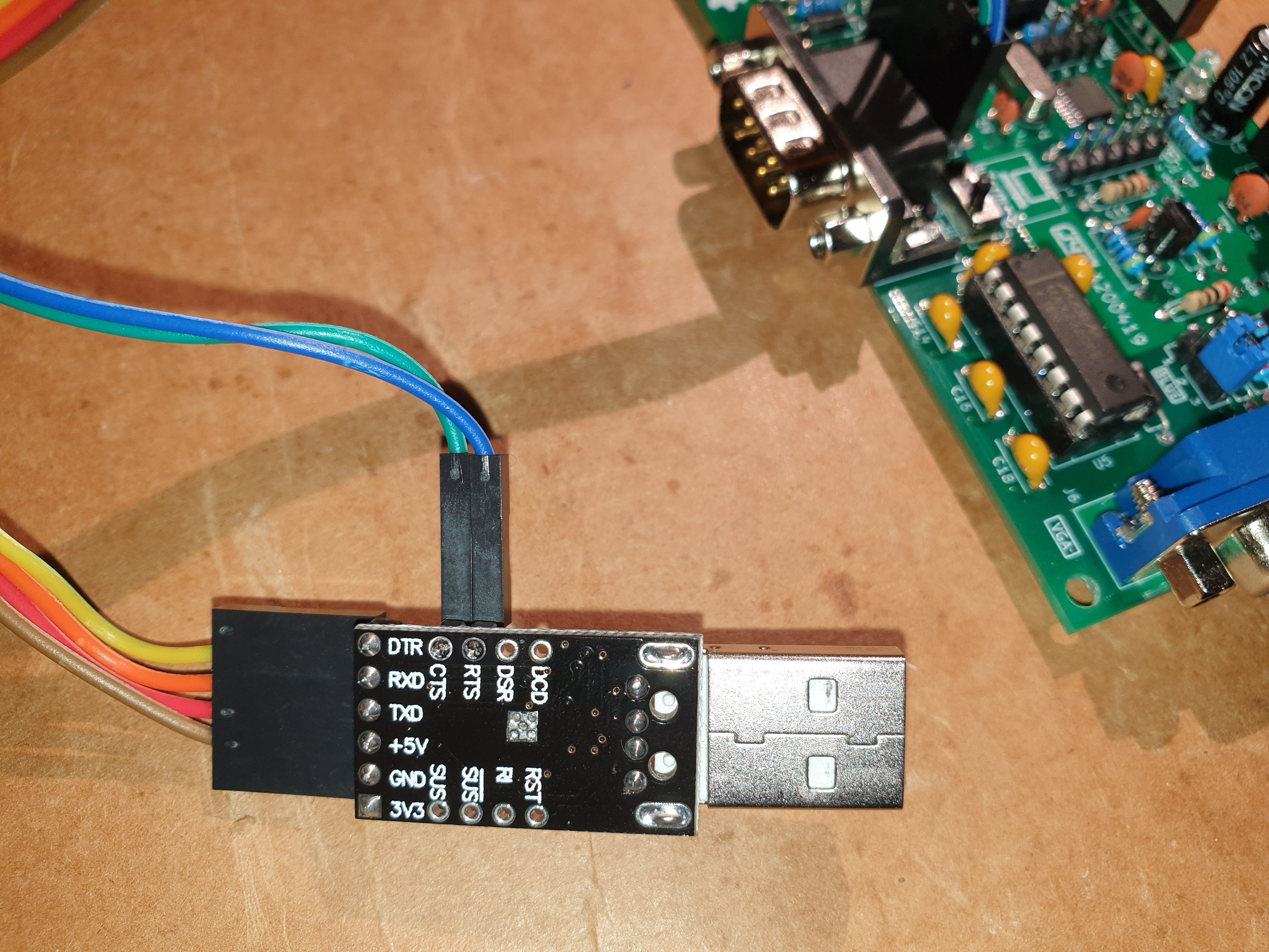
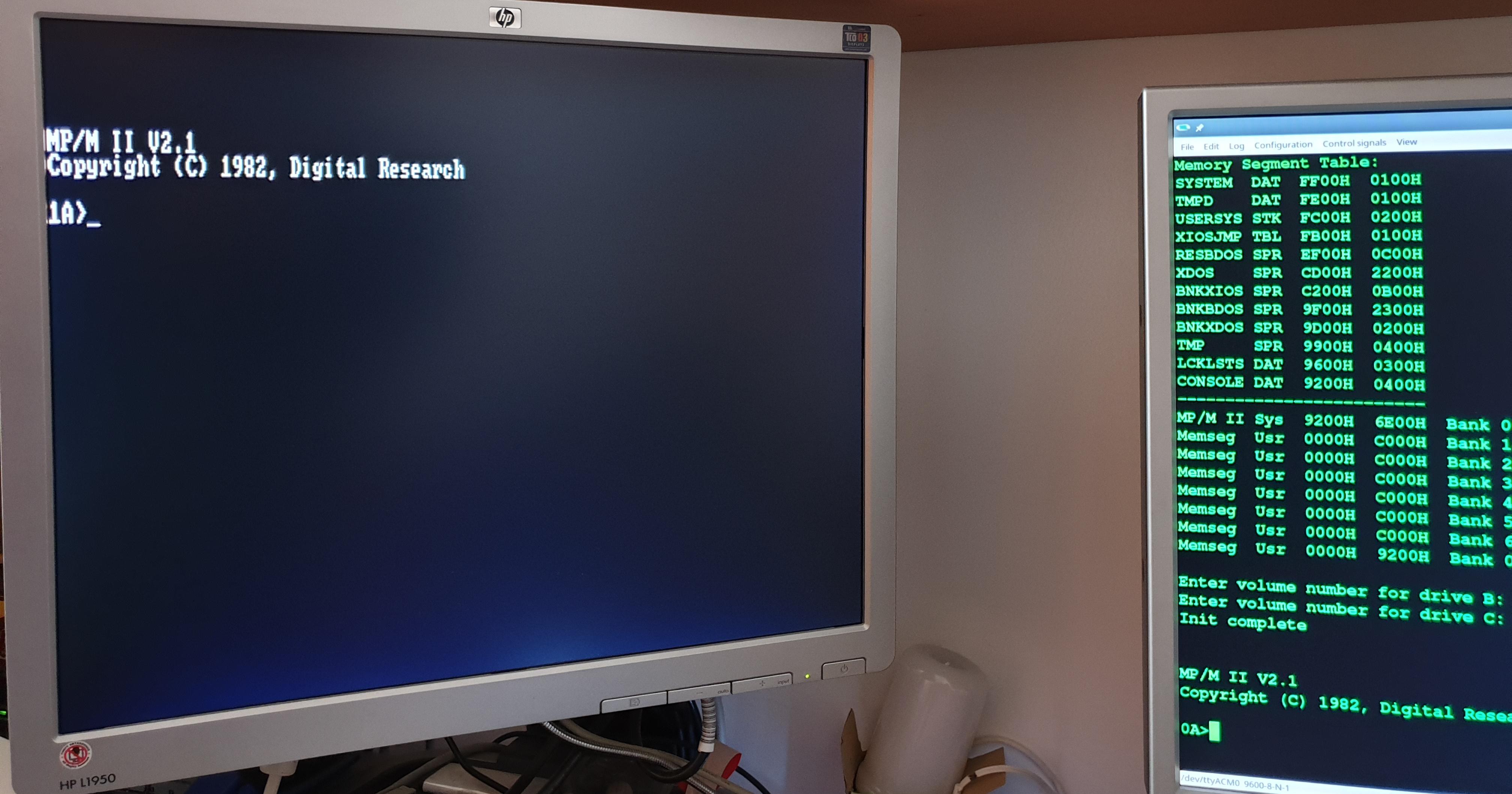
One FPGA serial port (Serial 1) is connected to the STM32 MCU inside the board, and the STM32 runs a "sketch" to act as a serial-USB bridge. So the USB connector is used to power the board and also to connect the Serial 1 port of the Multicomp (inside the FPGA) to a terminal emulator (on a PC):
Here the setup I've used:
![]()
and the video:
-
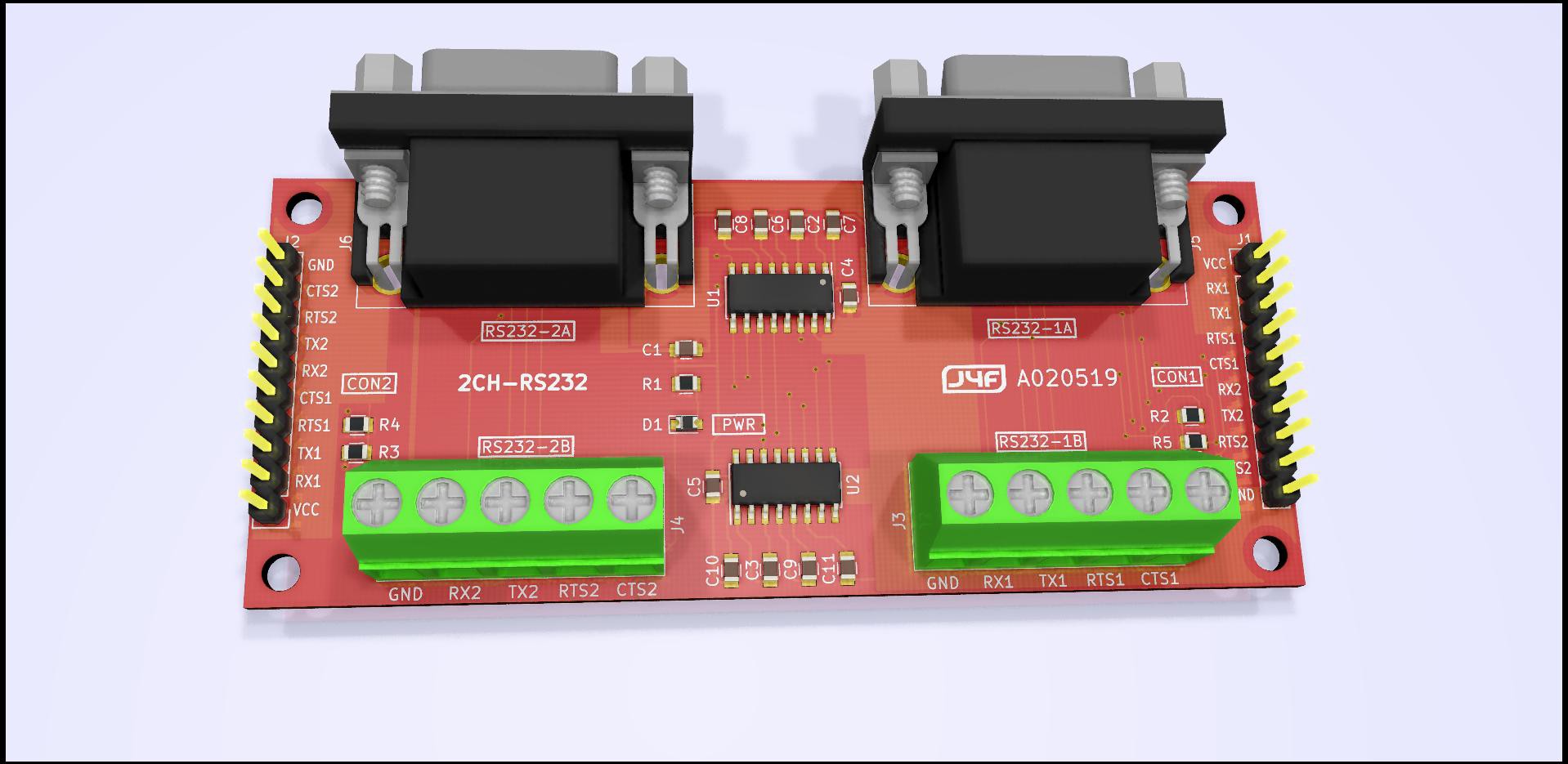
Dual-channel RS-232 adapter board is out!
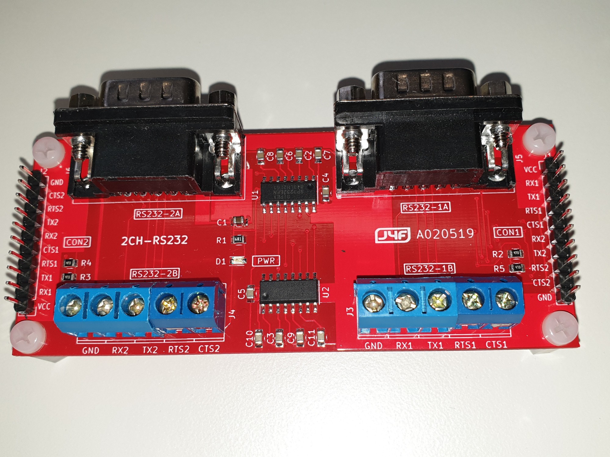
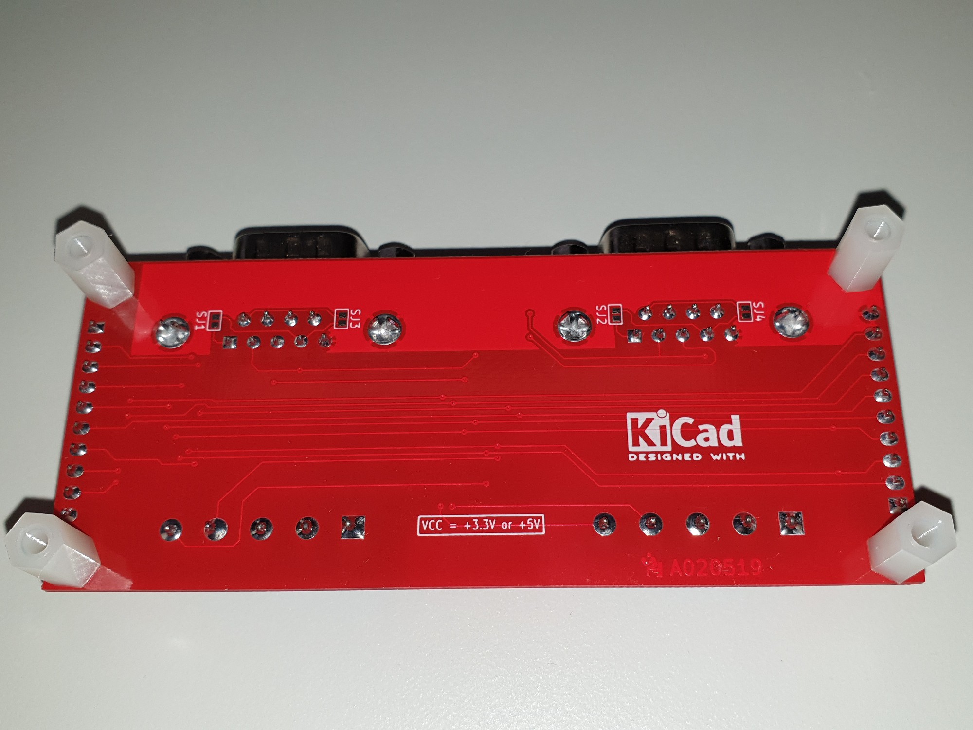
07/16/2019 at 11:54 • 0 commentsThe dual-channel RS232 board is out. All the details here.
![]()
This board is intended as a RS-232 level adapter for Multicomp with multiple serial ports.![]()
-
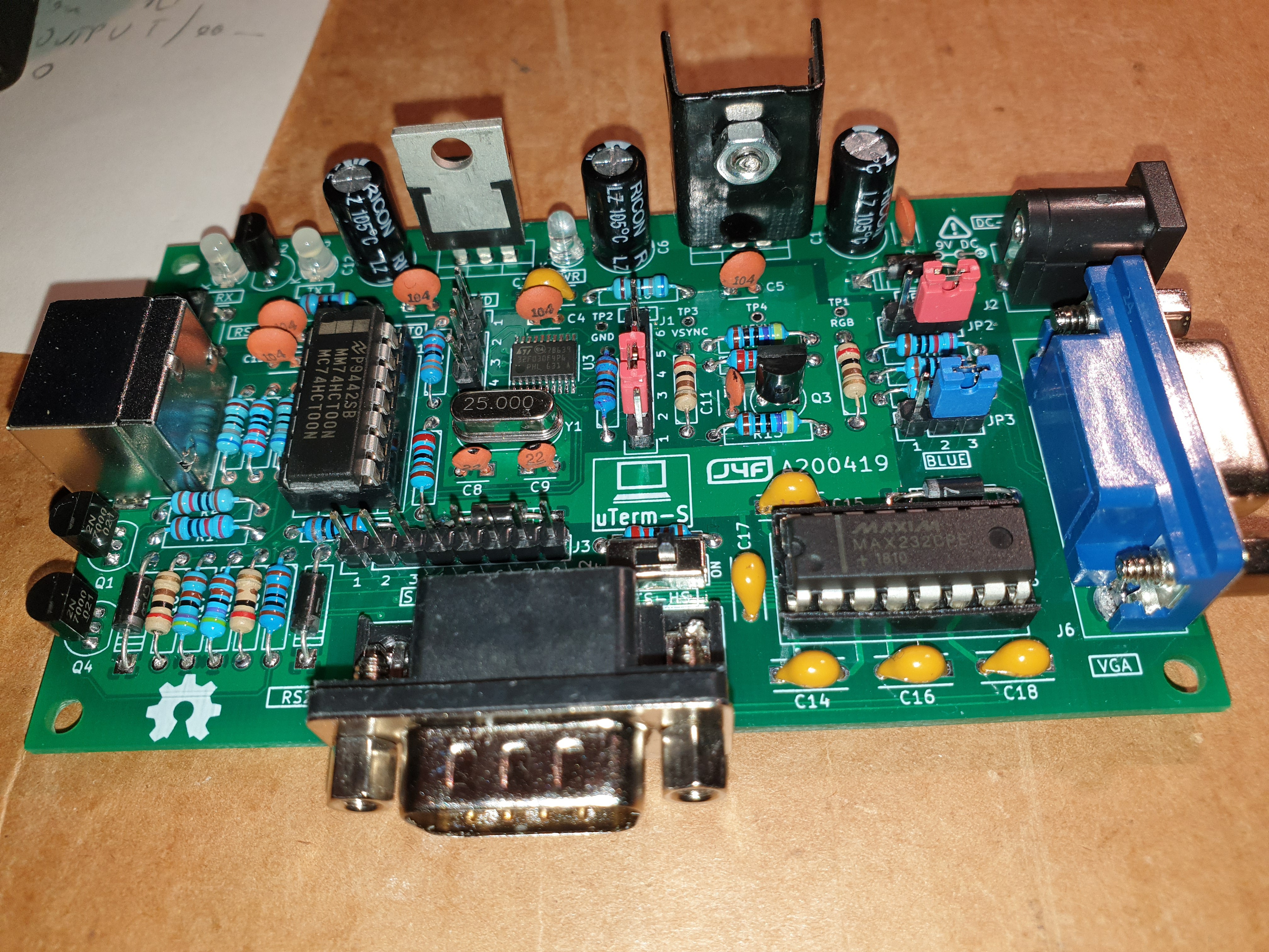
uTerm-S preview: a VT100-like terminal for multi-user OS
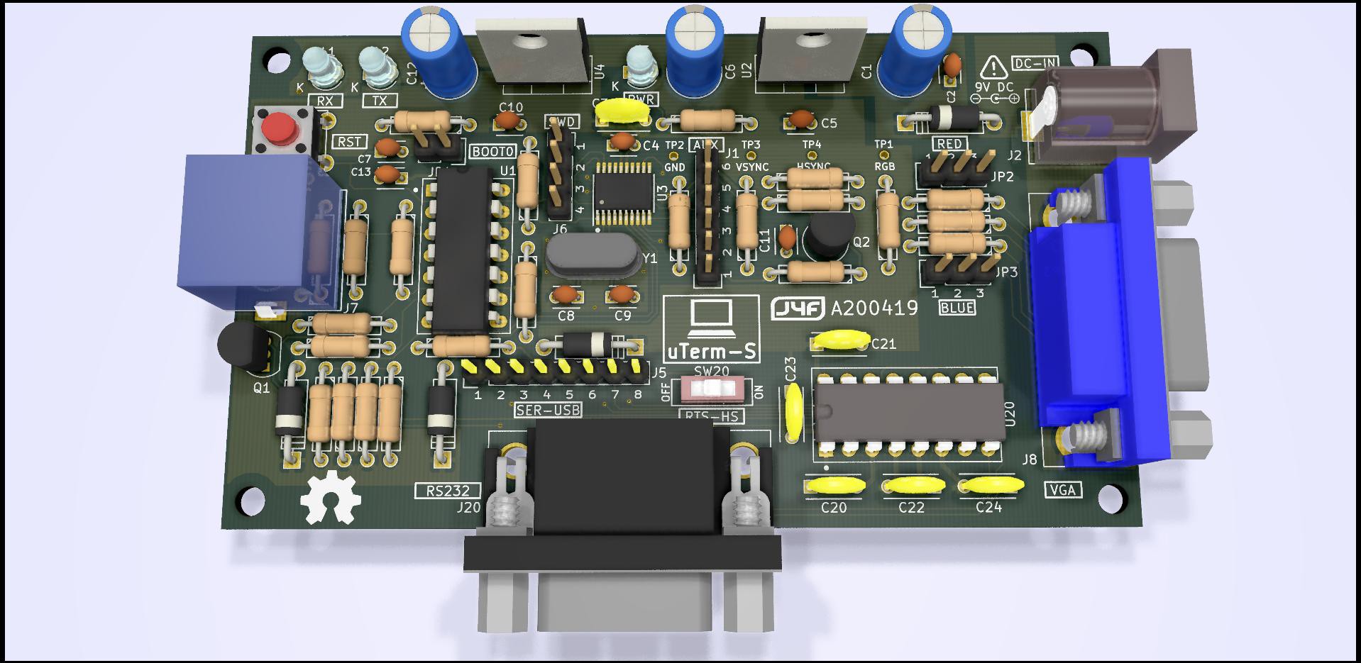
04/24/2019 at 07:31 • 0 commentsWanting to test some multi-user MP/M configurations, I've decided to make a VT100-like "stand-alone" terminal starting from the uTerm, the VT100 terminal for the Z80-MBC2 board.
I've decided to use THP parts (of course the STM32 is SMD only...) so it may be easier to build for others "retro" stuff too.
Here a first preview of the uTerm-S. In this version the "transparent" serial-USB port can manage the RTS/CTS HW handshaking (the RTS/CTS signals must be present on the serial-USB adapter):
![]()
Of course this is not enough. An other board must be done with at least a 4-ports (for 4 users/terminals) serial RS232 adapter for the "The Thing" board...
...or a couple of 2-channels RS232 adapters with both DB9 or screw connectors, and two specular TTL connectors (J1 and J2) so I can rotate the board by 180° and choose the most handy position:
![]()
-------------------------------------
Now testing the "stand-alone" VT100 terminal with RS232...:
![]()
...with the RTC/CTS handshaking on the "transparent" serial-USB connector:
![]()
![]()
-
Multicomp preview...
04/07/2019 at 19:06 • 0 commentsHere is some previews of Multicomp VHDL I'm currently porting and testing. Here a Z80 system running MP/M 2.1 (a multi-user time-sharing OS for the Z80 CPU):
![]()
...and here a session using a simple sketch for the STM32 to use it as a serial-USB bridge attached to a VHDL serial port on the FPGA:
![]()
In this way it is possible use The Thing with only the USB cable, connecting it to a terminal emulator on a PC:
![]()
Here MP/M 2.1 with two concurrent users, one connected to the local VDU/Keyb and the other connected with a VHDL serial port "redirected" to the STM32 serial on USB (using the UART "bridge" sketch on the STM32 and managed by a terminal emulator on a PC):
![]()
And here playing Gorilla:
Stay tuned...
-
Multi-functional display/leds/keys custom controller. Project example
03/06/2019 at 15:30 • 0 commentsThis is a ready to use example of a custom "multi-functional" controller for a 4 digits 7-segments led display (single segment "graphic" drive mode with digits multiplexing), plus 3 status leds, plus 3 push buttons, using a bidirectional data bus (DATA_0-7) and a register selection bus (SEL_0-2). The command signals are an active low write signal (WR_EN) and an active low read signal (RD_EN). The behavior is very similar to a SRAM device.
To make things easier, in this example it is used the schematic editor and the 7400 devices family library, but note that this is not the best way to use a FPGA (the "right way" is to use VHDL/Verilog languages...).
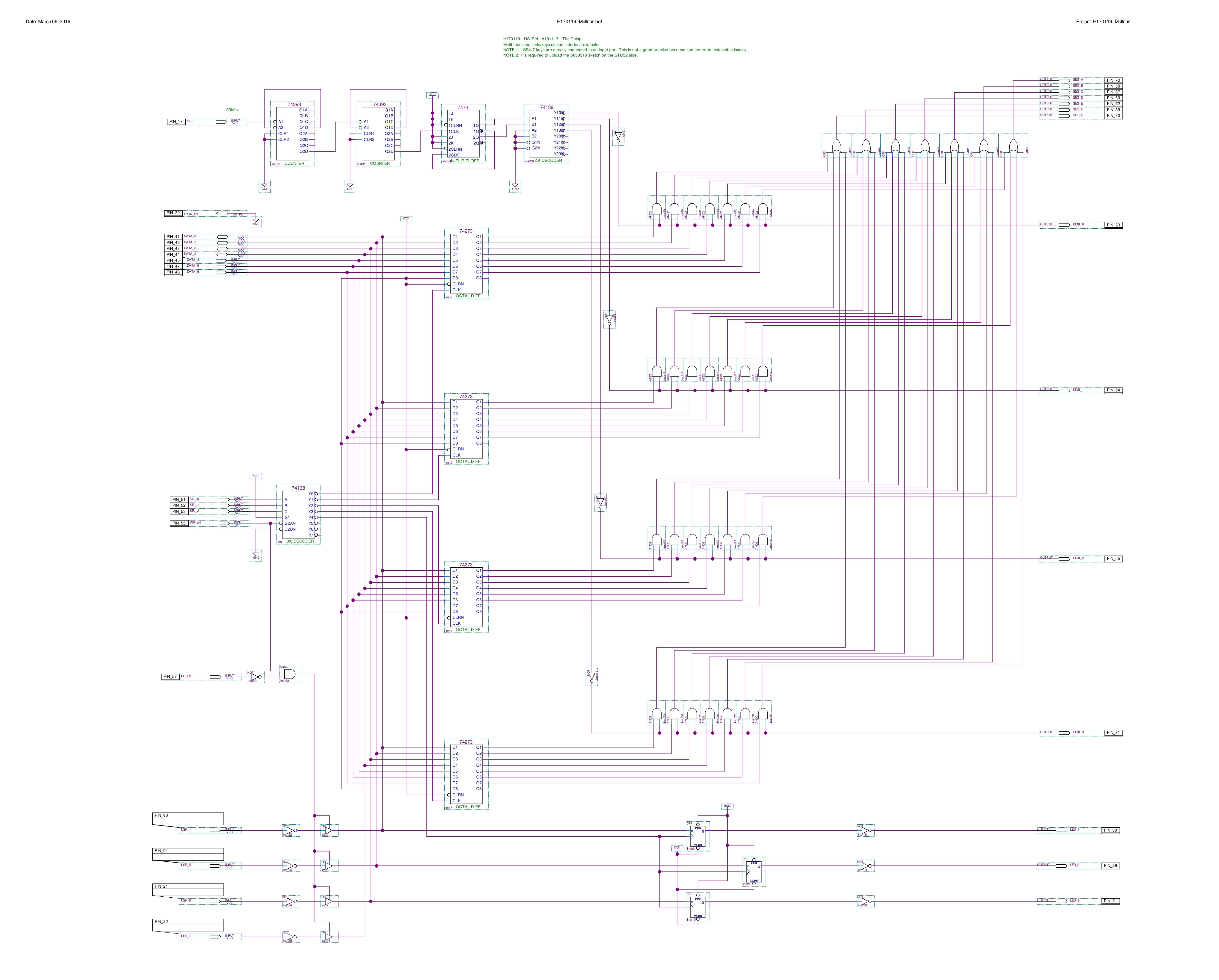
The schematic is the following (this is an Hi-Res image. You can also use the Quartus II schematic editor to view it, opening the project):
![]()
The input clock for the multiplex comes from the 50MHz oscillator, and is divided by two 1:256 dividers (74393).
The internal digit registers are 8 bits wide, because each single segment can be controlled, and there is a 3 bits register for the three leds LED1-3 (LED4 is a status led and isn't user "addressable").
Only DATA_0-3 lines are really bidirectional, DATA_4-7 lines are not used in "read" mode and are tied to "1" using internal pull-up resistors.
A logic "1" in the DATA bits means "led turned on" or "push button pressed".
In the "read" mode there is no real register involved, so the SEL_0-2 lines are all "don't care".
The complete Quartus II project (H170119_Multifun.zip) can be downloaded from the repository.
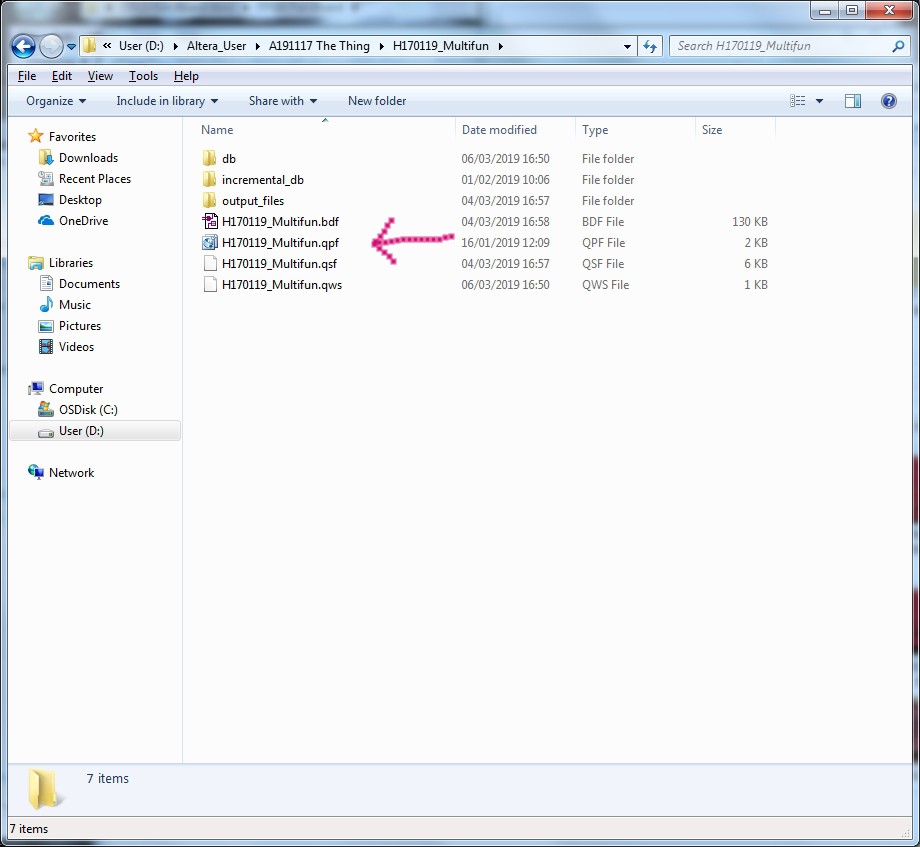
Unzip it taking its directory structure, and open it from the main Quartus II menu with "File" -> "Open Project..." selecting the file .qpf (is the extension for the Quartus II projects):
![]()
Upload the configuration into the FPGA using the JTAG connector, or with the AS connector to store it in the eeprom.
WARNING: Because this is a bidirectional interface, take in account the considerations done in the "The DEV_OE switch and led" Log.
The sketch for the MCU side (S030319_MultiFun.ino) can be downloaded from the repository.
The result is shown in this short video:
Note that the USR1-3 and BUT buttons are managed directly by the MCU (see the A191117 schematic). At the end of the video it is possible see the effect of the DEV_CLRn button (clears all the FFs inside the FPGA) and the DEV_OE switch (forces all the I/O pins of the FPGA in HiZ). The effect here is "visually" the same, but the inner behavior is different.
-
USB Blaster connection and disconnection procedure
03/04/2019 at 17:45 • 0 commentsHere are shown the connection and disconnection procedure for the USB Blaster programming device. The board in the videos is different but the procedures will apply to the JTAG and AS connectors of "The Thing" too.
USB Blaster connection procedure
After that you are ready to upload the configuration into the FPGA you must follow the suggested steps as described in the Usb Blaster User Guide:
- Check that the target (the board) is not powered;
- Connect the Usb-Blaster programmer first to the Workstation USB;
- Connect the JTAG cable to the target;
- Power the target. This means connect the board USB connector to an other USB port on the Workstation.
Remember that the USB Blaster can't power the target. The power comes from the USB connector.
Here a short video about how to connect the USB Blaster dongle:
USB Blaster disconnection procedure
Now, to disconnect the USB Blaster dongle you must follow the suggested steps as described in the Usb Blaster User Guide:
- Power off the target. This means disconnect the board USB cable;
- Disconnect the JTAG cable from the target;
- Disconnect the Usb-Blaster programmer from the Workstation USB.
Here a short video about how to disconnect the USB Blaster dongle:
-
The DEV_OE switch and led
03/04/2019 at 17:34 • 0 comments![]()
As already said in the previous Logs, the DEV_OE switch forces all the FPGA I/O pins into a HiZ state. When the DEV_OE switch is in the HiZ position, the DEV_OE led is on.
This switch comes handy in various way. A possible application is the case in which you want only use the STM32 "side" of "The Thing", and use the TEST1-2 connectors as GPIOs pins of the MCU as a "Maple Mini" clone. In this way you can simply "freeze" the FPGA holding the configuration inside.
But there is a situation in which this switch comes very very handy. Imagine that you are testing a custom interface loaded into the FPGA, and simulating this interface in a "real" situation using the STM32 as "stimulus" generator. Imagine that you have some output pins (signals from the FPGAto the STM32) and some input pins (signals from the STM32 to the FPGA).
Now what it can happen if you want change, for any reason, an input as output and an output as input in the same change?
Well, if you update the FPGA configuration at first, the new configuration will change an input as output, so this can generate a short circuit between the FPGA and the STM32 because there would be two output connected together.
So you can decide to upload the new sketch at first with the new "scenario", but in this new sketch a STM32 pin will be changed as an output, so you have two output connected together too!
The only way to break this "deadlock" is to use the DEV_OE switch to force all the FPGA I/O pins to an HiZ state and then upload the new FPGA configuration and the new sketch for the STM32 with the input/output accordingly updated. Only when both FPGA and the STM32 are updated you can safely revert the FPGA from HiZ with the DEV_OE switch again.
Remember that the DEV_OE needs to be explicitly configured in Quartus II IDE (the DEV_OE LED will turn on also if not configured!), as explained in the Log: How to configure Quartus II. Step by step guide,
-
How to configure Quartus II: step by step guide
03/04/2019 at 17:10 • 0 commentsIn the following I'll use Quartus II version 13.0SP1 (Service Pack 1) because it is last version supporting the Cyclone II FPGA series.
After installing Quartus II IDE (you can get it from here after a registration) it is necessary change some default setting on your Quartus II project to better suit "The Thing" (the default configuration is potentially dangerous for the board).
This setting must be used for every new Quartus II project.
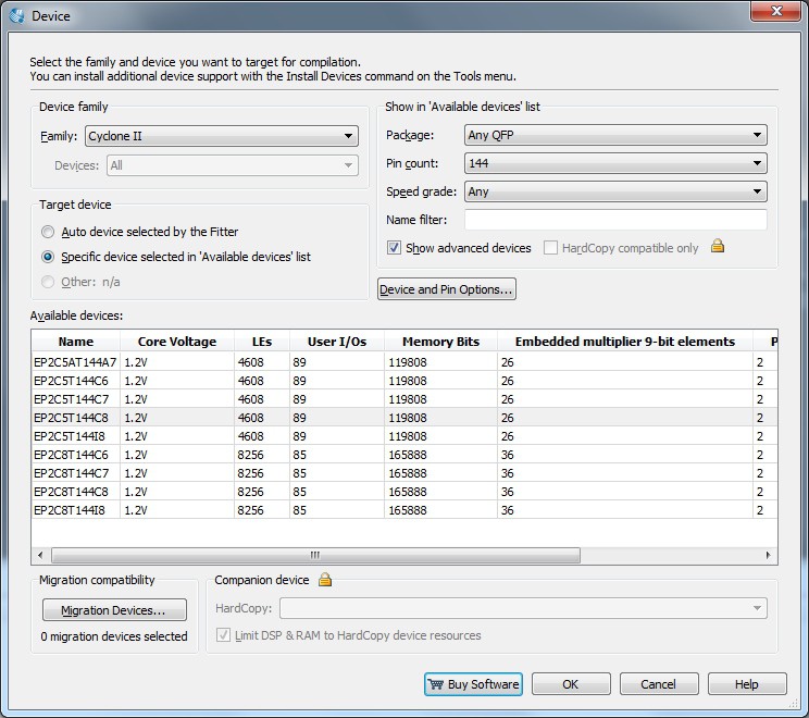
From the Quartus II menu select "Assignments" -> "Devices..."
![]()
click on the "Device and Pin Options..." button
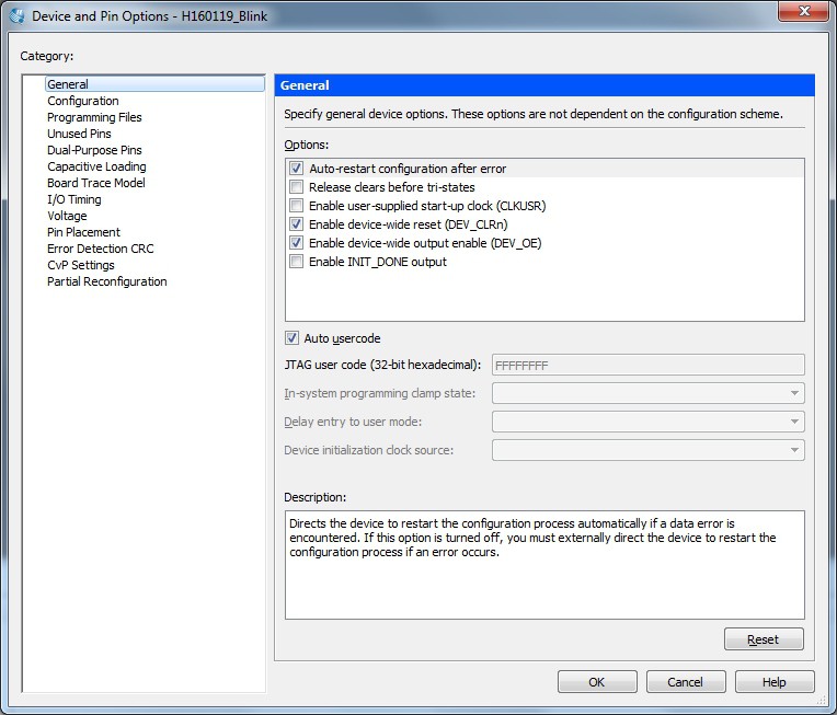
![]()
set the "Enable device-wide reset (DEV_CLRn)" and "Enable device-wide output enable (DEV_OE)" check boxes. In this way you enable the "DEV_CLRn" key and the "DEV_OE" switch in the "The Thing" board.
These are two important functions: the first will reset all the FFs inside all the LEs (Logic Elements) with the "DEV_CLRn" key, and the second will enable the possibility to set all the FPGA pins to HiZ using the "DEV_OE" switch.
Some important notes about these two function:
- The DEV_CLRn key is active also when all the FPGA pins are in HiZ;
- When all the FPGA pins are in HiZ by means of the DEV_OE switch, the "DEV_OE" led is ON;
- If you doesn't enable the "Enable device-wide reset (DEV_CLRn)" check box, the DEV_CLRn key will not operate;
- If you doesn't enable the "Enable device-wide output enable (DEV_OE)" check box, the DEV_OE switch will not operate, but the DEV_OE led will turn ON anyway. This because it is not possible from the outside to know if this function is enabled or not.
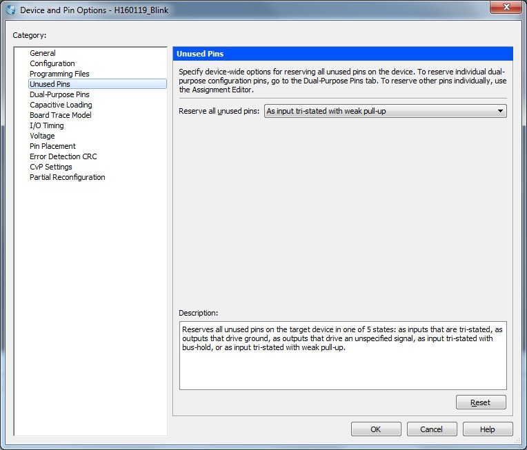
Now you will set up the state of all the unused FPGA pins. "Unused" here means not referenced explicitly in the "programming" phase.
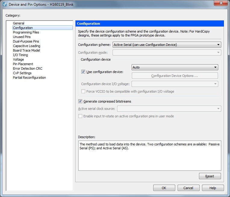
From the above windows, on the left side, choose "Configuration":
![]()
Check that the Active Serial mode is selected.
From the above windows, on the left side, choose "Unused Pins":
![]()
and in the "Reserve all unused pins" field set "As input tri-stated weak pull-up". This is the best (and safer) option for the "The Thing" board.
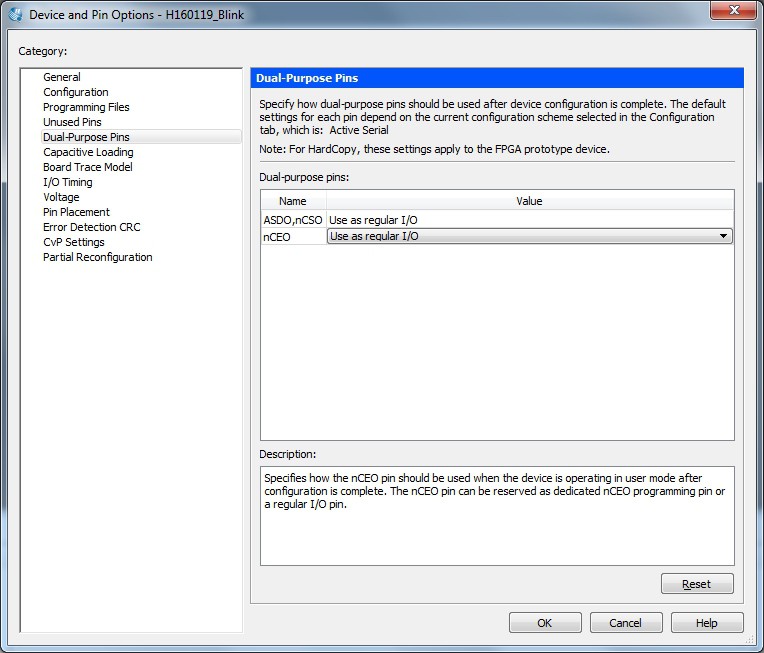
From the above windows, on the left side, choose "Dual-Purpose Pins":
![]()
and select "Use as regular I/O" for the nCEO pin.
All done!
"The Thing": FPGA + STM32
An homemade FPGA board with an Arduino STM32, "Multicomp" compatible
 Just4Fun
