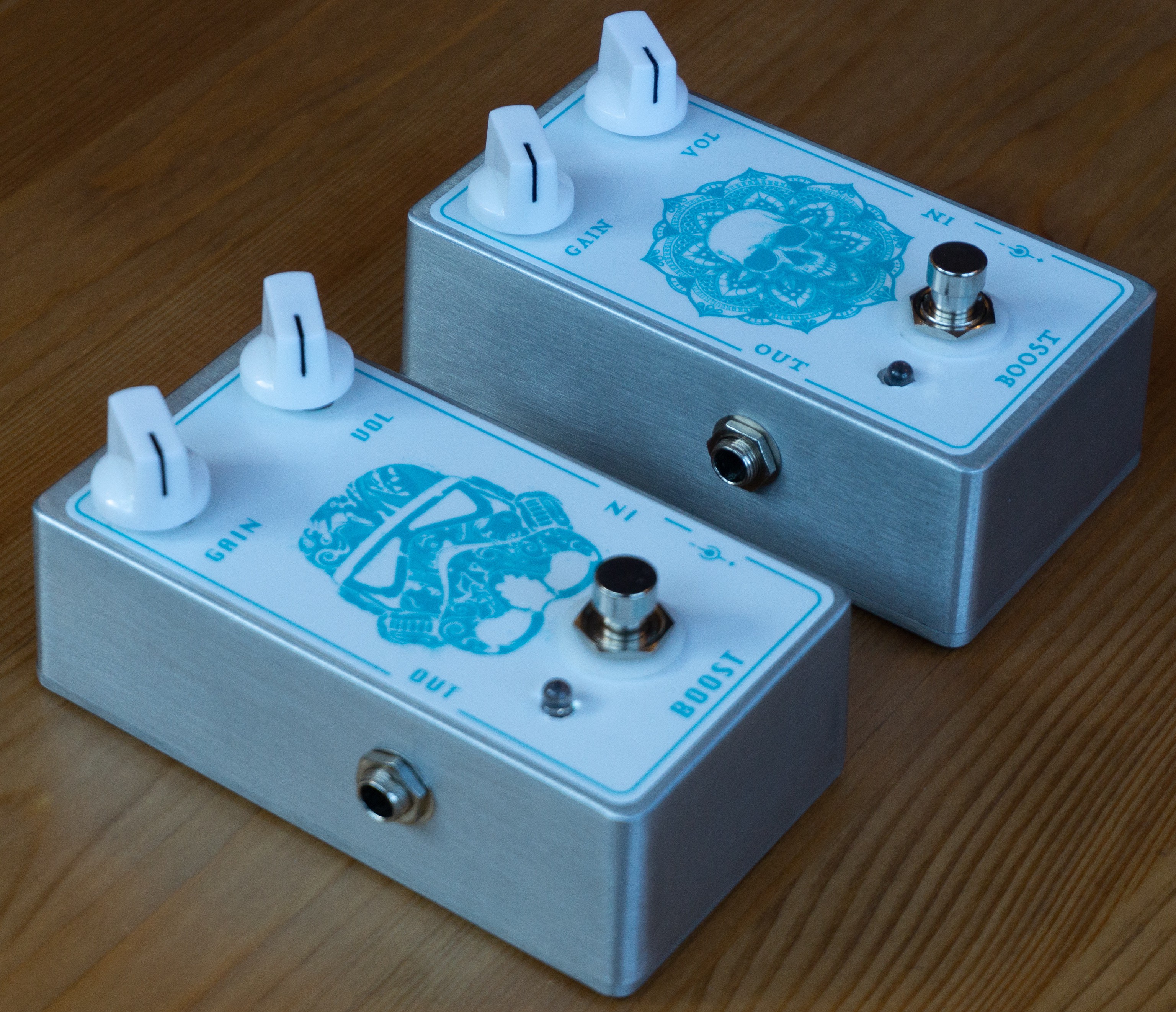
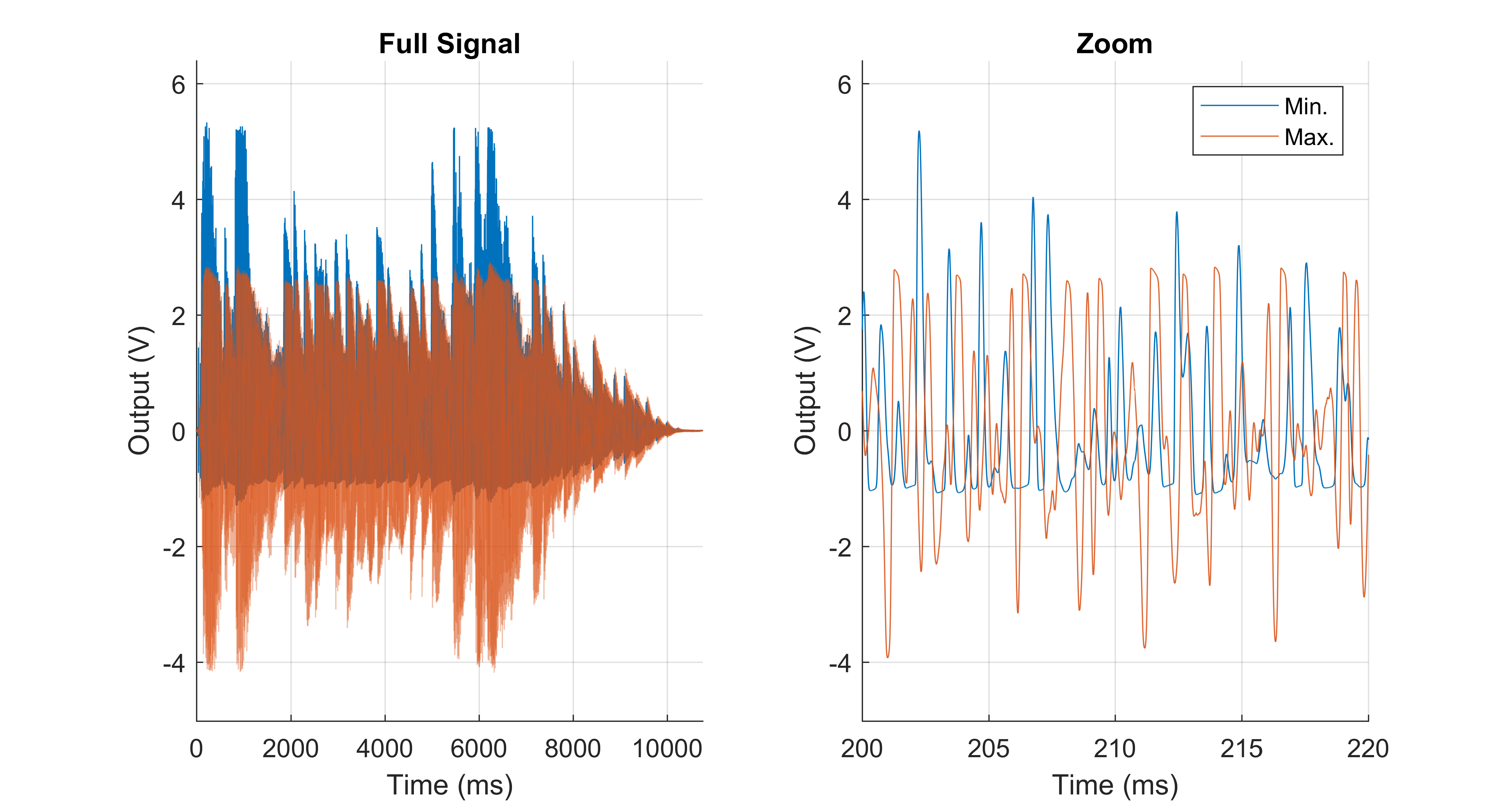
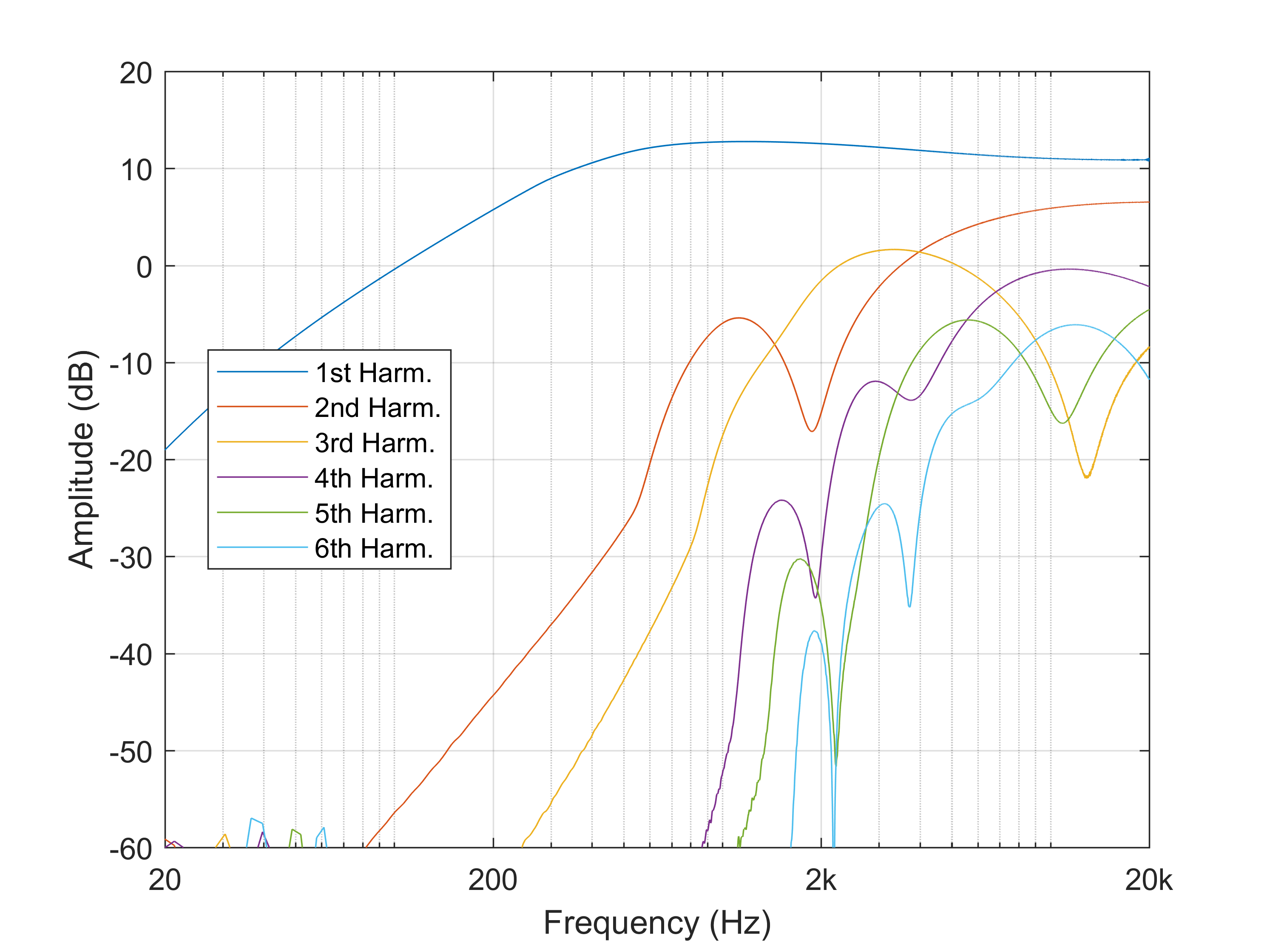
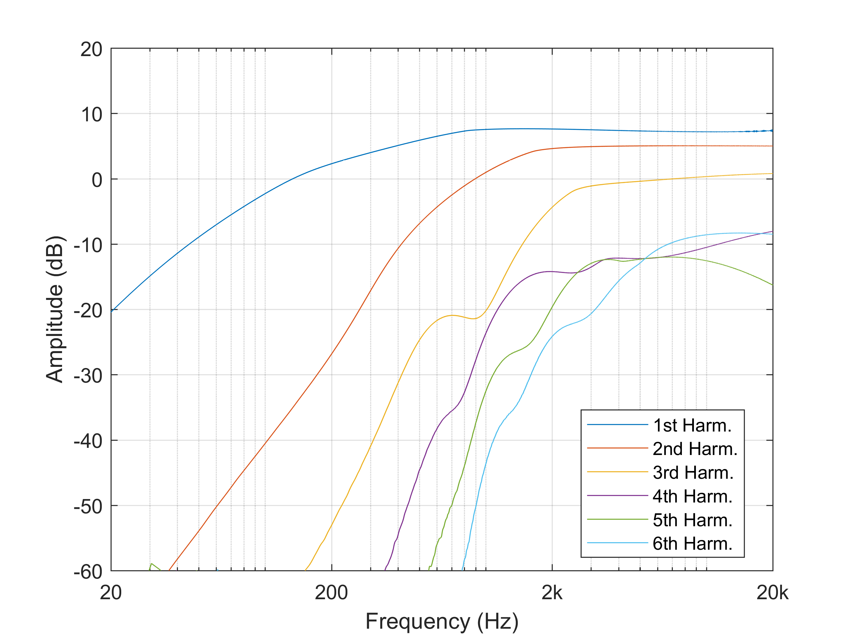
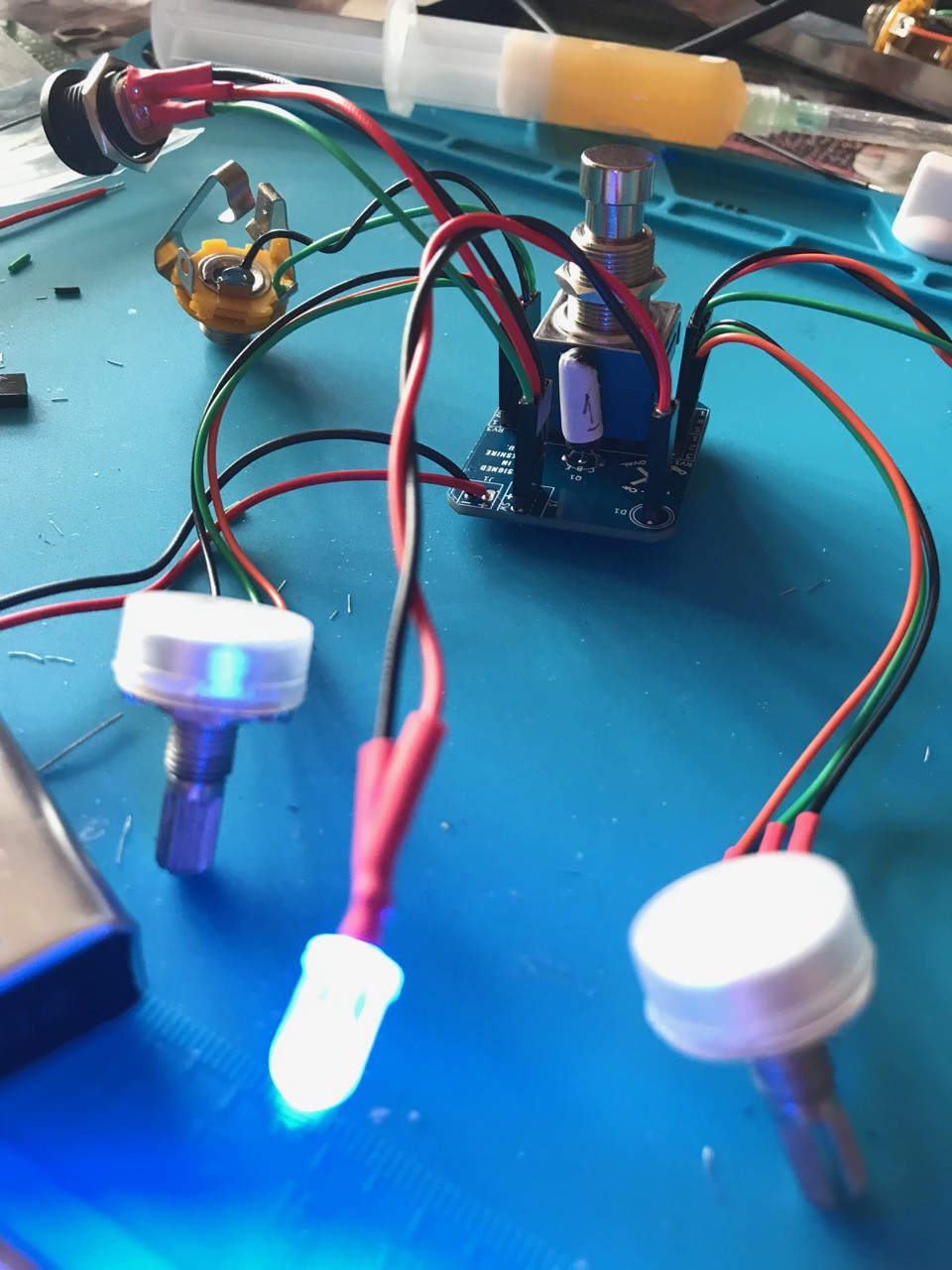
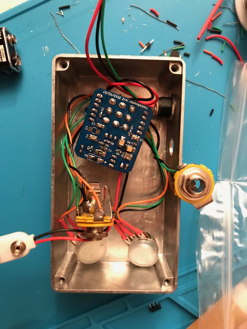
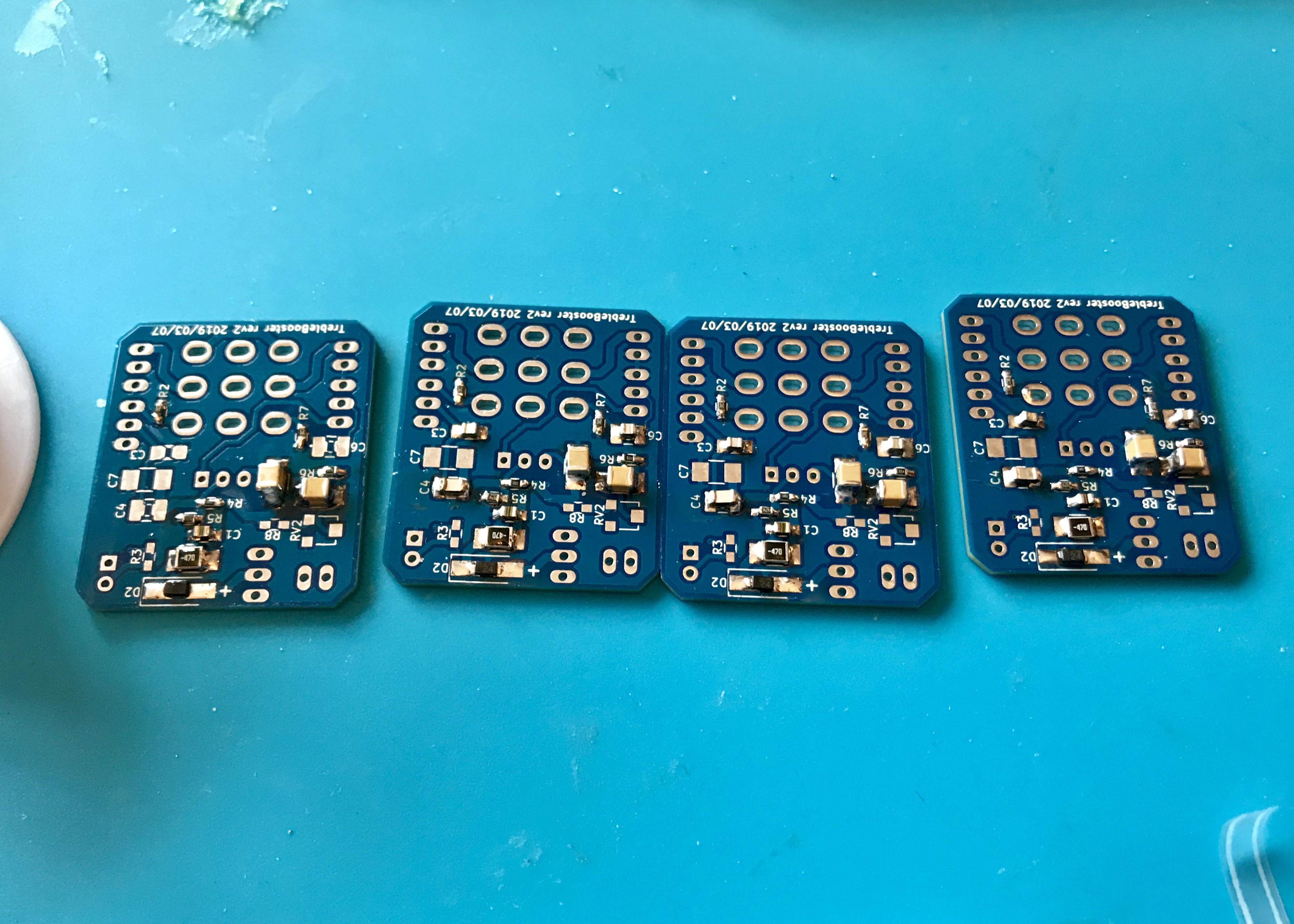
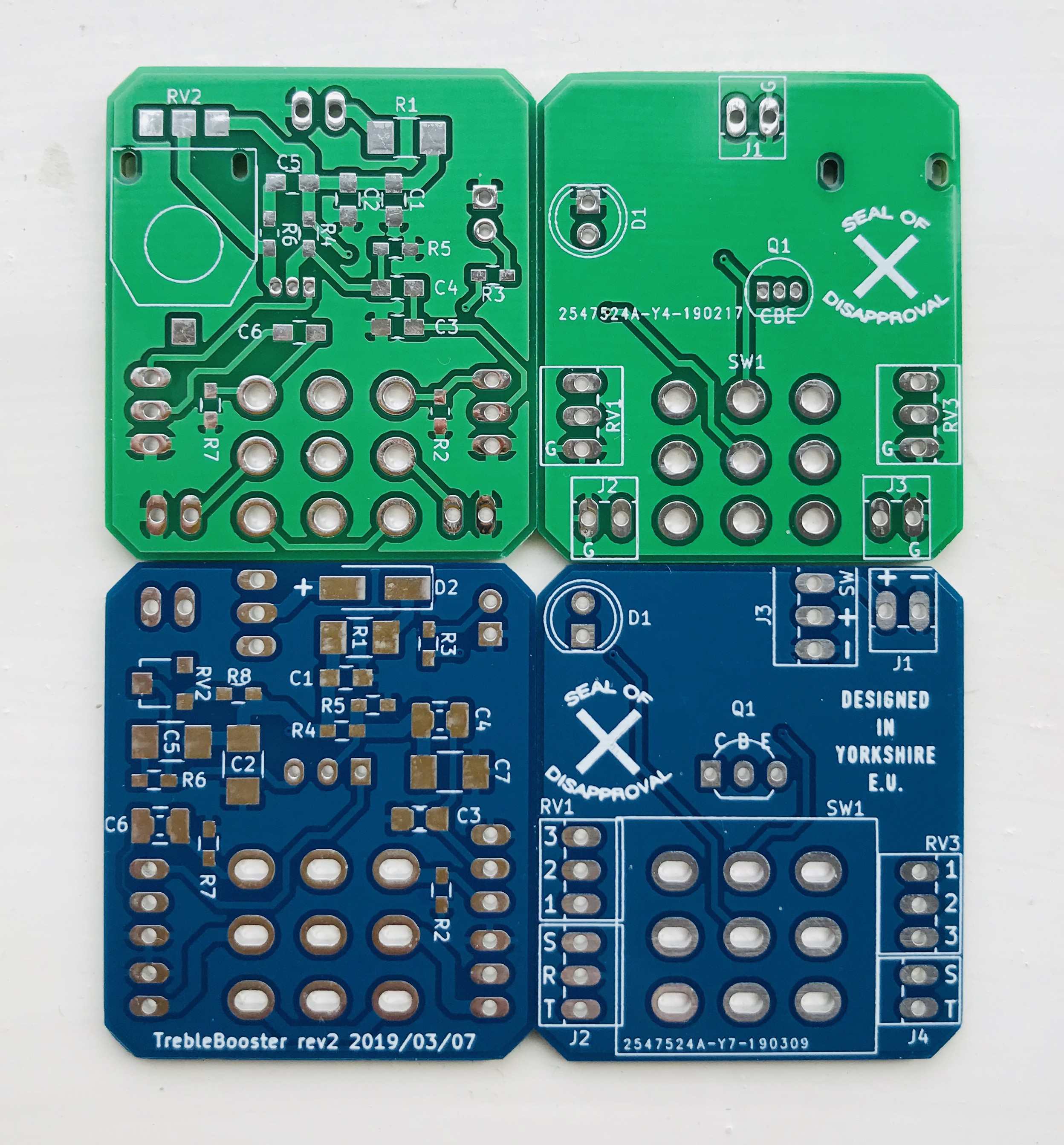
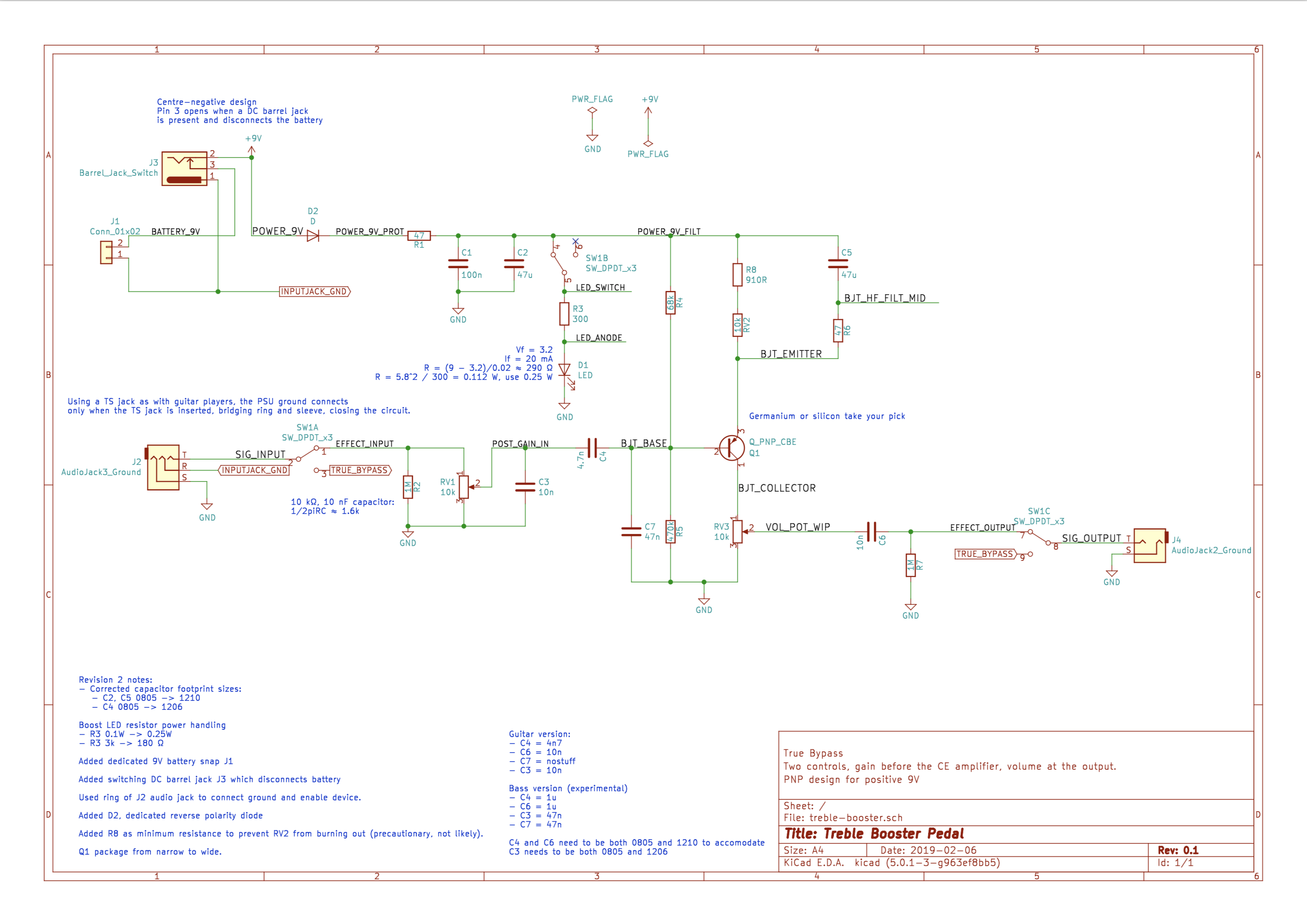
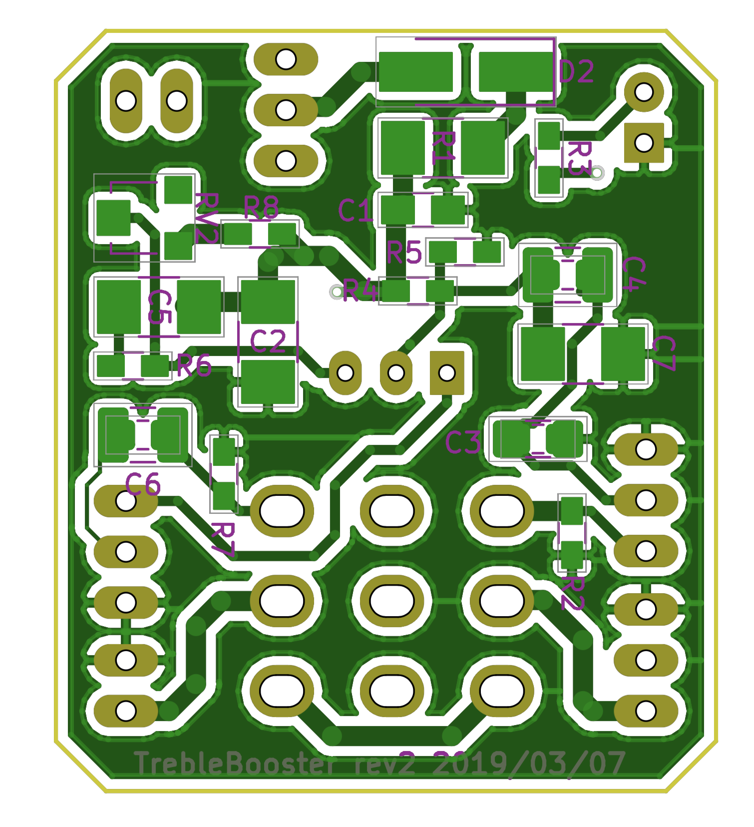
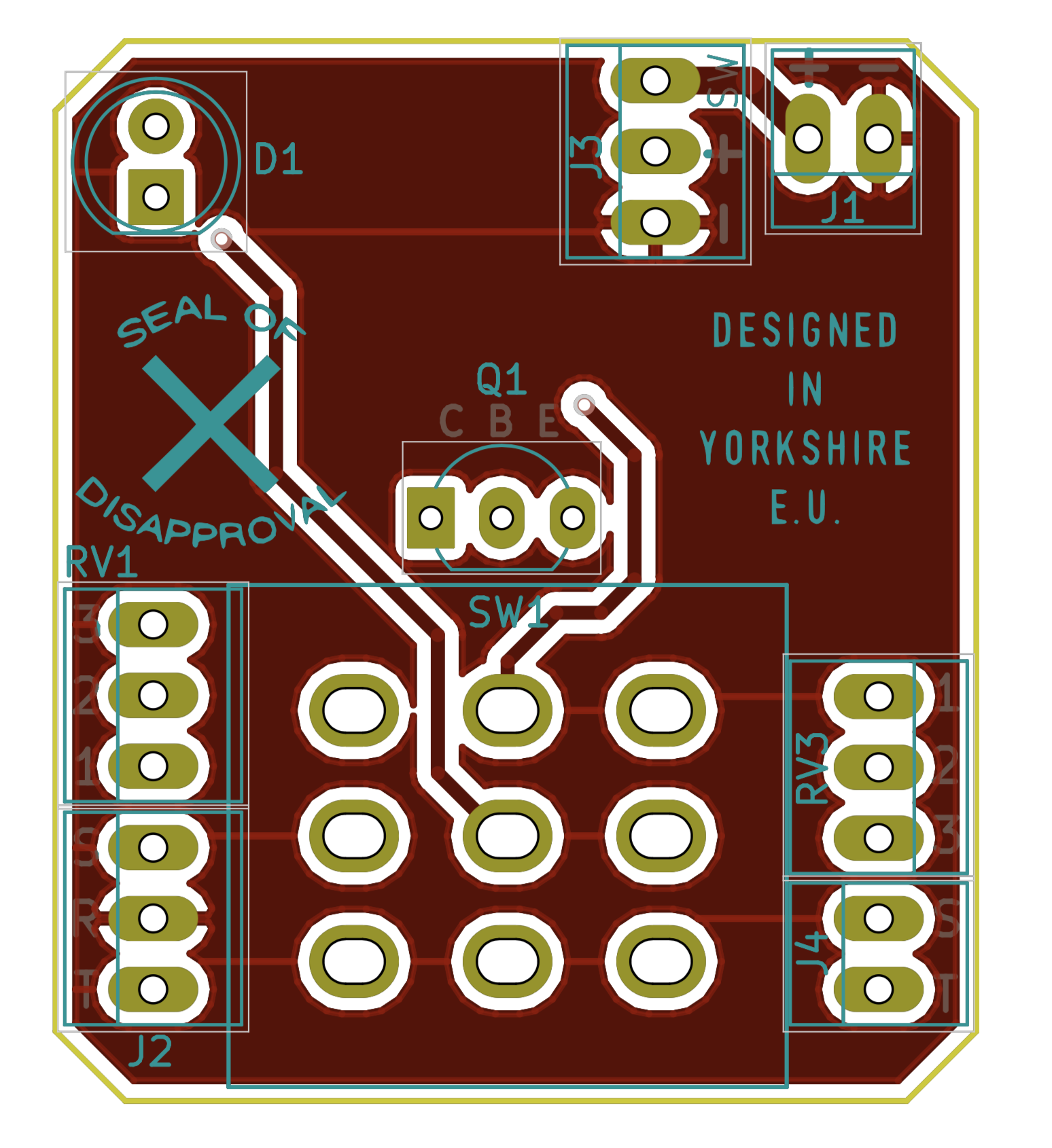
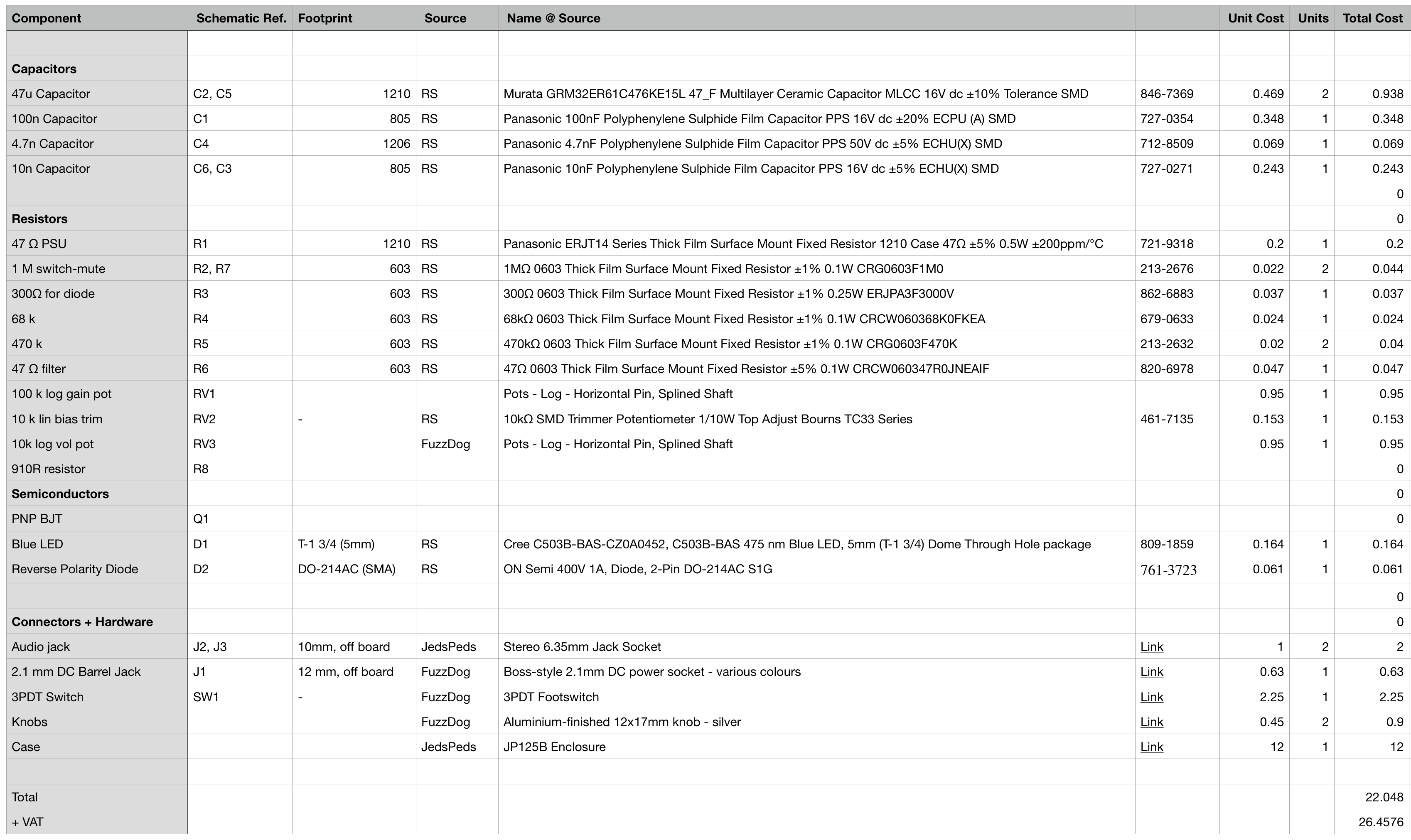
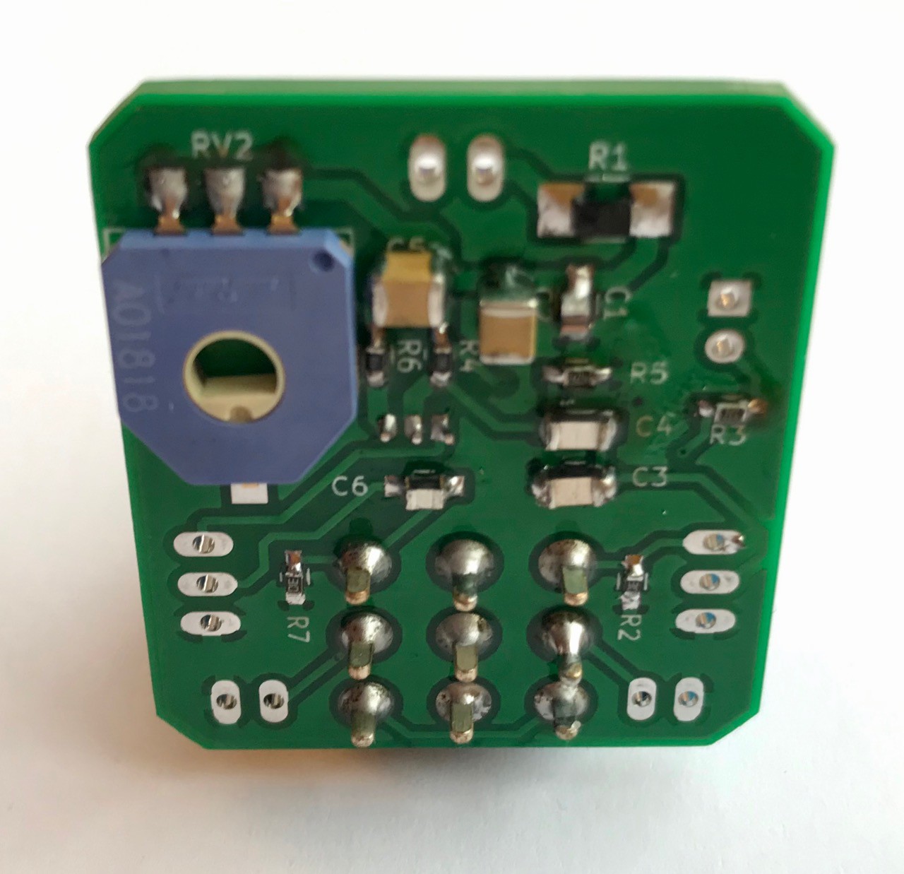
The DIY pedal community is a bit wary of using SMD (surface mount) components in a build. In this project I attempt to rectify this a bit by making a super simple treble booster pedal that utilises SMD components for everything apart from the switch and offboard connectors.
The result is a tiny PCB that is actually significantly larger than it needs to be to make it friendly to solder. The PCB attaches directly to the 3PDT typically used in a guitar pedal. The height dimensions of the components is barely larger than the legs of the 3PDT switch, so the board could be mounted in basically any case that can house a 3PDT switch.
The length and width of the current PCB is 38x32mm. This means it is a fraction too large for a Hammond 1590a, a tiny enclosure. A future revision might move the connectors to enable squeezing it into such a tiny box!
Files
custom-footprints.zip
Custom kicad footprints required for the PCB layout.
Here are the finished pedals! The decals came out great - 6 coats of spray varnish, 3 before the sticker and 3 after. I used big knobs to cover up sloppy scalpel work (below). I'll have to make a few more because they could be cool calling cards to use when applying for jobs.
I've just finished making the decals for the top of the pedals. I'm super happy with the overall design (below) but getting them on to the enclosures is going to be harder than anticipated. My printer or its ink is rubbish, leaving patterns across the design that look crap.
I would put the original documents for the decals on hackaday but since they use copyright material that wouldn't be right. I'm using the artwork for 1 off, personal designs so I hope that's covered under fair use.
Also for the next iteration I'll need to mark the drill holes and get better at cutting the material. One step closer though.
Getting the PCB mounted in the case required desoldering the header pins for the input and output jacks, as well as the LED. It fits snuggly now, but I also have a reference design for the future so I know which way to solder the pots without trial and error. The only necessary socketed offboard connector is the DC jack as hardwiring it would prevent the PCB from coming free of the case.
Testing, 1 2 3...
From initial tests the circuit works fully. When the effect is bypassed there is no obvious change in signal (true bypass is great). When the effect is engaged it distorts plenty. The volume pot was wired backwards but with the socketed pins it only took a minute to fix.
The first proper test I ran on the circuit was around the biasing trim-pot, RV2. This ought to change the DC gain of the amplifier and effect the frequency response somewhat too.
The below image shows a the output of the pedal when driven with a guitar signal. The blue is when the bias is set to minimum, and the red when set to maximum (or it might be the other way around, orientation is confusing when I haven't marked the PCB).
A huge change in bias can be observed, but I don't really know what this sounds like. When setting up a pedal for the beta testers I'll get them to play it while I calibrate the trim pot to see what tone they like best, and use this to work from.
Swept-sine technique
To gain some intuition about this I wanted to try a swept-sine characterisation, which basically provides an amplitude response at each harmonic of a signal, providing insight into the distortion behaviour. Results can be seen below:
Here's a quick breakdown for the figure. It is an amplitude response, like that which you'd use to show the gain of different frequencies for a linear circuit. Most will be familiar with this concept if you've studied signals and systems. Instead of just the first harmonic (in blue), which is what you'd get with the typical amplitude response, this provides the response for the harmonics caused by the nonlinear behaviour of the signal. One gotcha of the process is that the higher harmonics will look more and more bandpassed as this is a limitation of the method - you need longer signals and FFTs to provide a wider pass-band range.
My basic interpretation of the plot is that the treble booster cuts the bass and boosts the treble, and there's a lot of distortion too. This data was gathered at maximum bias and full gain.
The test can be repeated for minimum bias:
The response is clearly quite different, and again I don't know which sound will be preferred. What's cool about this representation is that once I've found "that" sound which users love, I can characterise it and calibrate the following pedals to match it. Sure you could do it by ear but why not get some data behind it.
This revision I decided to try PCB headers to modularise the design. Particularly with the DC barrel jack, it would be much easier to mount the connectors with header pins but they just don't fit the case:
The last build I soldered the pots the wrong way around, so I'll have to think carefully about which headers to remove to keep flexibility, but also to fit it in the darn case. The audio jacks are easy to get right, as is the diode. The potentiometers and the DC barrel jack will probably stay on headers.
They’re a work in progress! These boards include a bunch of new features:
- The pedal is only enabled when an input jack is present
- A dedicated header is present for the battery.
- BOM changes reduce the cost of the biasing resistor and switch, while improving the amount of space available for layout.
- There’s an experimental bass version which I want to try out! Dual pads allow a variety of component stuffings.
Here is a comparison between first and second revisions:
The new blue boards look great, but cost an extra $8 to manufacture. I learned a wise lesson once to make each revision visually different so that you don’t end up with a box full of the same stuff!
Admittedly, I love OSHpark and the PCBs they make and have used them enough to have 3 stickers on my laptop from them. But currently I'm poor as anything and have found that all of my designs are only $2 on JLCPCB at the moment.
One of the great things about JLCPCB is that it gives you live updates of how your boards are doing. Currently these have copper on but nothing else. Looking forward to getting them back!
I've posted this project on reddit asking for a review of the schematic and layout, but the images seem to be dodgy imgur, so I'm posting them here too. Also available on imgur: https://imgur.com/a/UPDZnNs
Schematic
Schematic notes
The circuit is left completely open unless a TS jack is present at J2, which then makes the ground connection between INPUTJACK_GND and actual ground. This is to prevent wasting power.
J3 is a switching barrel jack that disconnects the battery when a 9v jack is present. There's no overvoltage protection for now, but D2 prevents reverse polarity. The voltage drop of D2 (0.7V) is fine because the desired goal is distortion anyway.
The main version of the schematic is for guitars, but I want to make one for a bass playing friend for which I've noted alternate stuffing options. These result in odd footprints where I'm placing both 0805 and 1210 or 1206 to fit bigger capacitors and let more bass through. It's not really a treble boost pedal anymore when I do that! But it's only experimental.
The pedal is true bypass which means there are no components in the signal chain when the effect is disabled. To prevent the switching artefacts from being too bad R2 and R7 pull down the DC blocking caps.
PCB layout, bottom
Bottom copper, solder mask, and silkscreen notes Copper pour is GND.
C3, C6, and C4 all have dual footprints to enable different stuffing options for bass and guitar. The actual ground return will run out of the ground pad next to the R2 indicator, up to the input jack connector and back to the board.
The only real custom footprint on here is SW1, the large 9 pads in the middle. I designed this from measurements of a 3PDT footswitch that the board will be soldered to directly. This might not be ideal from a vibrations perspective...
All other hardware is offboard and will be mounted in the enclosure itself.
PCB layout, top
Top copper, solder mask, and silk screen notes
Copper pour is INPUTJACK_GND, trying to make both GND and INPUTJACK_GND super low impedance and with good connection through the offboard jack.
Typical edgelord silk screen items to make the PCB seem cool. Ignore political opinions.
BOM
BOM notes
There is a different stuffing for the bass version as noted, but I didn't thing it would be necessary to add here.
Some elements are missing complete information which I will rectify, but again probably not necessary for a review.
The finished PCBs have arrived from JLCPCB who did a good job of the board, cheaply and promptly.
Here is a list of total fuck-ups on the rev1 board: - I did not update footprints after adapting the BOM, meaning some caps were waaay too big for their associated footprint. I still soldered them on though! - The center hole of the trim pot (RV2) should have been drilled but I didn't realise... The fourth pin on the opposite side is only for support so I can still solder the three functional pins but it is not flush. - The BJT pins are a bit close to each other, and could do with being moved further apart. - There is a typical guitar pedal layout where the power source is only connected if there is an input jack plugged in. I left this out entirely but would be great to have in rev2. - If I make the switch holes bigger I could fit much cheaper 3PDT switches instead of the one I ordered off RS which cost over £4! - I should add another footprint for a power supply filter resistor as I hijacked R1 for a reverse polarity protection diode.
Everything fit on the board, but you can definitely tell where there is 1210 on a 0603 pad.
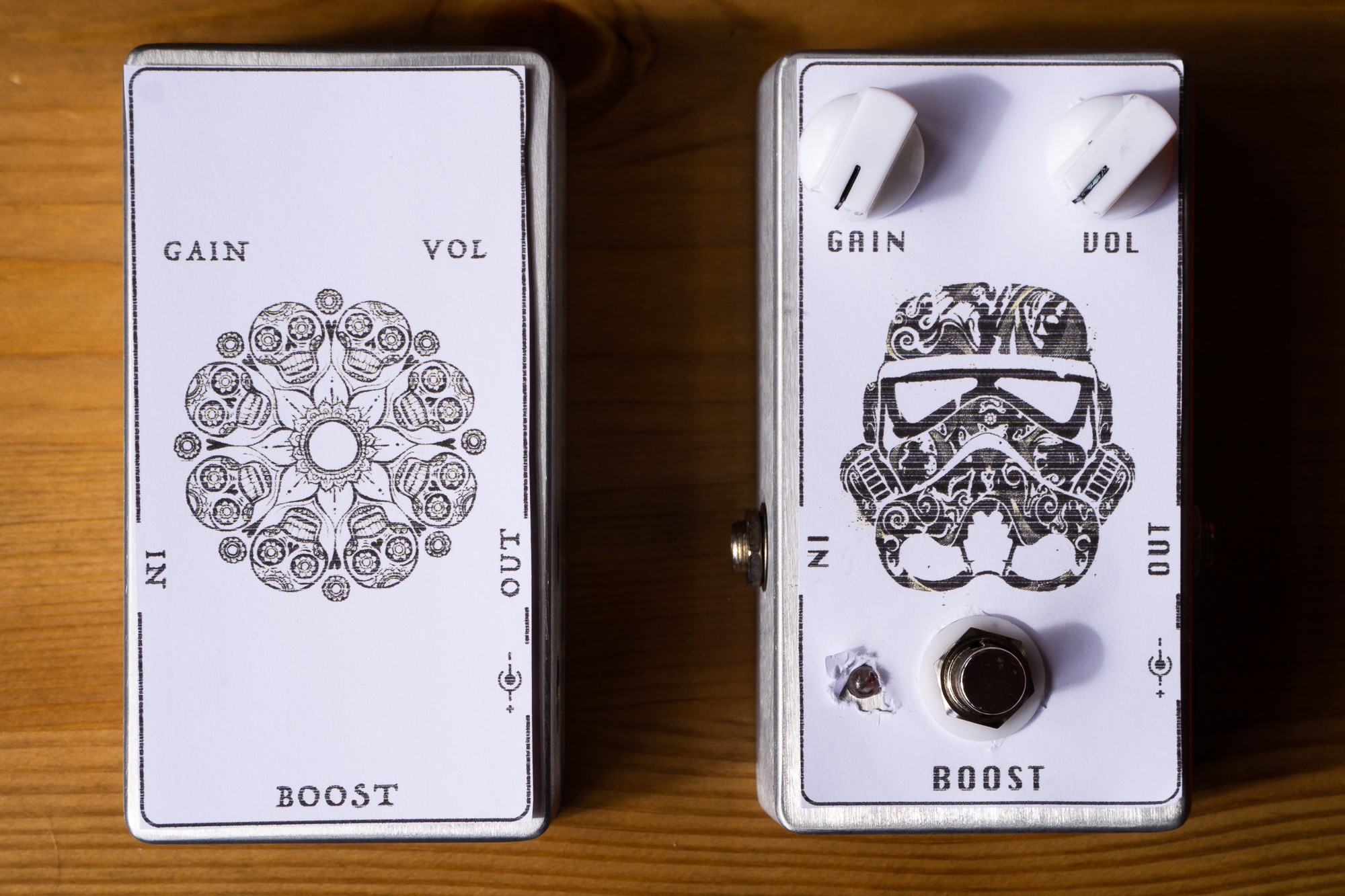
Is that going to be the actual pedal case design :)