 Jack Flynn
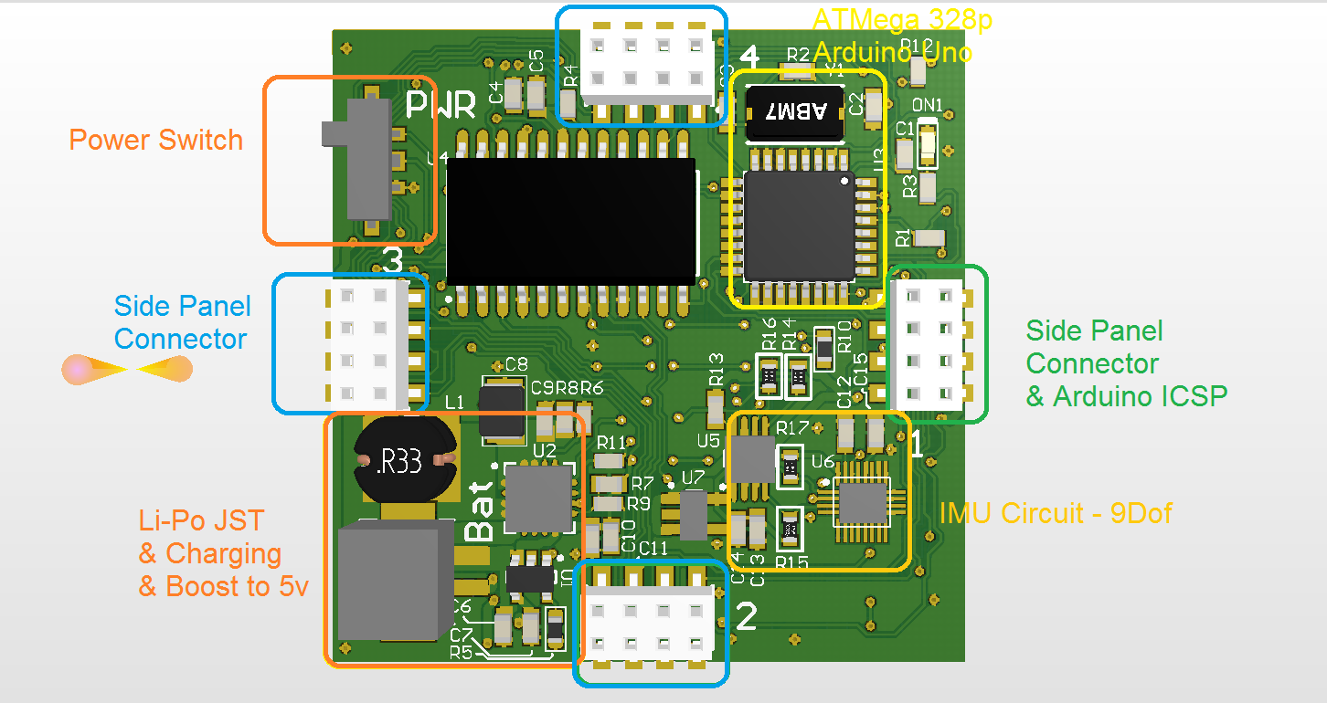
For the initial design of the Bottom PCB I restricted myself to a 2 layer PCB. It's quick and dirty and really it should be a 4 layer so that I can offload power and ground to the internal layers. However, for an initial design and prototype I think it'll work. The Bottom PCB is the "Brains" of the project. It has the following features;
Arduino compatible ATMega328P
4 x Panel Connectors for the side panels - 1 of these can be used with an ICSP programmer to burn the Arduino Bootloader to the ATMega328P.
IMU - LSM9DS1TR - for orientation tracking i2c accelerometer, gyroscopes and magnetometer
LiPo JST Battery connector with charging chip and 5v Boost - based on Adafruit 500 Powerboost
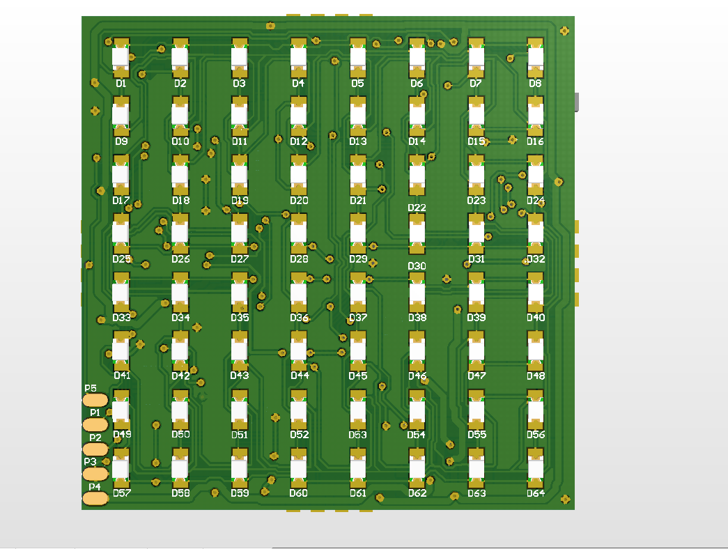
Max 7219 LED Driver for 64 LEDs. Communication via an SPI-similar bus.
And on the back side we have the 64 SMD 0805 LEDs and exposed pads for pogo pins to allow for charging and reprogramming.
Discussions
Become a Hackaday.io Member
Create an account to leave a comment. Already have an account? Log In.
Clever; reusing one of the headers for ISP programming.
Are you sure? yes | no
Thanks! Not going to lie, that was one of my favourite little design quirks that feels super useful
Are you sure? yes | no