 Alastair Hewitt
This is by far the most complex board I've ever worked on and I assumed it would take the rest of this month to lay out. However, things are progressing a lot faster than thought and it's possible a Rev. 1 board could be ready for fab by the end of the weekend.
This may be wildly optimistic though... The last 10% of the traces could take 90% of the time to manually route. It's possible the last few traces may not be routable at this density and the entire layout could get scrapped when it's 99% done.
Discussions
Become a Hackaday.io Member
Create an account to leave a comment. Already have an account? Log In.
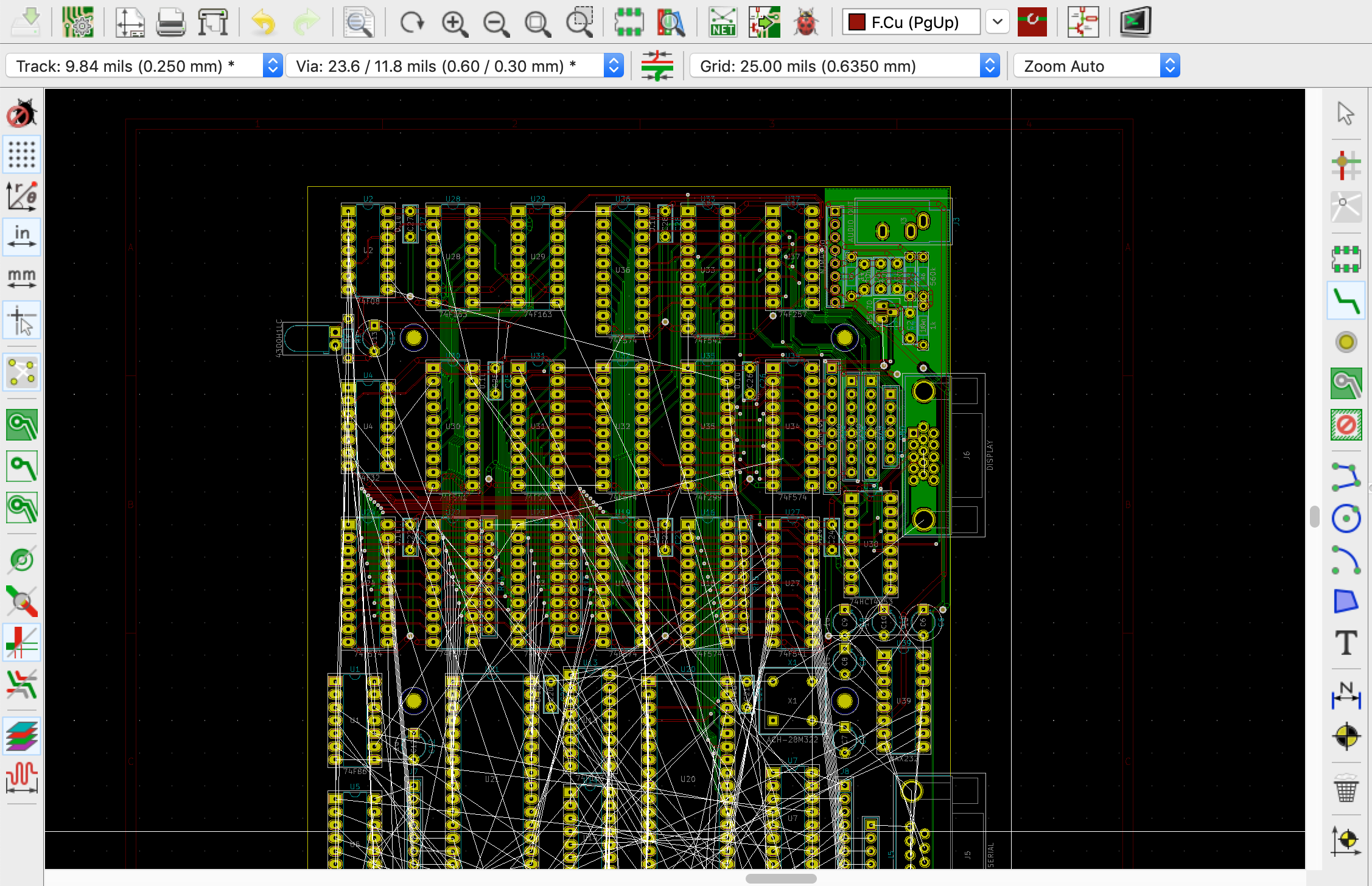
Kicad doesn't have an autorouter built in, but you can use it with FreeRouting. I tried that early on and it was useless. I spent many weeks placing the components before starting the actual routing this week. There's a lot of different busses, so you have to work with a lot of tradeoffs at this density.
I've spent about 24 hours hand routing and got to about 90%. I thought I could do it with single traces between pads and used 10 mil traces with 8 mil clearance. It now looks like I can't complete the routing with the current rules and I've decided to start over with 8 mil traces and 7 mil clearance. This is just small enough to get two traces between the DIP pads.
Are you sure? yes | no
24 hours hand routing is quite fast for such complexity...
You could also change design rules but leave existing traces as they are... but that is perhaps not pleasing to the eye.
Are you sure? yes | no
Are you routing by hand, or do you also use an autorouter ?
You can set the designrules such that two traces can pass between two 0.1" spaced DIP pins. This gives much more routing options. For my Kobold pcb I use 6 mil traces for this, that is OK for most Chinese board houses.
And it also pays off to spend extra time to find a good placement.
Are you sure? yes | no