Alastair Hewitt
-
Routed
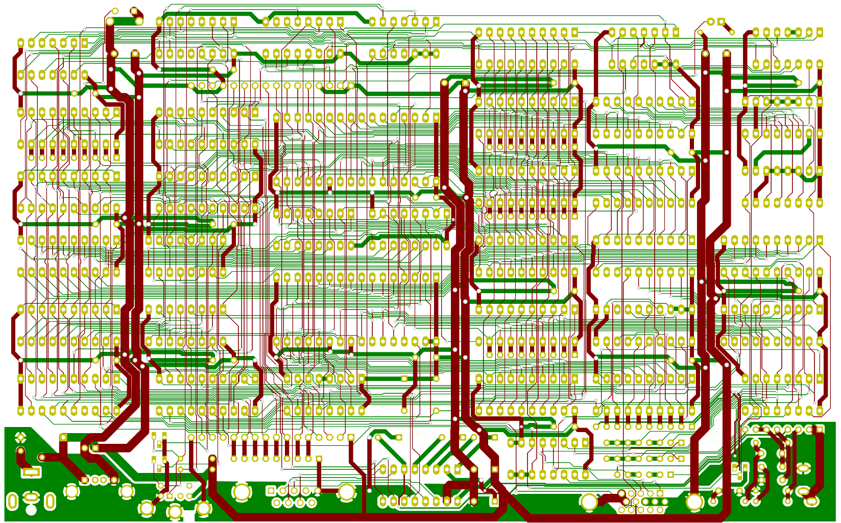
11/11/2019 at 01:13 • 5 commentsHot off the press... Routing was just completed using 8 mil traces with 7 mil spacing. This was 100% hand routed and took about 30 hours. The original attempt using 10 mil traces with 8 mil spacing failed after about 24 hours of work.
The ability to route two traces between the DIP pads was the only way to complete routing at this density (40 chips on 8" x 5" double-sided board). Extra space was also added around the ROM to allow a ZIF socket to be installed.
![]()
Update: DRC checks pass and initial visual inspection done. The power barrel jack needs fixing and possible additional mods after further review. If everything checks then it will get shipped for fabrication tomorrow.
-
PCB Taking Shape
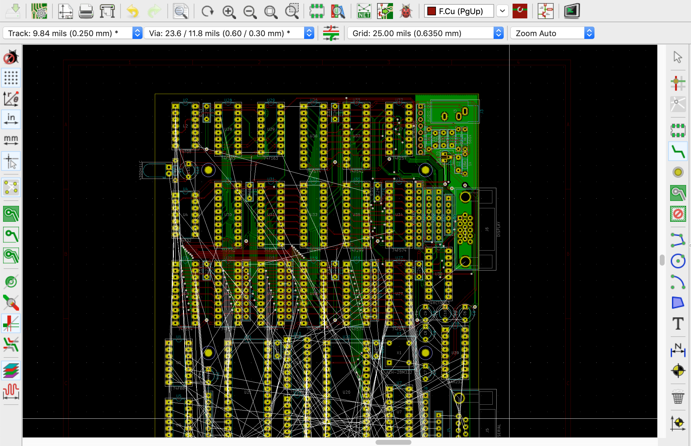
11/07/2019 at 15:58 • 3 commentsThis is by far the most complex board I've ever worked on and I assumed it would take the rest of this month to lay out. However, things are progressing a lot faster than thought and it's possible a Rev. 1 board could be ready for fab by the end of the weekend.
![]()
This may be wildly optimistic though... The last 10% of the traces could take 90% of the time to manually route. It's possible the last few traces may not be routable at this density and the entire layout could get scrapped when it's 99% done.
-
Long Road Ahead
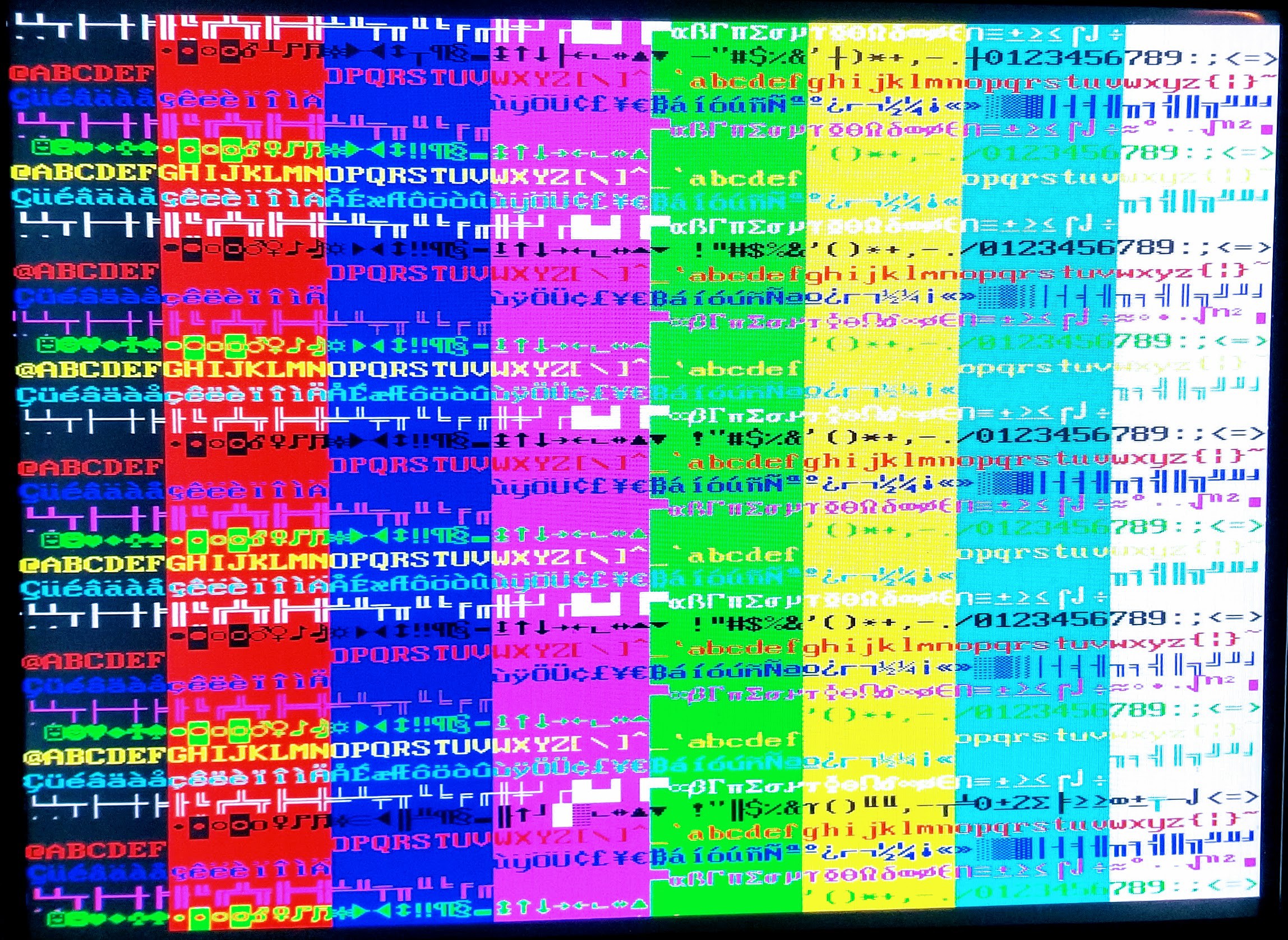
11/04/2019 at 02:40 • 2 commentsThis was a long fought victory. Two pairs of loops were added, the first to fill the video memory with 64 columns of text repeating every 4 lines with the enumeration of code page 437. The second repeats the background colors as 8 columns and foreground colors and fonts on alternating rows.
![]()
There were various issues getting this working. One was a bug in the build script that generates the list of valid instructions. Most of the other issues related to stability. The supply voltage sags from one side of the breadboard to the other. The difference is over 0.3V, but the most stable range of operation falls within a narrow 0.1-0.2V range. Adjusting the supply to stabilize one side will destabilize the other. It also appears the NOR flash is aging each time new code is flashed. The access time is slowly increasing and the once stable 25MHz is now glitching (spot the glitch in the last sequence of 0-9 above).
There are a few more tests to run, but the value of developing and testing on the breadboard is rapidly diminishing. The PCB is starting to progress with a final component layout and routing strategy. The first revision will be a simple two-sided board to test the layout and power distribution. Further revisions will likely switch to 4-layers depending on actual stability.
-
90 Column Text
10/31/2019 at 01:26 • 1 commentThe scaler appears to be the most forgiving of the video devices on hand and a video signal was just possible with a clock of 29.4912MHz. This is a nice UART frequency but it is probably out of reach even when the circuit is on a real PCB. There is one frequency available that may be attainable and that is the other VGA clock: 28.322MHz.
The standard 25.175MHz VGA clock generates a horizontal resolution of 640 pixels, or 80 columns of 8-pixel wide glyphs. The 28.322MHz frequency is 9/8ths as fast and generates a horizontal resolution of 720 pixels, or 80 columns of 9-pixel wide glyphs. Of course, this is with the VGA horizontal frequency of 31.5kHz, where this design requires 38.4kHz.
The line length is shortened in order to get to the 38.4kHz. In this case the effective horizontal resolution would be reduced to 575 pixels, or around 71 columns of text. However, this shorter line is only required to support serial communications. This would be a requirement for something like a text based web browser, but non-network applications can use the original VGA timing. This would result a text mode with 90 columns using the font ROM's 8-pixel glyphs.
This change requires two different timing loops. The 38.4kHz loop would divide the line by 184 process cycles and the 31.5kHz loop would divide by 225. The decision had already been made to handle either serial or audio, but not both concurrently. It now makes sense to split these features between these two video modes. The additional 41 process cycles in the 31.5kHz loop can then be used to process the audio. The rest of the loop would operate the same interpreter fetch and execute cycles as the shorter 38.4kHz loop. Therefore the only change between the loops would be a longer H-sync cycle to process the audio.
There would still be text and graphics modes with both loops and they can both support two video modes each depending on the field rate. The following examples show the supported video modes:
31.5kHz Horizontal, 60Hz Field (native 720x480 60Hz VGA)
- Hi-res Text: 90x60
- Lo-res Text: 90x30
- Hi-res Graphics: 360x240
- Lo-res Graphics: 180x120
31.5kHz Horizontal, 70Hz Field (native 720x400 70Hz VGA)
- Hi-res Text: 90x50
- Lo-res Text: 90x25
- Hi-res Graphics: 360x200
- Lo-res Graphics: 180x100
38.4kHz Horizontal Scan, 60Hz Field (**native 800x600 60Hz SVGA)
- Hi-res Text: 70x75
- Lo-res Text: 70x35
- Hi-res Graphics: 280x200
- Lo-res Graphics: 140x100
38.4kHz Horizontal Scan, 75Hz Field (**native 640x480 75Hz VGA)
- Hi-res Text: 70x60
- Lo-res Text: 70x30
- Hi-res Graphics: 280x240
- Lo-res Graphics: 140x120
** 38.4kHz modes are slightly modified versions of the VESA standards
-
80 Column Text
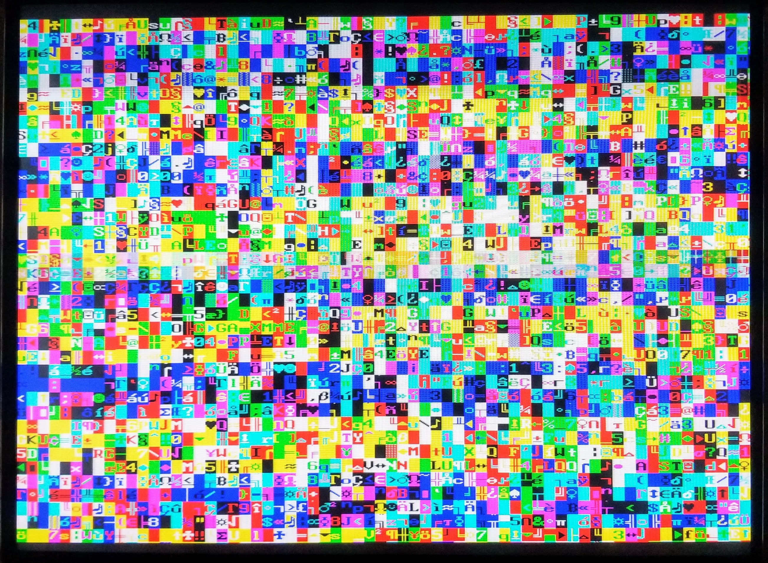
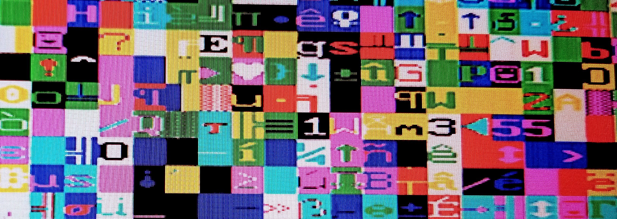
10/29/2019 at 00:10 • 2 commentsThe testing phase has been using NOR flash memory. The fastest version is rated at 70ns, and although much better performance was observed, it will not support a dot clock above 25MHz. The final design will use the 55ns rated Atmel AT27C020. A similar performance boost was assumed and this suggests a clock of 32MHz might be possible with this faster memory.
The AT27C020 is a one-time programable (OTP) device and it was finally time to commit a device to the video timing code. The 32MHz version of the code was programmed and tested. Unfortunately, the OTP ROM did not support 32MHz, or at least, not on the breadboard. The highest frequency achieved (with the crystals on hand) was 27MHz.
This clock was just fast enough to meet the 50Hz limit on the CRT and display what the faster clock would show at 60Hz. The result below is the high-res text mode of 80x75. There is no horizontal blanking, so the random text actually wraps around to display about 87 columns of text. Click on the image and zoom in to see it in all its glory!
![]()
I believe this might be the highest density text ever produced by a TTL-only computer.
-
GPU Build Complete
10/27/2019 at 23:06 • 0 commentsThe last few chips were added this weekend to complete the GPU functionality. The system had been stabilized to work with the 32 MHz dot clock and the initial testing started with that. Unfortunately things didn't work at all once the font ROM was engaged!
Up until now the GPU has been kept in its blanking state for CPU testing. This is where the GPU addresses the RAM location 0x1FFFF, which returns the same byte on every GPU cycle. This means the ROM data bus alternates between the CPU code/ALU result, and a single value. This all changed once the GPU was brought out of the blanking state. Now there is the full entropy on the bus with alternating code/ALU and glyph data. This creates a much more complex set of signals and the already noisy bus became too unstable to latch valid data.
Another issue is the memory speed. The 32 MHz dot clock requires memory access time of better than 50ns. The NOR flash was measured at around 35ns in the blanking state, but couldn't keep up when the font lookup was also being processed. Reducing the clock to 25 MHz brought things back under control, but only just. There is still a lot of glitching mainly caused by noise from the following rat's nest...
![]()
The video loop described in the previous log was updated for the slower clock to produce 65 columns by 38 lines of text. The video memory is not initialized, so the color and text data is just random. The following photo shows this data when displayed on the CRT:
![]()
The CRT works great and the video signal is crisp and well defined. This is unlikely to the typical display method, so the signal was also examined on an LCD. This is where things start to get interesting though. The 38.4kHz/60Hz video signal is treated as SVGA and assumed to come from a 40MHz dot clock. This means the LCD will oversample the signal and record all the timing glitches when one color changes to another.
This effect can be seen in the following detail from the LCD:
![]()
This ghosting was anticipated and the RGB bits were passed through a final set of flip flops to make sure all the bits change simultaneously. However, this did not solve the problem since the logic level rise and fall times differ. The final stage of flip flops made very little difference to the quality of the signal. In fact the version with the flip flops displayed additional noise caused by crosstalk with the other flip flops on the chip.
Below is the same section of color text. The version at the top was resampled by the flip-flops, while the version on the bottom is the raw output direct from the 2:1 multiplexer.
![]()
![]()
These observations have been taken in to consideration for one final update of the schematic. Everything except the audio and serial communications has now been verified. It is getting harder to test though and full speed testing will not be possible with the breadboard. The plan is to now proceed with the PCB layout and then continue testing when the rev 1 board is available.
-
Video Timing
10/21/2019 at 04:20 • 0 commentsThe first 5 chips of the GPU were added this weekend. This included the H register (4-bit counters and buffer) and the V and S registers (8-bit flip-flops). Most of the time was taken up with software development for a video timing loop.
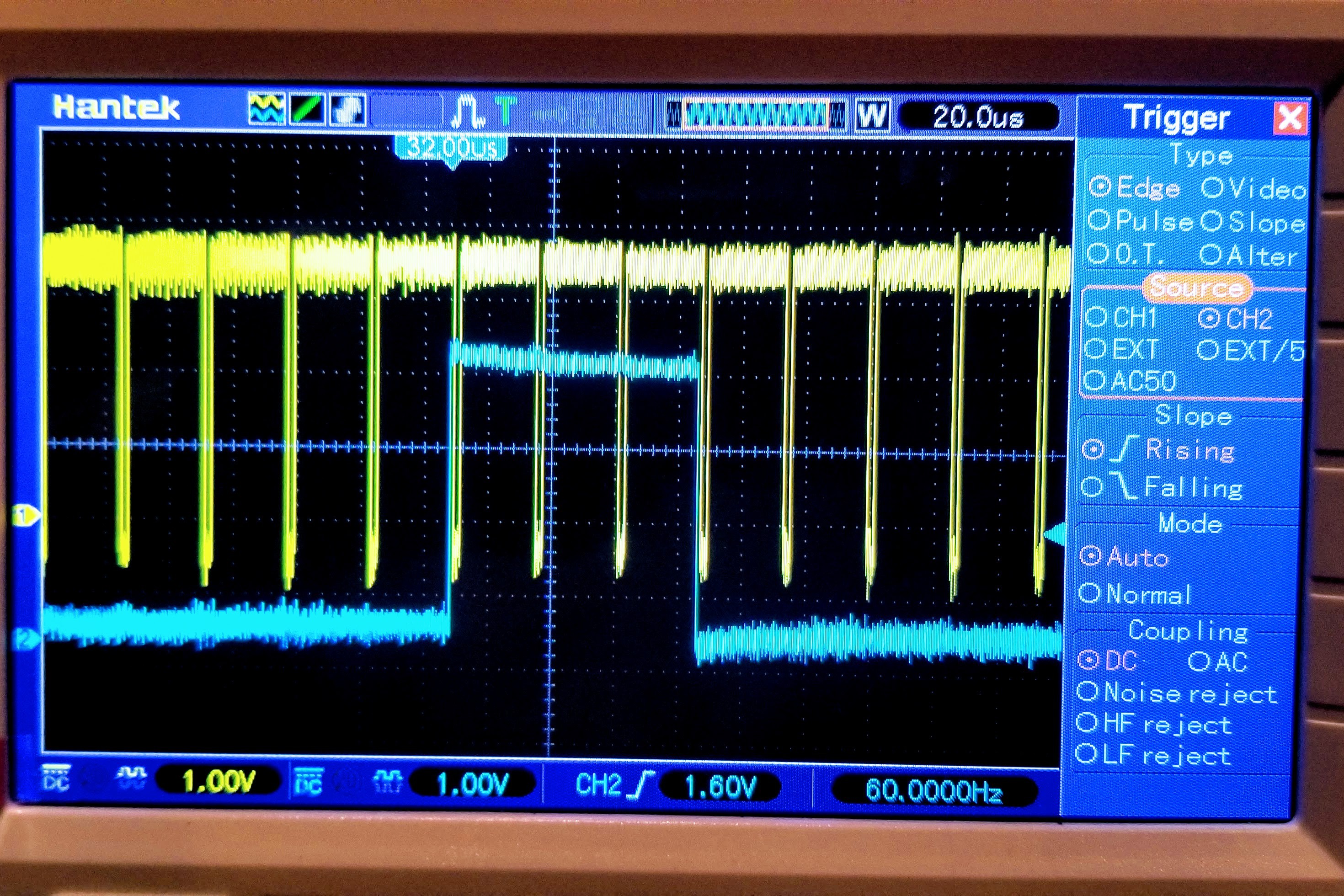
The end result was the 38.4 kHz H-sync and 60 Hz V-sync signals. This matches the modified SVGA timing used with the Arduino in earlier testing. The syncs follow the GTF timing spec with a negative H-sync and a positive V-sync signal spanning three H-sync pulses (as seen below).
![]()
The actual firmware is highly optimized and uses a custom ALU function to return all the video timing based on a single counter and video-specific modulo function. There is still a lot missing from the ALU with only the basic binary functions like ADD, SUB, AND, and OR available, so a multilayer loop was coded to calculate the timing in real time.
A precise cycle count of 208 is required for each iteration of the video loop regardless of any conditional branching that occurs. This is achieved by adjusting the length of the inner loop (shown first in the listing below). This tight 5-cycle loop is used to burn up the remaining cycles given an initial value loaded into the HL register. The other execution paths are padded with NOPs to be divisible by 5 cycles.
The video timing loop uses four bytes of the zero page:
- 0x1FF20: $BURN - temporary store of burn-down count.
- 0x1FF21: $SCAN - line of text glyph to render (0-7)
- 0x1FF22: $LINE - line of video memory to read (0-79)
- 0x1FF23: $SYNC - mask of the V-blank and V-sync bits combined with the scan to make up S register.
The code is located at the reset vector (0x08000) and consists of 109 bytes. The first condition will increment the scan count when the burn loop expires. The V-sync bit is cleared when the scan count is greater than 3. The second condition is met when the count gets to 8 and results in a reset to the scan count and an increment of the line count. The third condition is met when the line count is greater than 75 and results in setting the V-blank and the V-sync bits, where the latter is only set for the first cycle. The final condition is reached when the line count reaches 80 and both the line count and mask are reset to zero.
The listing is show below where the numbers in square brackets represent the number of cycles. The address and encoding is shown along side the nemonic and a comment per instruction.
[2] 8000: 9420 LD Y, 20 [4] 8002: 0804 MVHLZ ND1 # immediate load of $BURN [2] 8004: 9510 LD HL, 10 [3] 8006: 582C SUBH D1Z, ND1 # count down to -1 [2] 8008: A606 LDP PC, 06 # 5-cycle loop, [5n - 1] cycles [2] 800A: 9421 LD Y, 21 [3] 800C: 591F ADDH D1Z, HLD1 # increment $SCAN [2] 800E: 9423 LD Y, 23 [4] 8010: 1E5E ORHL D1Z, SA # strobe scan with $MASK [2] 8012: 9421 LD Y, 21 [2] 8014: 9520 LD HL, 20 [3] 8016: 5C2C SUBH D1Z, NA # compare using $SCAN - 2 [2] 8018: 9423 LD Y, 23 [.] 801A: A5DF LDP HL, DF # clear vsync [3] 801C: B5FF LDN HL, FF # leave vsync [4] 801E: 184C ANDHL D1Z, ND1 # update $SCAN if S > 3 [2] 8020: 9421 LD Y, 21 [2] 8022: 9570 LD HL, 70 [3] 8024: 5C2C SUBH D1Z, NA # compare using $SCAN - 7 [2] 8026: 951F LD HL, 1F # set burn count to 32 (31 + 1) [2] 8028: 8080 NOP; NOP [2] 802A: 80 NOP [2] 802B: B600 LDN PC, 00 # return [49] [2] 802D: 95FF LD HL, FF [4] 802F: 0804 MVHLZ ND1 # immediate load of -1 [2] 8031: 9422 LD Y, 22 [2] 8033: 9510 LD HL, 10 [3] 8035: 5B1E ADDH D1Z, VD1 # increment $LINE [2] 8037: 954B LD HL, 4B [4] 8039: 1D2E SUBHL D1Z, EA # compare using $LINE - 75 [2] 803B: 951A LD HL, 1A # set burn count to 27 (26 + 1) [2] 803D: 8080 NOP; NOP [1] 803F: 80 NOP [2] 8040: B600 LDN PC, 00 # return [48+26] [2] 8042: 954C LD HL, 4C [4] 8044: 1C2C SUBHL D1Z, NA # compare using $SCAN - 76 [2] 8046: 9423 LD Y, 23 [.] 8048: A510 LDP HL, 10 # vsync off [3] 804A: B530 LDN HL, 30 # vsync on [4] 804C: 0804 MVHLZ ND1 # immediate load of $MASK [2] 804E: 9422 LD Y, 22 [2] 8050: 954F LD HL, 4F # set HL to 79 [4] 8052: 1C2C SUBHL D1Z, EA # compare using $LINE - 79, strobe E [2] 8054: 9514 LD HL, 14 # set burn count to 21 (20 + 1) [2] 8056: 8080 NOP; NOP [2] 8058: 8080 NOP; NOP [2] 805A: B600 LDN PC, 00 # return [48+25+31] [2] 805C: 95FF LD HL, FF [4] 805E: 0806 MVHLZ XD1 # immediate load of -1, strobe X [2] 8060: 9423 LD Y, 23 [2] 8062: 9500 LD HL, 00 [4] 8064: 0804 MVHLZ ND1 # immediate load of 0 [2] 8066: 9510 LD HL, 10 # set burn count to 17 (16 + 1) [2] 8068: 8080 NOP; NOP [1] 806A: 80 NOP [2] 806B: 9600 LD PC, 00 # return [48+25+30+21] -
CPU Build Complete
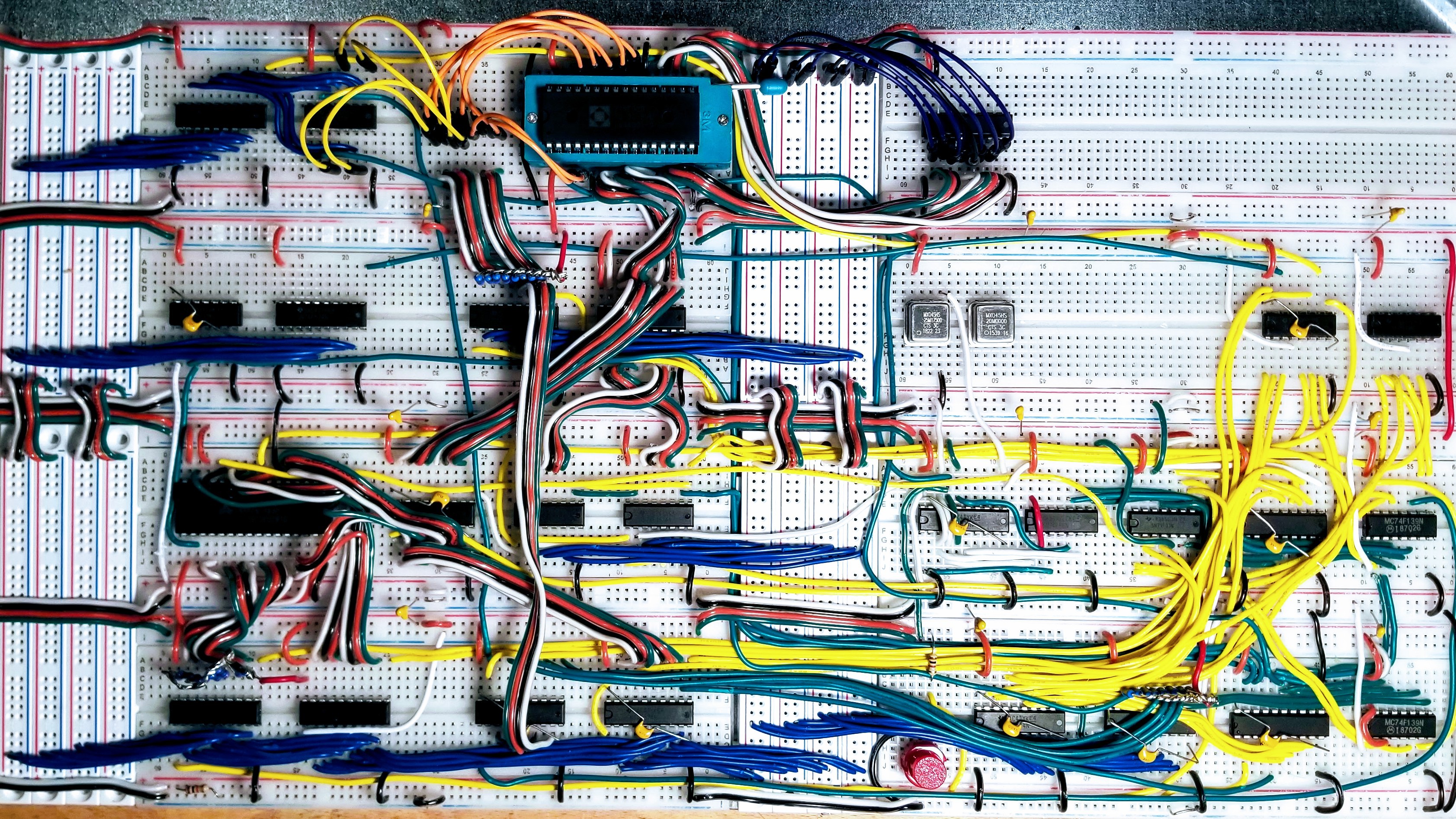
10/15/2019 at 03:50 • 0 commentsQuick update after a long weekend. The final version of the CPU has been built and tested. It's not the prettiest thing in the world!
![]()
There's not much to demo until the GPU is installed. For now, the most exciting thing it has done is generate a 1 Hz pulse. That may sound simple, but this was using a version of the planned RTC code (accurate to 8.5 ppm). It requires 12 bits to divide down the 8 MHz process clock and would normally only use three bytes of the zero page. The version tested used both the zero page and the full RAM address space of bank 0. The ALU operations were also expanded to test the full 2-cycle ALU addition/subtraction instead of just doing increment/decrement.
A couple of notes on the picture: The 70ns NOR flash was having a hard time meeting the 50ns access cycle of the 16 MHz machine clock, so a couple of slower oscillators are being used for testing (the actual OTP ROM is 55ns and should be fine) . There are patch wires on the ROM address and data busses that can be moved to add/remove bus drivers. The current design exceeds the recommended fanout on the data bus, but it doesn't appear to be an issue. In fact the circuit is a lot more stable without them.
-
Video Modes
09/25/2019 at 05:12 • 0 commentsAn early log talked about 16 possible video modes. This is still the case, but a lot has changed since then. The following should clarify what the current modes are and how they are supported.
The 16 modes are defined by 4 bits with the following states:
- Mode0 - Text (0) or Graphics (1)
- Mode1 - Low (0) or High (1) resolution.
- Mode2 - VGA (0) or SVGA (1)
- Mode3 - Mod 16 (0) or Mod 15 (1) timing.
Mode0 is a hardware state (bit 4 of the Eo register) and selects whether the GPU executes one (graphics mode) or two (text mode) machine-cycles per process cycle. The two-machine cycle will complete 80 active process cycles per line, representing 80 characters composed of a code point and color byte. The one-machine cycle completes 160 active cycles, either as 160 single color values (low-res graphics) or 160 nibbles (hi-res graphics).
Mode1 is also a hardware state (bit 5 of the Eo register) and selects whether the 8x8 or 8x16 glyphs are selected from the font ROM. This bit is also used to define the high/low resolution setting for the graphics mode.
Mode2 is used to control the number of lines per frame in software. A low value selects a VGA mode (640x480) at a field rate of 75 Hz using 512 lines per field. A high value selects an SVGA mode (800x600) at a field rate of 60 Hz using 640 lines per field.
Mode3 is also used to control the video timing in software. The number of lines are divided down depending on the video mode and there are two different ways to do this: A low value selects a Mod16, allowing the timing to be divided down by 2, 4, 8, or 16. A high selects a Mod15 allowing the timing to be divided down by 3 or 5. Multiples of 2 are also available to divide down by 6 or 10.
The following tables show all the resolutions available by combining the Mode0 and Mode1 bits for the columns and the Mode2 and Mode3 bits for the rows. The value of the modulo is shown in brackets next to the resolution (%n).
Graphics
(hi-res)Graphics (lo-res)
Text (8x8)
Text (8x16)
VGA%16 320x240 (%2) 160x120 (%4) 80x60 (%8) 80x30 (%16) VGA%15 320x160 (%3) 160x96 (%5) 80x48 (%10) *160x80 (%6) SVGA%16 320x256 (%2) 160x150 (%4) 80x75 (%8) 80x36 (%16) SVGA%15 320x200 (%3) 160x120 (%5) 80x60 (%10) *160x100 (%6)
*Note: Mod15 is not used for the 8x16 glyph text mode, so an additional lo-res graphics mode is defined using a modulo of 6. -
Firmware - part 2
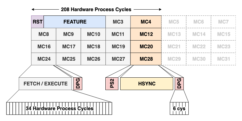
09/14/2019 at 06:08 • 0 commentsThe following shows a breakdown of the firmware process cycle described in the last log. Each cycle spans 4 lines and consists of 5 machine cycles per line:
![]()
The firmware machine cycle consists of 34 hardware process cycles for either the fetch, execute, or horizontal sync. Each machine cycles ends in a decode page jump (DPG) driven by the process cycle state and instruction. This decode takes 6 hardware process cycles resulting in a total length of 40, or 5 uS. Once the fetch is performed, each instruction requires one or two execution cycles. If the instruction is a NOP, then the next instruction is fetched. At the end of the execution cycle the instruction value is set to NOP so that the DPG will jump to fetch.
The 4th machine cycle is reserved for the horizontal sync handling. This also takes 34 hardware process cycles, plus the DPG, and includes an additional 8 cycles for sampling the PS2 port. This is a simple record-and-shift operation performed at the full 38.4 kHz line rate. The PS2 clock and data lines are sampled by two nibbles with the previous sample being shifted. The result after 4 lines is a byte containing 4 bits of the sampled clock and 4 bits of the sampled data. This can be processed to determine what data was received via the port, however, this data is only processed occasionally as described below.
Each firmware process cycle begins with the RST cycle to reset the process state and decide which feature to handle in the following machine cycles. The feature takes up the next one, two, or three machine cycles and can consist of the following:
- Serial communication
- Audio generation
- Keyboard input
The first two are exclusive, so audio can not be generated when serial communication is being handled (sorry, no streaming audio on this machine!). Serial may be full duplex, but could also be handled as half duplex and one of the machine cycles can be given back to the interpreter. The audio takes up two machines cycles and will handle at least two melodic voices and one noise channel. More voices, or ADSR, will be added if there is room when the implementation is finalized.
The keyboard is handled as an additional feature so that serial or audio can be processed concurrently with keyboard input (the latter being required for games). All the serial ports are implemented with hardware flow control, so the keyboard can be suppressed until a keyboard feature cycle is used. The plan is to sample the keyboard 15 times per second, or every 4th refresh at the 60 Hz field rate, or 5th refresh at the 75 Hz field rate. The keyboard input is processed for at least 128 lines, which should allow up to 3 bytes to be read. PS2 devices are required to buffer when the clock is inhibited, so this shouldn't be a problem as long as the user doesn't sustain 15 key presses per second.
PS2 interfaces are also bi-directional and the keyboard requires things like a reset command on power up. These are atypical events and are handled by specialized functions rather than handling during the standard firmware process cycle. The keyboard data transmit function includes the horizontal sync timing but does not run the interpreter. This is to facilitate data transmission at the keyboard's clock rate, which is faster and asynchronous to the 9600 process cycle. This will be fairly rare though (reset, cap lock, setting change) and should only last about 2 milliseconds.
Novasaur CP/M TTL Retrocomputer
Retrocomputer built from TTL logic running CP/M with no CPU or ALU