Alastair Hewitt
-
Single Board?
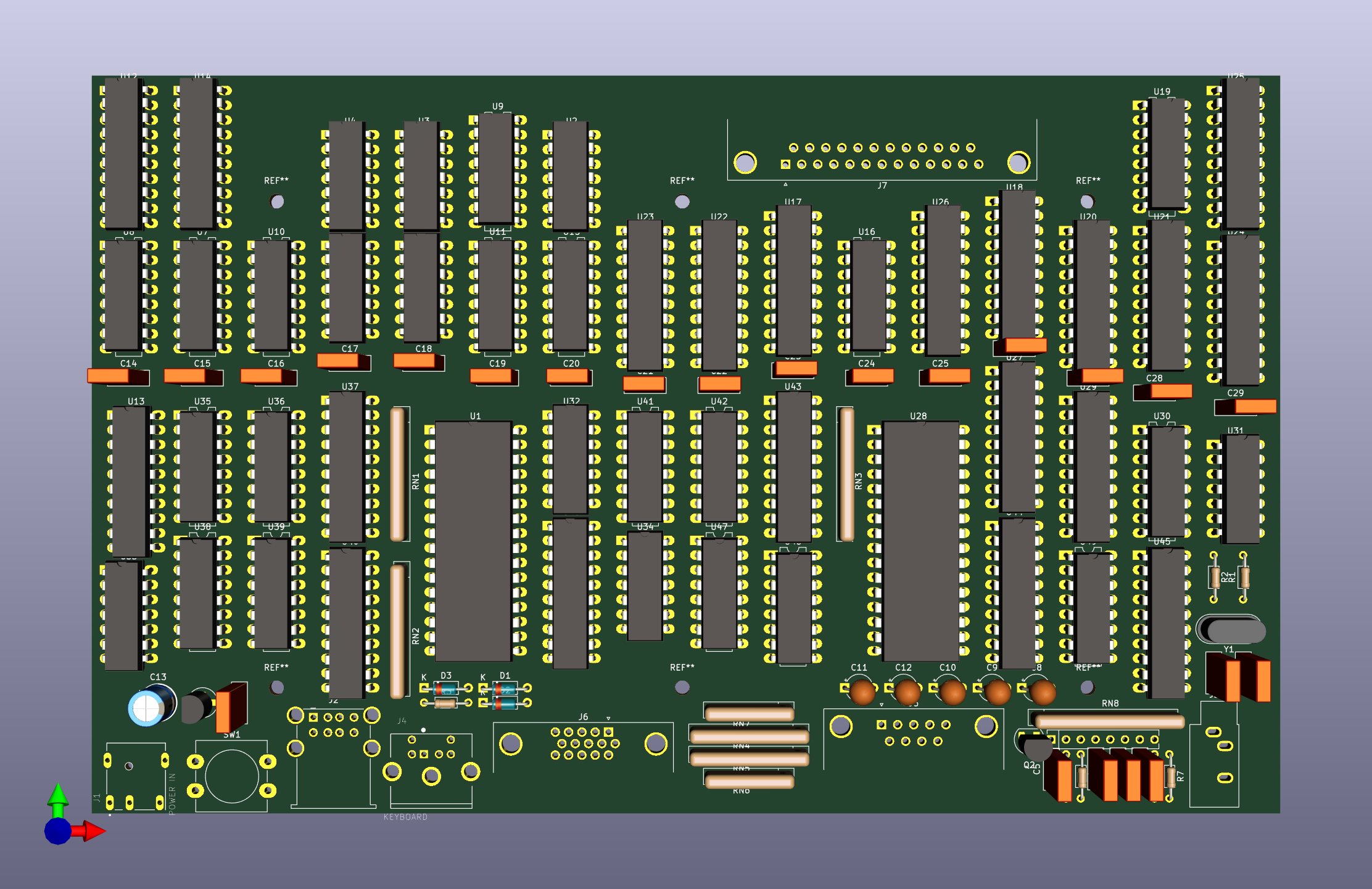
06/03/2019 at 04:50 • 0 commentsA few more minor updates were made to the circuit. The original design used a diode ROM to select the RAM or register that is output to the data bus of the data space. It started out fairly complex, but there were ways to rationalize it by optimizing the instruction encoding. This ROM eventually boiled down to just two 4-input AND gates and it was worth the extra chip to just replace the ROM with a 74F21.
I don't have a 74F21 on hand, so the prototype build got blocked. This provided some time to start on the PCB layout. The original plan was to use two boards with a riser and the schematic showed two pairs of 2x20 headers to join the boards. The board size requirements are starting to drop with the elimination of the diode ROM and a switch to using resistor networks for the video DACs. Switching to a single board would eliminate the risers and save even more room.
The current enclosure will fit a board up to 5" x 8". It now looks possible to squeeze everything on to a single board of this size. An example layout is shown below:
![]()
Not a lot of thought was put in to the layout of the chips, other that to see if they could be placed around the mounting holes a leave a central gap for the decoupling capacitors. The autorouter gave up with this and a lot more thought will be needed to see if it is even possible to configure the board to route at this density. I'll continue along this path though and see if I can make it work.
-
Virtual CPU 2
05/28/2019 at 15:52 • 4 commentsAn initial sketch of the interpreter code has been completed. This was the first time a real program was created using the native machine code. This process exposed some limitations and an optimization in the current design. Changes have been made to the schematic to reflect the following changes:
- The accumulator is always loaded after an ALU function.
- The program counter replaces the accumulator in the set of 8 register targets.
- The dual 4-bit buffer is eliminated from the ECU (-1 chip).
- Additional logic added to support banked RAM (+1 chip).
The hope was to produce something that runs at close to the native speed of the emulated CPU. This will not be possible though. Interpreters are not very efficient and the final implementation will probably operate at around 1/4 of the emulated CPU speed. However, the native machine code can be used to add efficient system calls for accessing and controlling the peripherals (audio/video/serial).
The interpreter uses the zero page to store the virtual CPU registers. These include things like a virtual program counter and stack pointer. Many of these virtual registers are 16 bits and need to be loaded, incremented or decremented, then saved back to the zero page. Additional conditional checking is required to determine if the most significant byte needs to change when the least significant is updated.
Once the program counter is updated the instruction it points to can be read. This will then drive a switch statement to select the code that implements the instruction. There are various ways to make this switch. The most efficient is to use the opcode as an offset to the native program counter. This was the rationale behind the first change above. A custom ALU function can be added to define this offset, but even then, there isn't enough space in a single page to implement all the instruction emulation code.
The current design will use three jumps to select the instruction code. The first will jump within the page to one of several fork points. Each fork then jumps to a new page that branches within that page to specific code that implements the instruction. There is one additional page jump at the end to return to the start of the interpreter loop. The first jump could define up to 64 pages, each of which could contain code for 16 instructions each. This would provide room to support 1024 op codes.
The total overhead for just this instruction decode is around 30 process cycles. The actual instruction implementation would probably require a similar amount of cycles to complete. A total of around 60 cycles per instruction translates to around 0.125 MIPS. This is about 1/4 of an original 1 MHz 68xx processor that could perform around 0.425 MIPS.
The last change listed above is aimed at supporting FUZIX. This is designed for 8-bit CPUs, but requires more than just 64k of RAM. More memory requires Banked RAM to switch between different address spaces. This can be achieved on the YATAC by using the extended register to define additional address bits for the RAM. Two bits are used to support four address spaces, with the GPU automatically switching to the highest bank to access the display RAM.
-
Virtual CPU
05/23/2019 at 02:37 • 0 commentsThe project is 3 months old. The CPU is running and boots up correctly. All the timing has been optimized and operates at up to 32 MHz (requiring a 64 MHz dot clock). The project even made it to the front page.
So far about 40% of the circuit has been built and tested on breadboard. The design is now finalized enough to commit to a proper CAD drawing of the schematic. This took several days to complete, which explains why the breadboard has stalled at 40%. It will take at least another month to finish the build and get the GPU generating a video signal. The initial PCB routing will start in parallel, so that may be completed around the same time.
The software design is also starting to pick up pace. This machine follows a similar design to the Gigatron in using the Harvard Architecture. There are two separate address spaces for both the ROM and the RAM. The ROM owns the Program Space identified in the schematic using the PA[0..15] and PD[0..7] bus labels. The RAM owns the Data Space identified in the schematic using the DA[0..15] and DD[0..7] bus labels. Only code in ROM can be executed and only data in the RAM can be accessed.
The machine code is designed to be more like a microcode rather than something you would use to write general purpose programs with. These low-level instructions can be combined to build up a more expressive instruction set in the context of a virtual machine. This machine would have the more familiar Von Neumann Architecture where both the code and data exist in the same Data Space of the underlying Harvard Architecture.
The plan is to take an existing CPU and build a virtual machine to be binary compatible with it, rather than design a new instruction set from scratch. The main advantage with this approach is to leverage existing tool chains and software for that processor. In theory, an existing C compiler for that processor can be used to build executable code, which would greatly reduce the software development overhead.
My inclination is towards something in the 68XX family. These have a simple elegance that should translate well to the VM. The current target CPU is the 6809 and might include some or all of the 6811. There is also a lot of retro love for the 6502 and it may be possible to have a reduced 6502 mode. All the CPUs in the 8-bit Motorola lineage share a lot in common, so it's just a variation on a theme.
-
ALU and Instruction Set
05/13/2019 at 15:19 • 0 commentsHardware testing is complete on all the jump and branch instructions. So that's the first 8 out of 256 instructions tested! The next 24 are loading operands. These should work fine since the jump/branch instructions are also loading operands in order to update the PC and Pg register. All the rest are ALU instructions, so it's time to work on the build script to generate the 96k of lookup tables.
First off is to define the functions. There's room for 8 full byte-wide, 4 half nibble-wide, and 64 unary functions. One of the unary functions has to be the identity (do nothing) so I don't count that in the total of 75 functions.
The 8 byte-wide functions are the classics:
- ADD - Addition
- DAD - BCD addition
- SUB - Subtraction
- DSB - BCD subtraction
- AND - Logical AND
- OR - Logical OR
- XOR - Logical Exclusive-OR
- CMP - Compare (returns 0 if equal, else -1)
The 4 nibble-wide functions are used for multiplication, division, and modulo. These would be used to multiply two nibbles to get a byte, or divide a byte by a nibble to get a nibble.
The 64 unary functions are contained in 4 sets of 16. One of these could contain math related functions consisting of the following:
- SQRT - Square Root
- POW2 - Square (x**2)
- POW3 - Cube (x**3)
- INV - 1/x
- SIN - sin(x)
- ASIN - arc sin(x)
- COS - cos(x)
- ACOS - arc cos(x)
- TAN - tan(x)
- ATAN - arc tan(x)
- EXP - e**x
- LN - natural log(x)
- LOG - base 10 log(x)
- LOG2 - base 2 log(x)
- ABS - absolute (remove sign)
- ?? - ran out of ideas :(
These math functions may look impressive, but they have a very limited dynamic range at only 8 bits wide. These can not be used directly to build a real floating-point library, but they can provide short cuts in making a real library faster. They could be used directly for demo-grade things like a Mandelbrot program, or to draw a circle on the screen. The circle should be clean if the radius is kept below 128, which is realistic in both the low and hires graphics modes.
The other sets would contain functions related to graphics, serial communication, keyboard scan codes, interpreter jump offsets etc. I have some ideas, but not worth finalizing at this point. The last set (FN3/FNH) are the most used and contain the typical unary functions you would see on other processors:
- INC - Increment (x+1)
- DEC - Decrement (x-1)
- INC2 - Double Increment (x+2)
- DEC2 - Double Increment (x-2)
- 1COM - One's complement (invert bits)
- 2COM - Two's complement (invert bits + 1)
- ROR - Rotate Right
- ROL - Rotate Left
- LSR - Logical Shift Right
- LSL - Logical Shift Left
- ASR - Arithmetic Shift Right
- ASR4 - Arithmetic Shift Right by 4 (move upper nibble to lower preserve sign)
- SR4 - Shift Right by 4 (move upper nibble to lower)
- SL4 - Shift Left by 4 (move lower nibble to upper)
- SWAP - Swap nibbles
- IDEN - Identity function (x = x)
The instruction set can now be derived based on the functions defined above. The following lists all 256 instructions:
00: NOP 01: JMP D 02: BPZ D 03: BN D 04: PJ D 05: PJT D 06: PBPZ D 07: PBNT D 08: LD PC, D 09: LD V, D 0A: LD X, D 0B: LD Y, D 0C: LD HL, D 0D: LD E, D 0E: LD EX, D 0F: LD EY, D 10: LDZ PC, D, RAM1 11: LDZ V, D, RAM1 12: LDZ X, D, RAM1 13: LDZ Y, D, RAM1 14: LDZ HL, D, RAM1 15: LDZ E, D, RAM1 16: LDZ EX, D, RAM1 17: LDZ EY, D, RAM1 18: LDZ PC, D 19: LDZ V, D 1A: LDZ X, D 1B: LDZ Y, D 1C: LDZ HL, D 1D: LDZ E, D 1E: LDZ EX, D 1F: LDZ EY, D 20: ADD A, HL, RAM0 21: DAD A, HL, RAM0 22: SUB A, HL, RAM0 23: DSB A, HL, RAM0 24: AND A, HL, RAM0 25: OR A, HL, RAM0 26: XOR A, HL, RAM0 27: CMP A, HL, RAM0 28: ADD RAM0, HL 29: DAD RAM0, HL 2A: SUB RAM0, HL 2B: DSB RAM0, HL 2C: AND RAM0, HL 2D: OR RAM0, HL 2E: XOR RAM0, HL 2F: CMP RAM0, HL 30: ADD A, HL, RAM1 31: DAD A, HL, RAM1 32: SUB A, HL, RAM1 33: DSB A, HL, RAM1 34: AND A, HL, RAM1 35: OR A, HL, RAM1 36: XOR A, HL, RAM1 37: CMP A, HL, RAM1 38: ADD A, HL 39: DAD A, HL 3A: SUB A, HL 3B: DSB A, HL 3C: AND A, HL 3D: OR A, HL 3E: XOR A, HL 3F: CMP A, HL 40: FNH A, PC, RAM0 41: FNH A, V, RAM0 42: FNH A, X, RAM0 43: FNH A, Y, RAM0 44: FNH A, HL, RAM0 45: FNH A, E, RAM0 46: FNH A, EX, RAM0 47: FNH A, EY, RAM0 48: FNH RAM0, PC 49: FNH RAM0, V 4A: FNH RAM0, X 4B: FNH RAM0, Y 4C: FNH RAM0, HL 4D: FNH RAM0, E 4E: FNH RAM0, EX 4F: FNH RAM0, EY 50: FNH A, PC, RAM1 51: FNH A, V, RAM1 52: FNH A, X, RAM1 53: FNH A, Y, RAM1 54: FNH A, HL, RAM1 55: FNH A, E, RAM1 56: FNH A, EX, RAM1 57: FNH A, EY, RAM1 58: FNH A, PC 59: FNH A, V 5A: FNH A, X 5B: FNH A, Y 5C: FNH A, HL 5D: FNH A, E 5E: FNH A, EX 5F: FNH A, EY 60: FNH X, PC, RAM0 61: FNH X, V, RAM0 62: FNH X, X, RAM0 63: FNH X, Y, RAM0 64: FNH X, HL, RAM0 65: FNH X, E, RAM0 66: FNH X, EX, RAM0 67: FNH X, EY, RAM0 68: FNH X, PC 69: FNH X, V 6A: FNH X, X 6B: FNH X, Y 6C: FNH X, HL 6D: FNH X, E 6E: FNH X, EX 6F: FNH X, EY 70: FNH RAM1, PC, RAM1 71: FNH RAM1, V, RAM1 72: FNH RAM1, X, RAM1 73: FNH RAM1, Y, RAM1 74: FNH RAM1, HL, RAM1 75: FNH RAM1, E, RAM1 76: FNH RAM1, EX, RAM1 77: FNH RAM1, EY, RAM1 78: FNH E, PC 79: FNH E, V 7A: FNH E, X 7B: FNH E, Y 7C: FNH E, HL 7D: FNH E, E 7E: FNH E, EX 7F: FNH E, EY 80: ADD A, L, RAM0 81: DAD A, L, RAM0 82: SUB A, L, RAM0 83: DSB A, L, RAM0 84: AND A, L, RAM0 85: OR A, L, RAM0 86: XOR A, L, RAM0 87: CMP A, L, RAM0 88: ADD RAM0, L 89: DAD RAM0, L 8A: SUB RAM0, L 8B: DSB RAM0, L 8C: AND RAM0, L 8D: OR RAM0, L 8E: XOR RAM0, L 8F: CMP RAM0, L 90: ADD A, L, RAM1 91: DAD A, L, RAM1 92: SUB A, L, RAM1 93: DSB A, L, RAM1 94: AND A, L, RAM1 95: OR A, L, RAM1 96: XOR A, L, RAM1 97: CMP A, L, RAM1 98: ADD A, L 99: DAD A, L 9A: SUB A, L 9B: DSB A, L 9C: AND A, L 9D: OR A, L 9E: XOR A, L 9F: CMP A, L A0: ADD X, L, RAM0 A1: DAD X, L, RAM0 A2: SUB X, L, RAM0 A3: DSB X, L, RAM0 A4: AND X, L, RAM0 A5: OR X, L, RAM0 A6: XOR X, L, RAM0 A7: CMP X, L, RAM0 A8: ADD X, L A9: DAD X, L AA: SUB X, L AB: DSB X, L AC: AND X, L AD: OR X, L AE: XOR X, L AF: CMP X, L B0: ADD RAM1, L, RAM1 B1: DAD RAM1, L, RAM1 B2: SUB RAM1, L, RAM1 B3: DSB RAM1, L, RAM1 B4: AND RAM1, L, RAM1 B5: OR RAM1, L, RAM1 B6: XOR RAM1, L, RAM1 B7: CMP RAM1, L, RAM1 B8: ADD E, L B9: DAD E, L BA: SUB E, L BB: DSB E, L BC: AND E, L BD: OR E, L BE: XOR E, L BF: CMP E, L C0: MUL A, L, RAM0 C1: DML A, L, RAM0 C2: DIV A, L, RAM0 C3: MOD A, L, RAM0 C4: FN0 A, L, RAM0 C5: FN1 A, L, RAM0 C6: FN2 A, L, RAM0 C7: FN3 A, L, RAM0 C8: MUL RAM0, L C9: DML RAM0, L CA: DIV RAM0, L CB: MOD RAM0, L CC: FN0 RAM0, L CD: FN1 RAM0, L CE: FN2 RAM0, L CF: FN3 RAM0, L D0: MUL A, L, RAM1 D1: DML A, L, RAM1 D2: DIV A, L, RAM1 D3: MOD A, L, RAM1 D4: FN0 A, L, RAM1 D5: FN1 A, L, RAM1 D6: FN2 A, L, RAM1 D7: FN3 A, L, RAM1 D8: MUL A, L D9: DML A, L DA: DIV A, L DB: MOD A, L DC: FN0 A, L DD: FN1 A, L DE: FN2 A, L DF: FN3 A, L E0: MUL X, L, RAM0 E1: DML X, L, RAM0 E2: DIV X, L, RAM0 E3: MOD X, L, RAM0 E4: FN0 X, L, RAM0 E5: FN1 X, L, RAM0 E6: FN2 X, L, RAM0 E7: FN3 X, L, RAM0 E8: MUL X, L E9: DML X, L EA: DIV X, L EB: MOD X, L EC: FN0 X, L ED: FN1 X, L EE: FN2 X, L EF: FN3 X, L F0: MUL RAM1, L, RAM1 F1: DML RAM1, L, RAM1 F2: DIV RAM1, L, RAM1 F3: MOD RAM1, L, RAM1 F4: FN0 RAM1, L, RAM1 F5: FN1 RAM1, L, RAM1 F6: FN2 RAM1, L, RAM1 F7: FN3 RAM1, L, RAM1 F8: MUL E, L F9: DML E, L FA: DIV E, L FB: MOD E, L FC: FN0 E, L FD: FN1 E, L FE: FN2 E, L FF: FN3 E, L -
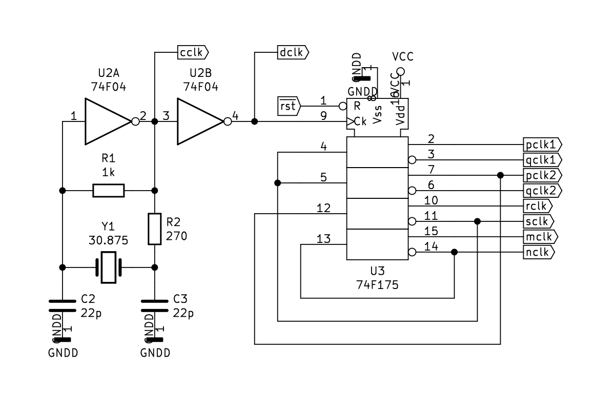
Clock Circuit
05/09/2019 at 02:35 • 0 commentsThe clock circuit consists of a Pierce Oscillator running at 30.875 MHz and two Johnson Ring Counters. The first ring counter (mclk/nclk) consists of a single flip-flop to divide the 30.875 MHz dot clock (dclk) down by a factor of 2. The second (pclk/qclk) consists of two flip-flops to divide the dot clock down by a factor of 4. The last stage of this counter is duplicated to provide an additional set of identical clocks.
![]()
Some considerations in this design:
- A single clock source is used to derive all the other clocks, rather than feeding the clock of one flip-flop with the output on another. This keeps all the clock edges aligned.
- The rising edges of the mclk and the pclk/qclk must to be synchronized. This requires the flip-flops to be reset on initialization or after power fluctuation.
- The pclk and qclk control complementary bus contexts. The complementary outputs of a single flip-flop keeps these perfectly symmetrical and avoids bus contention, especially when held in reset.
- The pclk and qclk are both used 11 times throughout the circuit and this exceeds the maximum TTL fanout for a single output. Two sets of these clocks are generated and divided evenly so no one clock output serves more than 6 inputs.
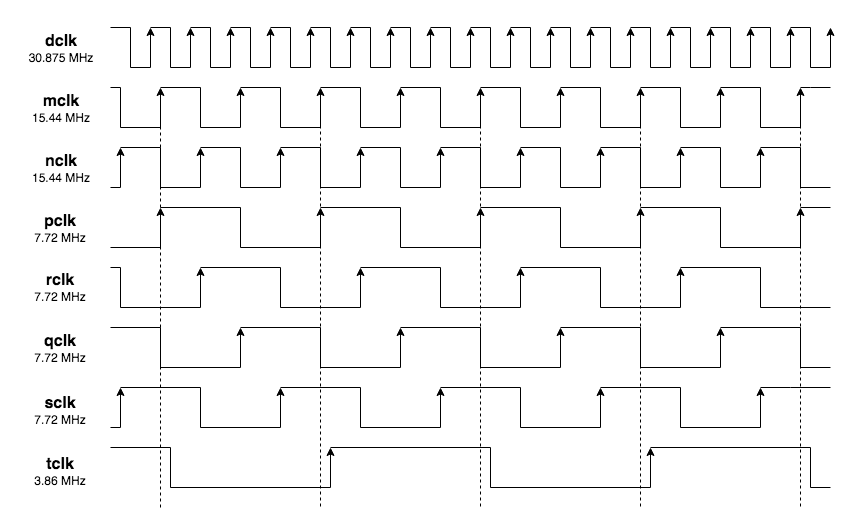
The following shows the clocks generated by the circuit above. The tclk is also included for reference, but not shown in the circuit.
![]()
-
Overclocking
05/09/2019 at 02:02 • 0 commentsOverclocking usually happens after a project is complete. This one started with overclocking and the design was adapted from the outset to maximize performance. The results have been impressive.
The original goal was to use the standard VGA dot clock of 25.175 MHz. This was divided by two to generate a machine clock of around 12.5 MHz. Calculations showed this would work fine for 55ns memory, but not for the 70ns NOR flash being used in development. It looked like that wouldn't make it past 11 MHz.
However, it appears the memories are capable of significantly better performance than their quoted specs. The current design was able to support a machine clock as high as 19 MHz with NOR flash (two different types were tested). Faster memories (10ns) would easily support a machine clock in the 30-35 MHz range, so a dot clock as high as 70 MHz may be possible. The clock circuit and state machine were tested with a dot clock as high as 100 MHz and both performed well, but the NOR flash was basically a random number generator at that speed!
The plan is to use era-appropriate memory speeds for the late 70's though. This doesn't mean if a single 1,024 bit memory could do 25ns on its own, then I can use 25ns memory. It needs to be a memory sub-system of equivalent size, which could require up to a 1,000 chips to store 128k bytes in 1978. The fastest memory sub-system of that size and era would probably come out of a Cray-1 super computer. The Cray-1 memory system was capable of a 50ns access time, so that seems like the appropriate speed limit for this design.
This works out at around 30 MHz for the dot clock and a machine clock of 15 MHz. Another consideration in selecting the exact frequency is the serial communication. The margin of error in syncing with a monitor is much greater than a high-speed serial link. A UART frequency is therefore more important than a dot-clock frequency. Plus, it's almost impossible to get the old-school VGA crystals these days.
There's two options in the 30 MHz range. Both divide down to 115,200 baud in a whole number of process cycles (1/4 of the dot clock):
- 29.4912 MHz = 64 process cycles * 115,200
- 30.875 MHz ~ 67 process cycles * 115,200
The plan is to use the higher frequency, but the slower option may be used depending on stability of the final design. The higher frequency is 22.6% faster than the standard VGA dot clock, so the GPU horizontal scan length is increased from 200 to 244 process cycles. The active screen memory per line is increased from 160 bytes to 192 bytes. This increases the text mode from 80 to 96 columns.
-
Progress
04/29/2019 at 19:17 • 0 commentsThe redesign is complete and everything has changed. I'll need to go back and update all the logs because most of that information is no longer valid. Things have been rationalized and the timing simplified. This has resulted in an even faster machine that could potentially run on the higher VESA dot clock of 31.5 MHz. More on that after some more testing.
The big change was getting rid of the clock and strobe timing. The clocks control the bus context and the strobes were used to latch data within the bus timing. A strobe would be 6ns before the end of the bus cycle to allow time to hold the latched data before the context switch.
This wasn't needed though because the ROM owns its data bus. Data from the previous context can be left on the bus after the switch from the GPU to CPU. The bus tri-state takes at least 3ns to change the address and the ROM is guaranteed to hold the data for at least 7ns after that. Since the data will stick around on the bus for at least 10ns then the same clock used for the bus control can be used to latch the data, even after one-layer of logic delay. This effectively overlaps the clock cycles and time can be borrowed from the next cycle to extend the previous one.
The build is finally starting to take shape. Things are progressing slowly since everything is being validated at every step. Bus contention is also being checked and one issue was resolved that would happen on reset. The new clock circuit needs to be reset to synchronize two independent ring counters. If the clocks are all pulled low then both bus contexts exist at the same time. This effectively shorts any TTL output that is driving a high on to the same bus line as something holding it low. The new circuit uses flip-flops with complementary outputs to prevent this.
The picture below shows the bare-bones CPU (ROM not shown). This contains the main clock generator, CPU state machine, Program Counter and bus buffer, Instruction register, and a little bit of logic (not all wired up in this picture). There's also an additional register to drive something on the bus during the GPU bus cycle.
![]()
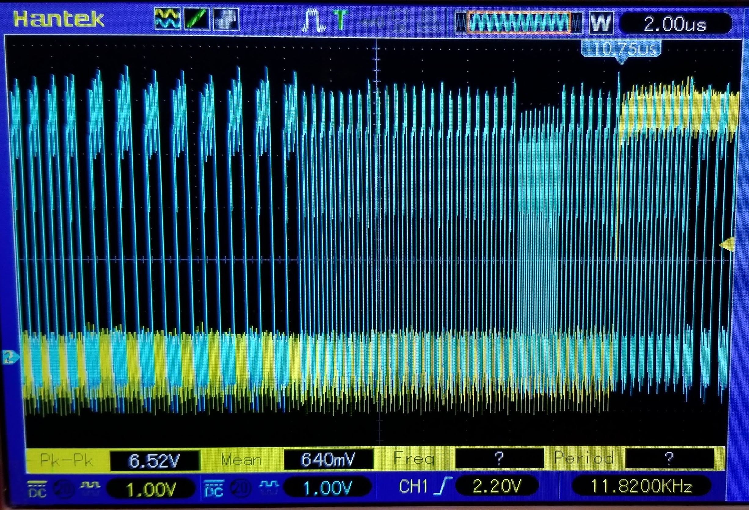
The ROM was programmed with sequential groups of 16 instructions. The instruction sequences demonstrate different execution cycles. The oscilloscope output below shows the least significant bit of the Program Counter. Going from left to right you can see cycles where the PC is incremented every 4 machine cycles, then every 6, every 2, and then every 1 cycle before going back to 2, then 4.
![]()
The instructions executed above are:
- Short ALU - 4 cycles between PC increments
- Long ALU - 6 cycles between PC increments
- Load Zero-page - 2 cycles between PC increments
- Load Operand - 2 cycles between PC increments
- Page Jump (unconditional) - 2 cycles between PC increments
- Jump (condition not met) - 1 cycle PC increment
- Jump (unconditional) - 2 cycles between PC increments
- NOP - 2 cycles between PC increments
Next up is a jump program that will reload the Program Counter and execute a loop. Then add the accumulator and program some ALU functions.
-
CPU State Machine
04/22/2019 at 15:57 • 1 comment8 weeks in and the CPU is running, although it's not doing anything useful yet. The initial task was to get all the timing circuits in place and measure the performance of the system.
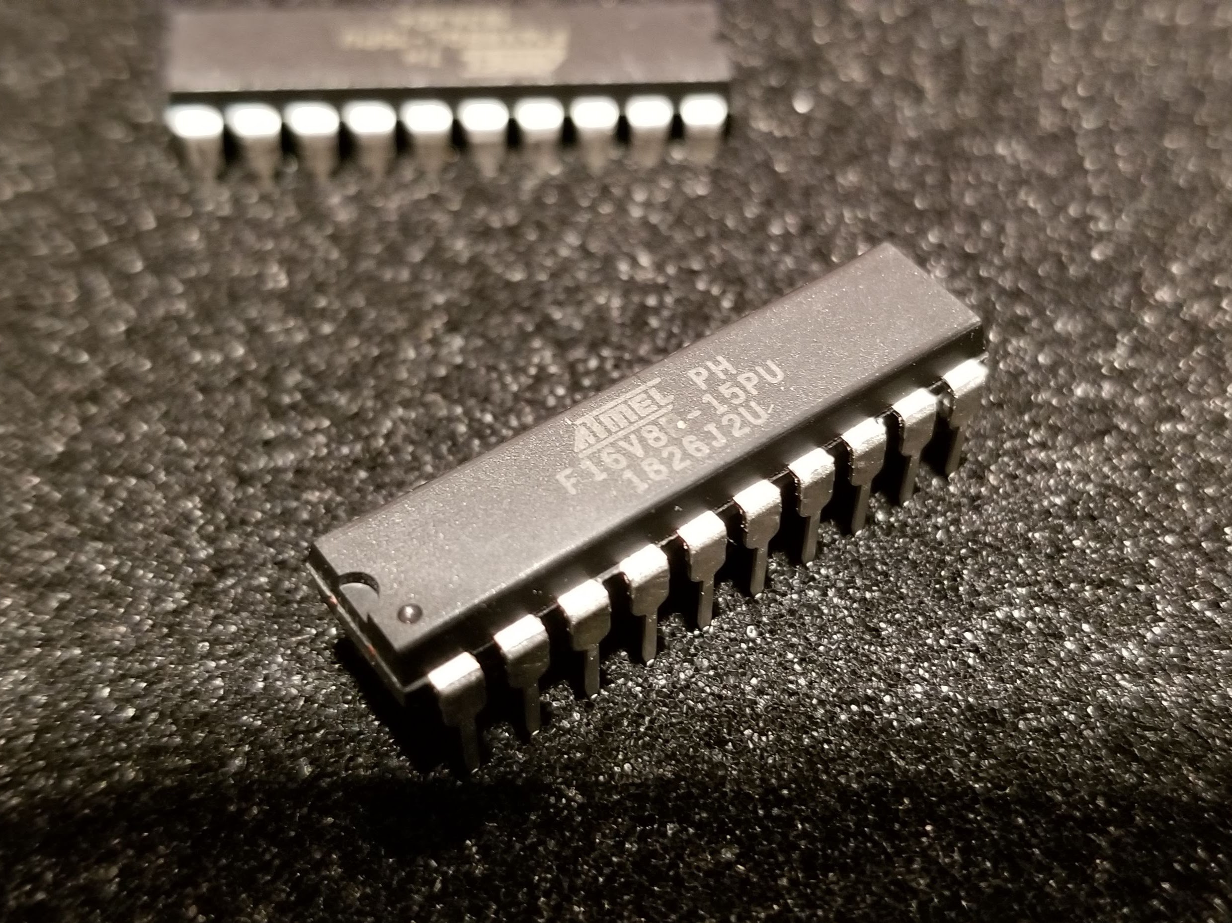
Only 10 chips are needed to implement the clock circuit, program counter, instruction register, and CPU state machine. This would have been 15 chips if it wasn't for this guy below.
![]()
The initial design was all 74-series chips and it needed 50 in total. A single programmable array logic (PAL) can absorb 6 of the 74-series chips. The first PALs were introduced in 1978 and included the 16R8. The device show above is the modern equivalent knows as a GAL (generic array logic). This chip can emulate a variety of old PAL devices and in this case it is being used as the 1978-era 16R8.
I could go further though. The table below shows the possible chip count reductions using more PALs:
PALs TTL Other Total Original Design 0 50 5 55 Current Design 1 44 5 50 Optional Design 5 30 5 40 The optional design would replace the 8-bit counters that currently require 3 chips (two 4-bit counters + buffer) with a single chip. There would be 3 of these 8-bit counter PALs. The rest of the instruction decode logic and bus state machine would also fit in a single PAL. Note: Control signals used by the counters would require the larger 24-pin 22R10 devices.
Consolidating 6 chips in to one was an easy choice. The current plan is to stop there though. The design files for the PAL have been uploaded along with a simulation showing different execution states for the CPU State Machine.
-
Internet
04/18/2019 at 14:07 • 2 commentsThis was always a stretch goal, but it looks very doable now the design is complete... and it wouldn't be the first TTL Computer on the Internet.
What is the scope of Internet-enabled?
Connectivity is via the RS232 port. This provides an ancient but still supported interface standard. There are plenty of inexpensive options to adapt to more modern serial standards. These include USB with an FTDI cable and Ethernet with a WizNet protocol adapter. Of course, dial-up would be the most authentic method using a standalone modem.
A TCP/IP stack is a project in its own right. Something like uIP could be ported to the YATAC and would work within the constrained resources. Things like the WizNet adapter can offload some of this stack overhead and will be used to get things up and running quickly.
The simplest server/client model would be TFTP. I plan to do better than this though and go straight to HTTP with a browser and web server. However, this would be the Tim Berners-Lee 1991 version of the Web: Text only browser supporting a subset of HTML 2.0 and basic web server file handling. This will provide everything needed to upload and download programs via a web interface, so no mass storage is needed.
The hardware text mode was specifically designed to render basic web pages. The 4 fonts are used with HTML as follows:
- Standard font used to render text body.
- Bold font used for <b> tags.
- Italic font used for <i> tags.
- Underline font used for <u> and <a> tags.
There are 8 colors available, so links would be highlighted along with using the underline font. Headers would also be highlighted in a different color using the bold font.
Pages can be up to 256 lines long and are rendered directly to the screen memory. Scrolling is achieved by updating one register on every screen refresh. Almost no additional CPU resources are required to display a page once loaded.
-
Redesign
04/14/2019 at 23:44 • 4 commentsSo there's the easy problem (designing a computer out of TTL) and then there's the hard problem (make it work at 12.5 MHz).
I was close, but not quite there. The RAMDAC was hitting the wall with a dot clock above 21 MHz. I have to simplify the logic that switched between the 16 and 8 colors in text mode. I have to take the ZX Spectrum approach and drop to 15 colors with a subtractive intensity rather than additive.
The instruction decode looked good on paper but I forgot about the 10 ns propagation from the clock to output of the instruction register. I was able to find a solution but the entire decode path barely fits in the 80 ns machine cycle. Too much parasitic capacitance in a PCB layout and things will get glitchy once the chips reach a toasty 70 C.
So I've been shuffling things around and doing some consolidation. I'm back to a solid design, but I will need to redraw the schematic. I'm not spending another weekend doing that by hand, so the next schematic will be a proper CAD drawing. But saying that, it's time to start building and verifying this thing will work at these speeds. Only then is it worth documenting the verified design.
Not surprisingly the first thing to test is the clock and bus control state machine. After that the instruction decode and CPU state machine. I'll then be able to run a simple jump/loop program. It won't be Turing Complete, but if that program runs reliably at 12.5 MHz then everything else will work. I can then start on the fun stuff like adding RAM and the video output. Then the really hard problem (software).
Novasaur CP/M TTL Retrocomputer
Retrocomputer built from TTL logic running CP/M with no CPU or ALU