I have known about JLCPCB for a while and thought of giving them a try for this project. The PCB is a small one and to save money I thought of panelizing the PCB. I'll have more PCBs for the same price. YAY. There was only one problem, I had no idea how to go about it. I went off to google and searched. I got a couple of cool options. Some easy and others not so easy.
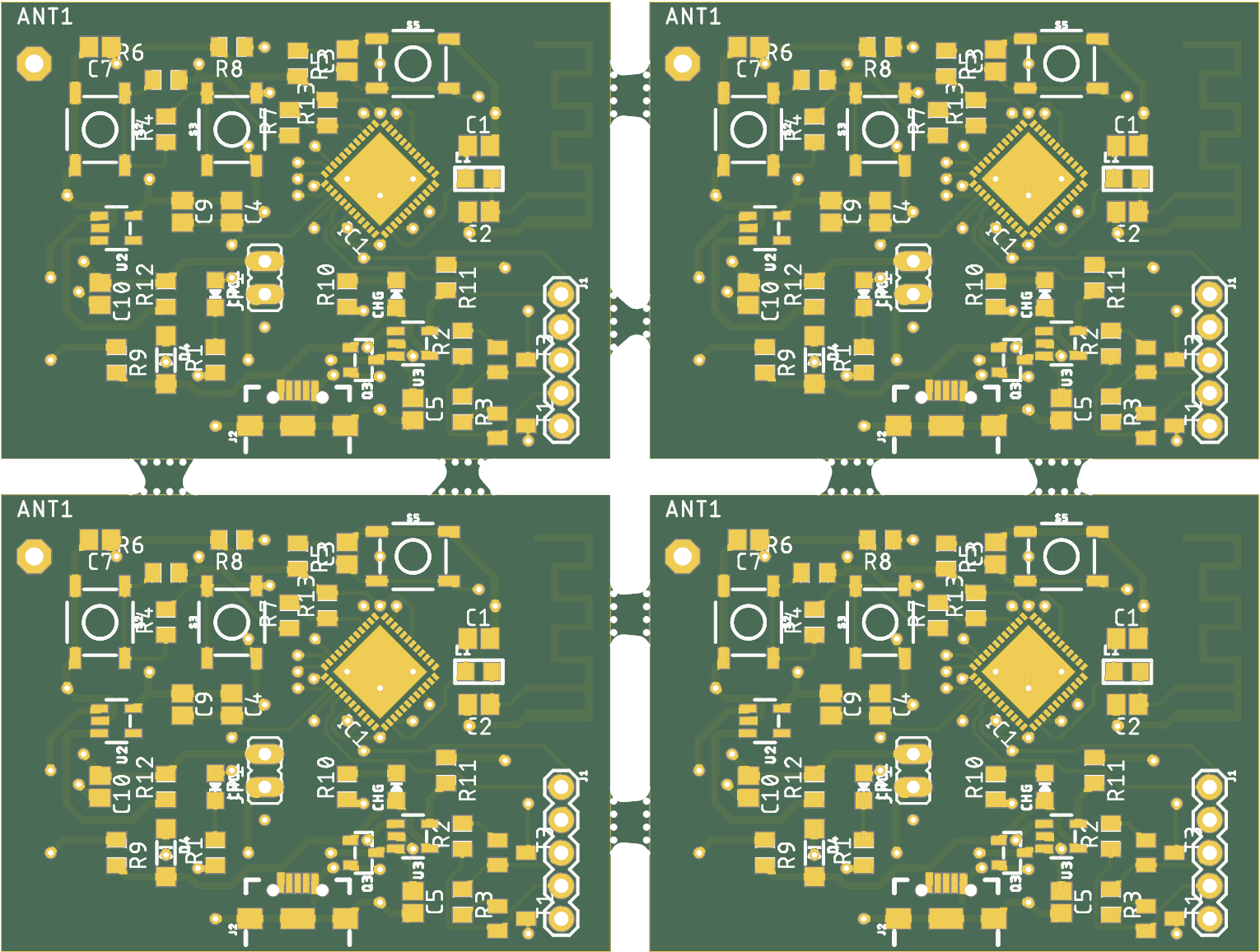
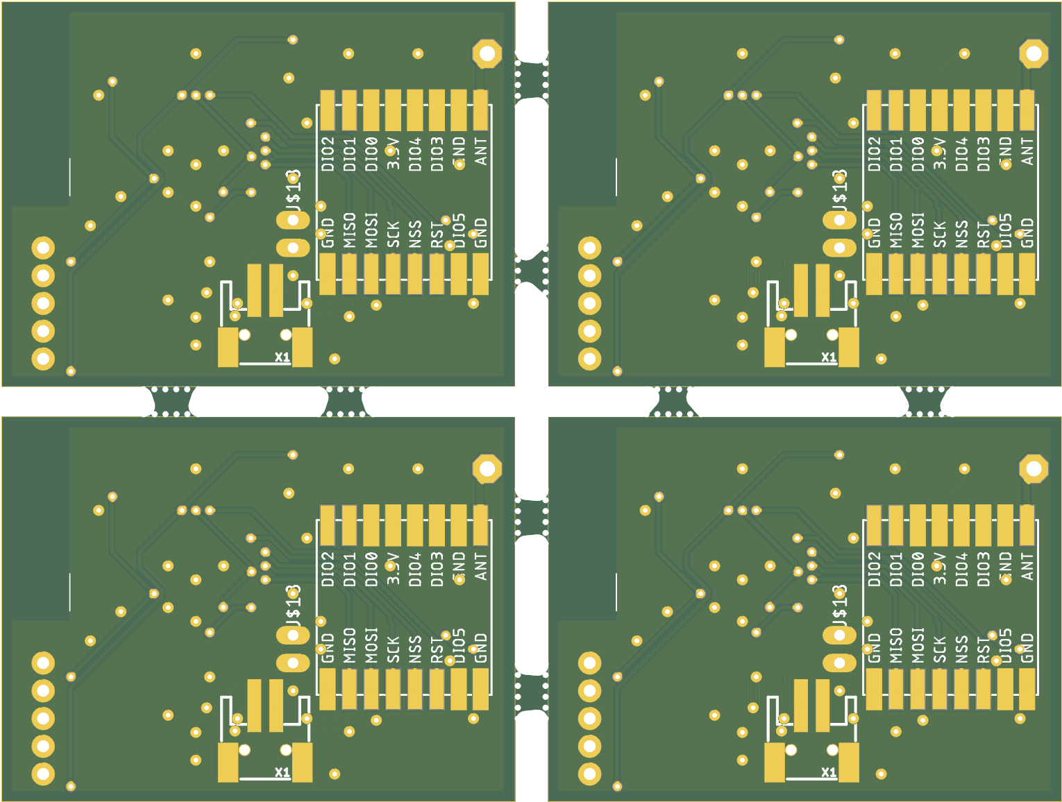
After deliberating with google and very helpful guys on the HackChat, I settled for GerberTools (https://github.com/ThisIsNotRocketScience/GerberTools/releases). This awesome application has a cool GUI and quite efficient gerber Panelizer. I took me a while to get the hang of it for I had dimensioned my board on the copper layer (yeah, who does that?). I finally got it to work by removing the dimension and using DirtyPCB's cam files on eagle after it turned out that the app was no fan of the .gbr format. Below is the result I got after panelizing


Notice the absence of traces in the bottom layer. Thats a bug I hope the maker of the gerber viewer fixes. I displayed it quite well on JLCPCBs gerber viewer though. Well, I am sure the PCB is very well on its way down and will be available in a few weeks.
NB. I'll update the PCB file again (Sorry)
 Taiwo
Taiwo
Discussions
Become a Hackaday.io Member
Create an account to leave a comment. Already have an account? Log In.
JLCPCB didn't charge any more than the regular. Use the program (https://github.com/ThisIsNotRocketScience/GerberTools/releases) and don't worry about anything.
Are you sure? yes | no
Thanks that's good to know.
Are you sure? yes | no
Did you go with JLCPCB? Did they charge extra because you panelised it? Their web page is a bit ambiguous about the issue:
https://support.jlcpcb.com/article/49-pcb-panelization
On one hand they say:
1. Note: This additional charge only applies if the PCBs on a panel are different. Boards such as in the left hand image below will not incur an additional charge because they are easy to pick up but boards such as in the right hand image would incur an additional charge.
On the other hand befor that they say:
2. Similarly, using holes or slots as break off sections between boards are treated the same way as putting more than one design on a panel, each with its' own board outline.
Then they go on to suggest drawing some lines on the silk screen so that you can separate them yourself, but this would require me to have a dremel.
So which is it? If I use slots and mousebites to put 2 of the same design inside 100x100 mm, will they invoke rule 2? I suppose I could submit it and see what their sales engineers say.
Are you sure? yes | no