In my last log, I talked about how I was getting started with PLDs in hopes of replacing the 7400-series chips that made up my address decoder. I'm pleased to report that I refined the CUPL code for the ATF16V8B I'd bought, and the chip is now on the board and working perfectly.
This has brought multiple wins to the project - I've saved a fair bit of board space (8 7400-series have been removed) so the eventual PCB fab will be cheaper, power requirements are lessened, and I've finally been able to fix some bugs in the original decoder design (e.g. gating everything off with /AS and /IACK meaning less additional support circuitry is needed). This also means that /EXPSEL now works as I originally intended.
The rough CUPL code I posted last time has been considerably cleaned up (it was originally a dump from Logisim's combinatorial analysis). The main logic for the six output pins looks like this:
!EVENRAMSEL  = IACK & BOOT & !UDS & !A23 & !A22 & !A21 & !A20;
!ODDRAMSEL   = IACK & BOOT & !LDS & !A23 & !A22 & !A21 & !A20;

!EVENROMSEL = IACK & ((A18 & A19 & A20 & A21 & A22 & A23) # !BOOT) & !UDS;
!ODDROMSEL  = IACK & ((A18 & A19 & A20 & A21 & A22 & A23) # !BOOT) & !LDS;

!IOSEL      = IACK & !A18 & A20 & A21 & A22 & A23;

!EXPSEL     = IACK & ((!A20 & A23) # (!A20 & A22) # (A21 & !A22) #
              (A21 & !A23) # (A20 & !A21) # (A18 & !A19 & A20));
It's probably still not perfect and could maybe be made more simple, but it does the job and is a big improvement on the previous code.
I can't overstate how much this has improved things - before I tore down the old decoder I spent some time running traces of the old select lines vs the new, and it was startling - the old one was fast enough but with the new one, there is virtually no delay between the input and output. I'm pretty sure I could take the system up from 8MHz now to the CPU's rated 10 with no problems. I could probably even overclock to 12MHz and things would still be fine - the limiting factor now is the ROM (which is already nearly maxed out).
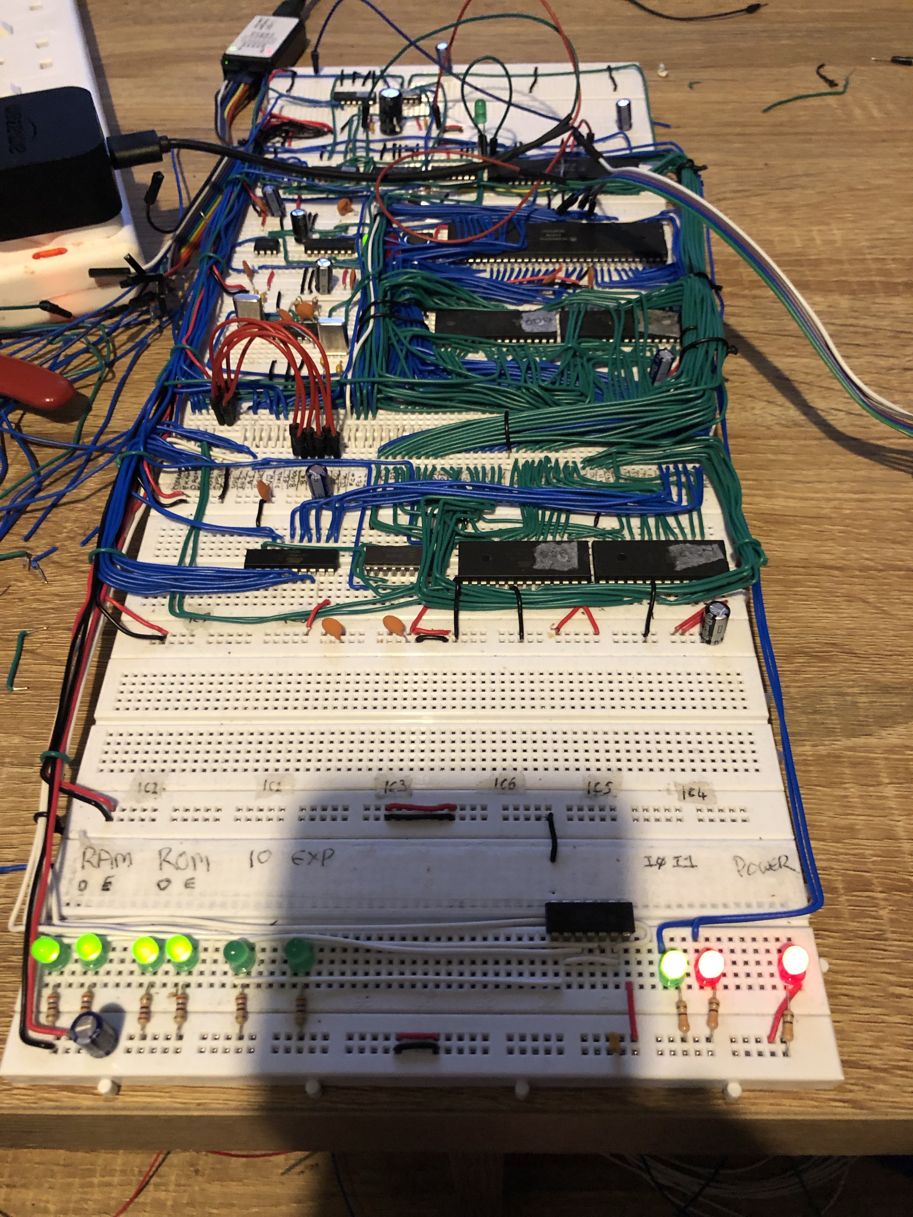
The board now looks like this:

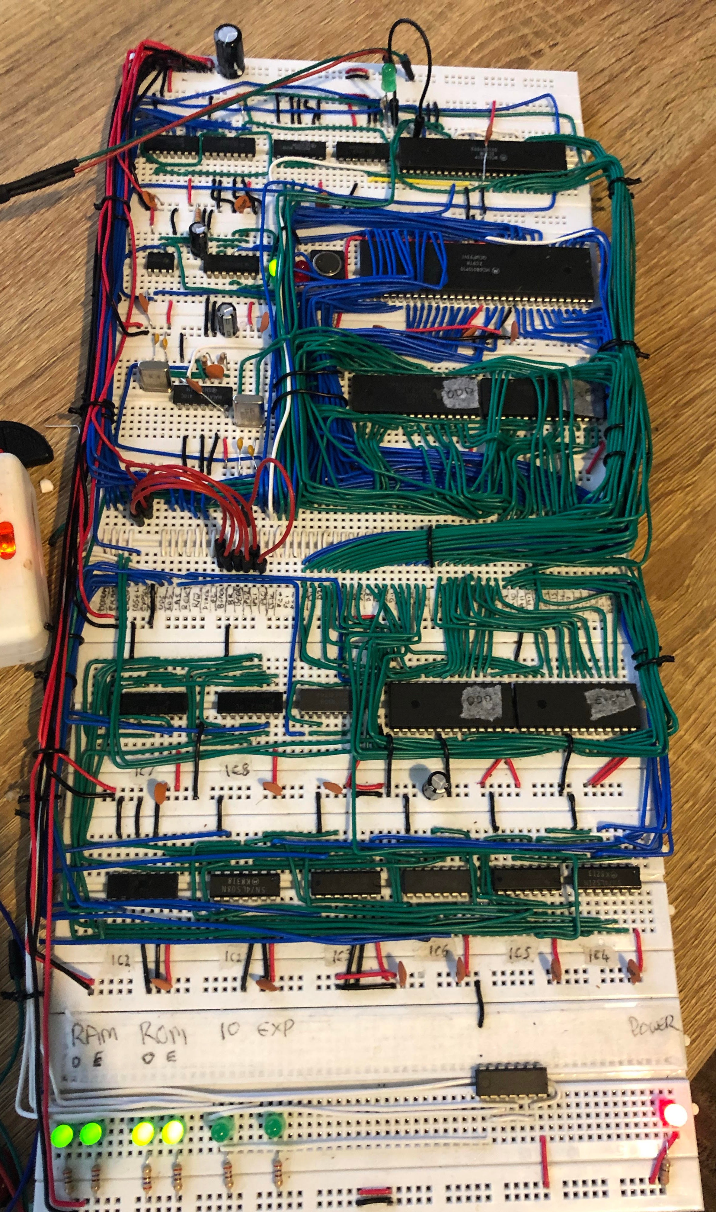
The new decoder is to the left of the ROMS. The wide open spaces to the left and below it are where the old address decoder used to live. For comparison, here's an older iteration of the board with the decoder (and it's copious wiring) still in place:

As per usual, all the code for the PLD is available (along with all the designs and code) on github.
 Ross Bamford
Discussions
Become a Hackaday.io Member
Create an account to leave a comment. Already have an account? Log In.
awesome!
Are you sure? yes | no
Thanks :)
Are you sure? yes | no
Gah. I keep thinking "it hasn't been long since Ross' last post, I should get going again" and then I see you've moved ahead in leaps and bounds :) Way ahead of me now. Unfortunately for my 68k project I bought a non-running motorbike which is sucking up most of my free time!
Are you sure? yes | no
Megabyte vs motorbike, mmm tough choice. 😉
Are you sure? yes | no
It's a '89 model bike (97 manufacture) so at least it's in-keeping with the general time period for my hobbies!
Are you sure? yes | no
I'm sure you'll get yours going again someday :) And in the meantime, you're having fun (rebuilding a bike does sound pretty awesome!) and that's all that counts :)
Are you sure? yes | no
Nice going. 👍 Maybe one day I'll draw on your work to do something with my 68k CPUs.
Are you sure? yes | no
Thanks! It was your comment on a previous log that put the idea of using a CPLD into my head :)
Are you sure? yes | no