Ross Bamford
-
Handling the /BOOT line
04/21/2019 at 20:59 • 0 comments(EDIT: This log is wrong. I was obviously not thinking properly when I wrote it. The full story is in the next log but TL;DR is that it's four memoy cycles, not four clock cycles).
As discussed in the previous log about the address decoder, I need a way to hold a /BOOT line low for the first four clock cycles after a reset. This means using some kind of counter.
I don't have any of the 7400-series counters to hand, and neither does my awesome local electronics store at the moment, but what i do happen to have is a ton of 74LS174 hex D-Flip-flops (with common reset, unlike the 72LS74). So I'm just going to add one chip and use five of the flip-flops instead.
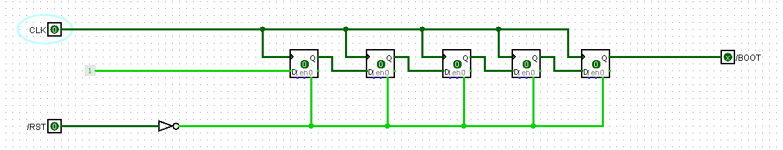
I've not even EAGLEd this yet, but the concept looks like this in Logisim (when the reset line is active):
![]()
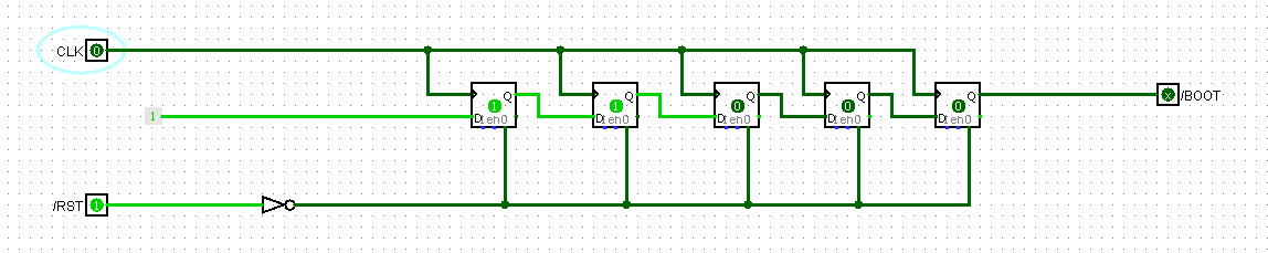
And, after reset goes high and the first couple of clocks have passed, /BOOT is still low:
![]()
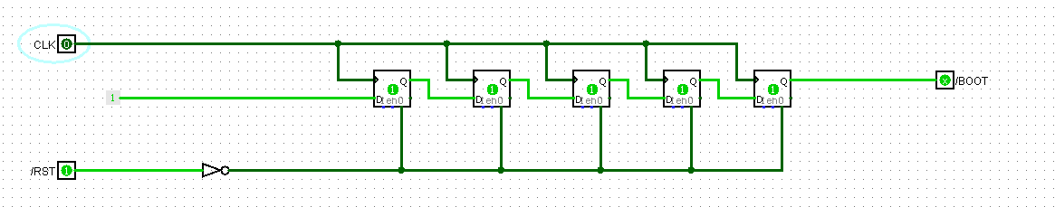
But from the fifth clock onward, /BOOT goes high, and stays high, until /RST goes low again.
![]()
This is pretty simple (it's really just a 5-bit shift-register with its input tied high) and stays with my philosophy of trying to work with what I've got, rather than reaching out for another IC that does what I need, but probably stuff I don't need, too.
Anyway, the theory's there. I'll find out if it works once the rest of the parts for the address decoder arrive and I can actually build it.
-
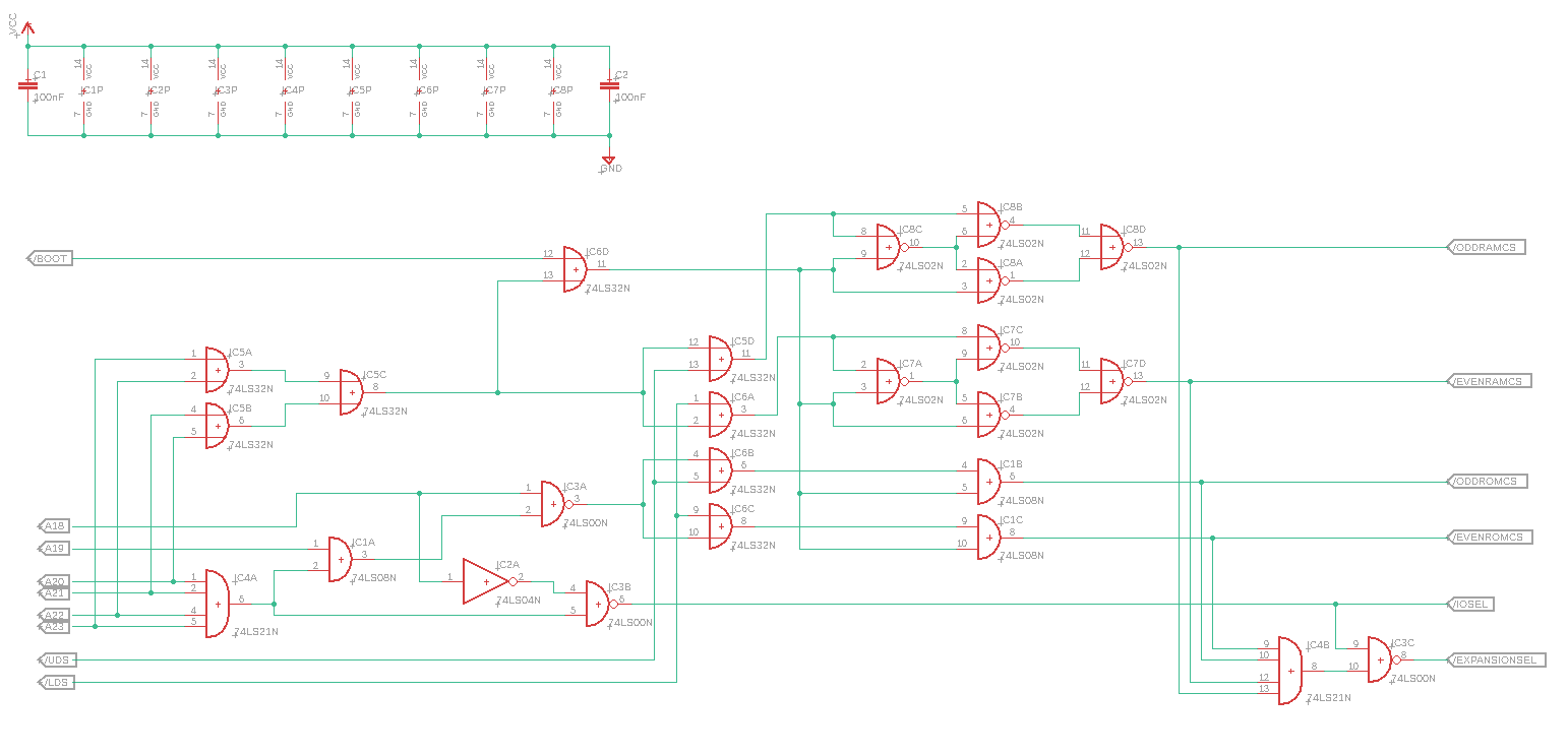
The Address Decoder
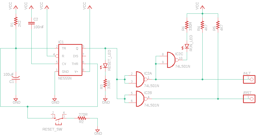
04/21/2019 at 20:34 • 2 commentsAddress decoding for the m68k is a bit more involved than for most (all?) of the 8-bit CPUs that were around at the same time, and so requires a bit more careful design. The specific things that make it complicated are:
- The larger (16MB) address space
- The different address spaces supported by the processor (e.g. Supervisor program)
- The /UDS and /LDS lines (used to select upper byte, lower byte, or both bytes for a 16-bit operation)
- The fact that there's no separate IO address space
- The requirement to have ROM at 0x00 for the first four clock cycles, then RAM there afterward
My address decoder design completely ignores the second item on that list, and just uses one address space. I may decide later to expand to support the different address spaces, but for now I don't need it.
The /UDS and /LDS lines are easily supported in the usual way for m68k builds - having odd and even ROM and RAM chips. This means that chips must always come in pairs, but it simplifies the logic quite a lot and anyway, I've found parallel chips are easier to get with 8-bit data width.
The last point is quite interesting - At startup, the m68k family expects the first eight bytes of memory to contain two 32-bit longwords, one each for the initial stack pointer and the initial program counter. Therefore, at startup (or on reset) the first eight bytes of memory should really be ROM. However, during normal execution the m68k requires RAM at the bottom of memory, to allow interrupt vectors to be modified (at least, the 68000 does. With the 68010 its not strictly necessary due to the 010 having the VBR register, but I want to have RAM at the bottom of memory in normal running anyway). The 68000 Programmers Manual does actually recommend a solution to this - simply map ROM low for the first four clock cycles. So the address decoder has to have a way to make that happen.
The memory map I decided I wanted for this system is:
- 0x000000 - 0x0FFFFF - Onboard RAM (1MB)
- 0x100000 - 0xF7FFFF - Expansion Ram (Initially, will just generate /BERR)
- 0xF80000 - 0xFBFFFF - IO (256KB)
- 0xFC0000 - 0xFFFFFF - ROM (256KB)
(With the caveat previously mentioned that, for the first four cycles after reset, ROM will be mapped low).
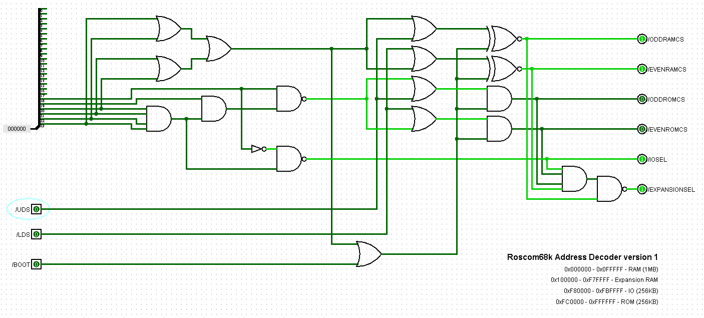
I fired up Logisim, and after a few (read: a lot of) iterations I had the following design, which I think does everything I need it to do:
![]()
The address bus is at the top left, and currently set to address 0x0. Notice the /BOOT line, which is low in the image - this is how I'm controlling whether the ROM is currently mapped low or not. You can see that, with that active, the /ROMCS lines are active.
When the /BOOT line is high (i.e. during normal running) the /RAMCS lines are active instead:
![]()
As you can see, the /BOOT line just directly selects ROM, bypassing the normal way it is selected, using the highest four address lines. This means that ROM is just shadowed low with this setup.
It also doesn't do anything with the /UDS and /LDS lines, meaning that when /BOOT is low, the chip can only do full 16-bit memory accesses - this should be fine because, according to the manual, that's all it will do during those first clock cycles, in order to read those two 32-bit values. After that point, /BOOT will go high, and the /UDS and /LDS lines are decoded as normal and used to select the appropriate chips.
The /IOSEL line indicates that the address decoded falls into the IO range - this will need further decoding to select the appropriate IO device - since I have none at this point, I'm doing nothing further with it. The same goes for the /EXPANSIONSEL line (which indicates a RAM address outside the 1MB I'll have on the board) - I might eventually use this to drive decoding on a memory expansion board, but for now I'll just tie it to /BERR on the CPU.
This is how it looks in EAGLE:
![]()
The major difference to notice is that I just haven't been able to get hold of XNOR gates in the 74LS series. There are some listed but they seem only to be available in the later HC series which isn't TTL compatible. I could probably have gotten them in HCT, but to be honest I have a bunch of 72LS02 chips so I decided to just go ahead and build the XNORs with NOR gates. It ups the chip count by one, but to be honest I was tired of trying to source the chips and wanted to just go with what I had.
That said, this still isn't built yet because I'm waiting on a couple of chips (a 74LS32 and a 74LS00) but they should be here in a few days, so I'll update once its built.
The one thing left to do is handle that /BOOT line, which I'll write up in the next log.
-
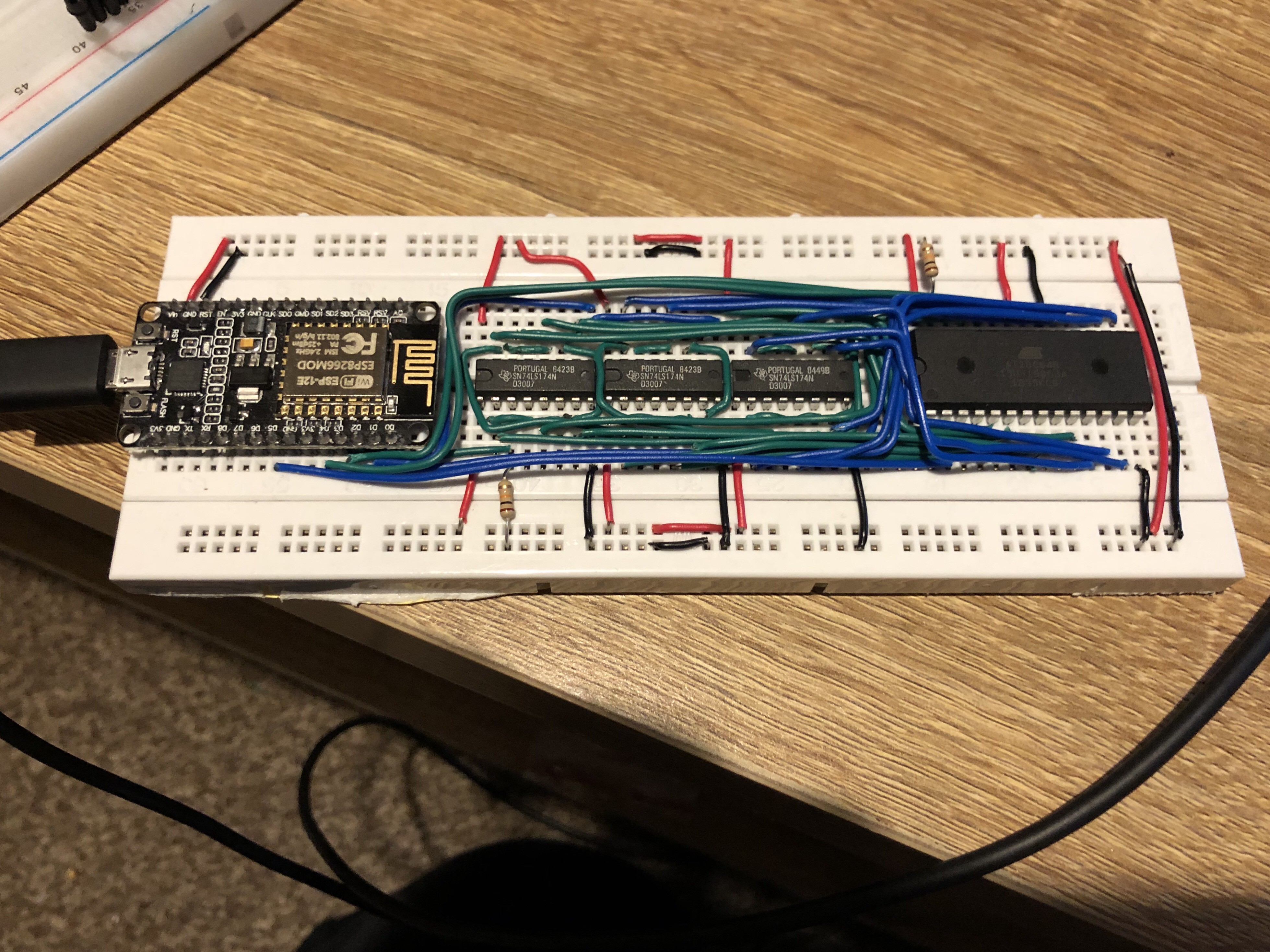
A very hacky EEPROM programmer
04/13/2019 at 13:15 • 3 commentsI know I literally just said that the next log would be about the address decoder, but then I remembered I've been meaning to write a quick log about the EEPROM programmer I hacked together for the m68k project, so here's that instead.
(TL;DR - It's on Github: https://github.com/roscopeco/eeprom-programmer)
Once the address decoder is built, I'm obviously going to need to program the EEPROMS for the m68k build. I could go the easy route and just buy one, but I decided I had enough stuff lying around that I should be able to hack one together. It turns out I did, but I had to make some, ahem, compromises to make it work.
Quoted from the README on Github:
This project uses an ESP8266 dev board (NodeMCU 1.0) along with three 74LS174 hex D-flip flops to program the 64 Kbit EEPROMs I'm using in my m68k breadboard computer. The choice of components may seem a bit odd - the design was driven entirely by what I had available on the bench at the time, and my being too impatient to wait for a ten-quid programmer to arrive in the post. So I just hacked this together quickly to tide me over.
So basically I just built a shift register driven by the NodeMCU and then used some of the spare GPIOs to drive the W/E line on the ROM. Obviously I could have used shift registers instead of the flip-flops, but I didn't have any.
I'll say no more about it here, it's well documented on Github and the code is there too. So I'll just post a picture of it and move on to address decoding (for real, this time).
![]()
-
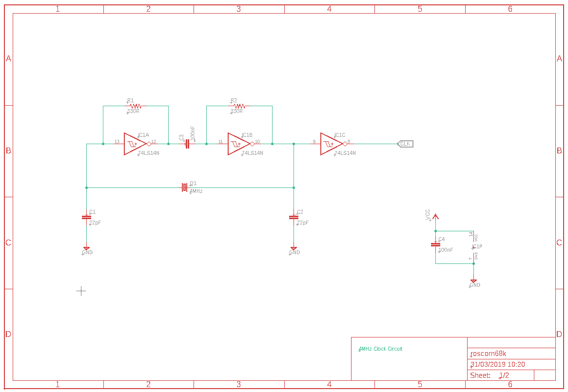
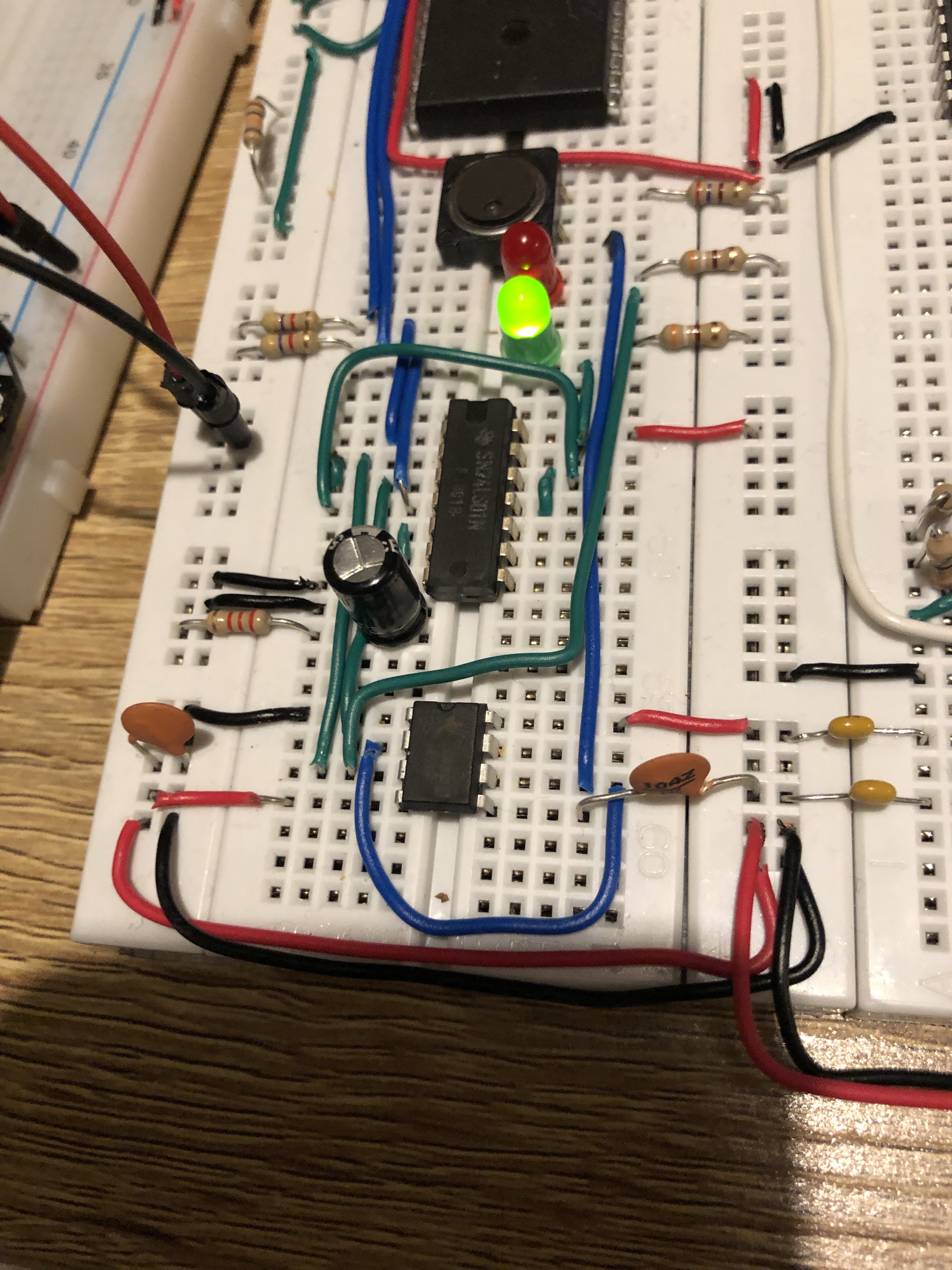
The Clock Circuit
04/13/2019 at 12:44 • 0 commentsFor the 4MHz clock circuit on the m68k build, I'm using a simple circuit based on a 4MHz crystal, a few capacitors and resistors, and three Schmitt trigger inverters on a 74LS14.
Looking around the Internet for a suitable circuit didn't really turn up anything I could directly use, but it did turn up a ton of information on the theory of these things (some of which I still don't understand!). This was a Good Thing(tm) as it meant I had to actually figure out how to build a clock circuit for myself, rather than just copying someone elses!
The design I ended up with looks like this:
![]()
(I know, the names and values should all be the same orientation - I'm getting better with EAGLE but still no pro!)
In hindsight, this is probably more complicated than it needs to be, but it does work. I've also read that it might be a bad idea to use Schmitt trigger inverters for the first two gates in the circuit, as they might fail to oscillate, or oscillate at an unintended frequency, due to the Schmitt triggers making a non-linear amplifier. It works well right now on breadboard but I guess I might need to revisit if I ever build a PCB for this, or when I up the frequency to the 10MHz the m68k is rated for.
Obviously this is my first real attempt at working with a crystal and trying to make a stable oscillator, other than just following someone else's design, and I'm sure it's both non-optimal and not really correct. That's part of the reason the reset circuit holds the reset line high for a relatively long time at power-up (~2M cycles) - to give this thing lots and lots of (read: far too much) time to become stable.
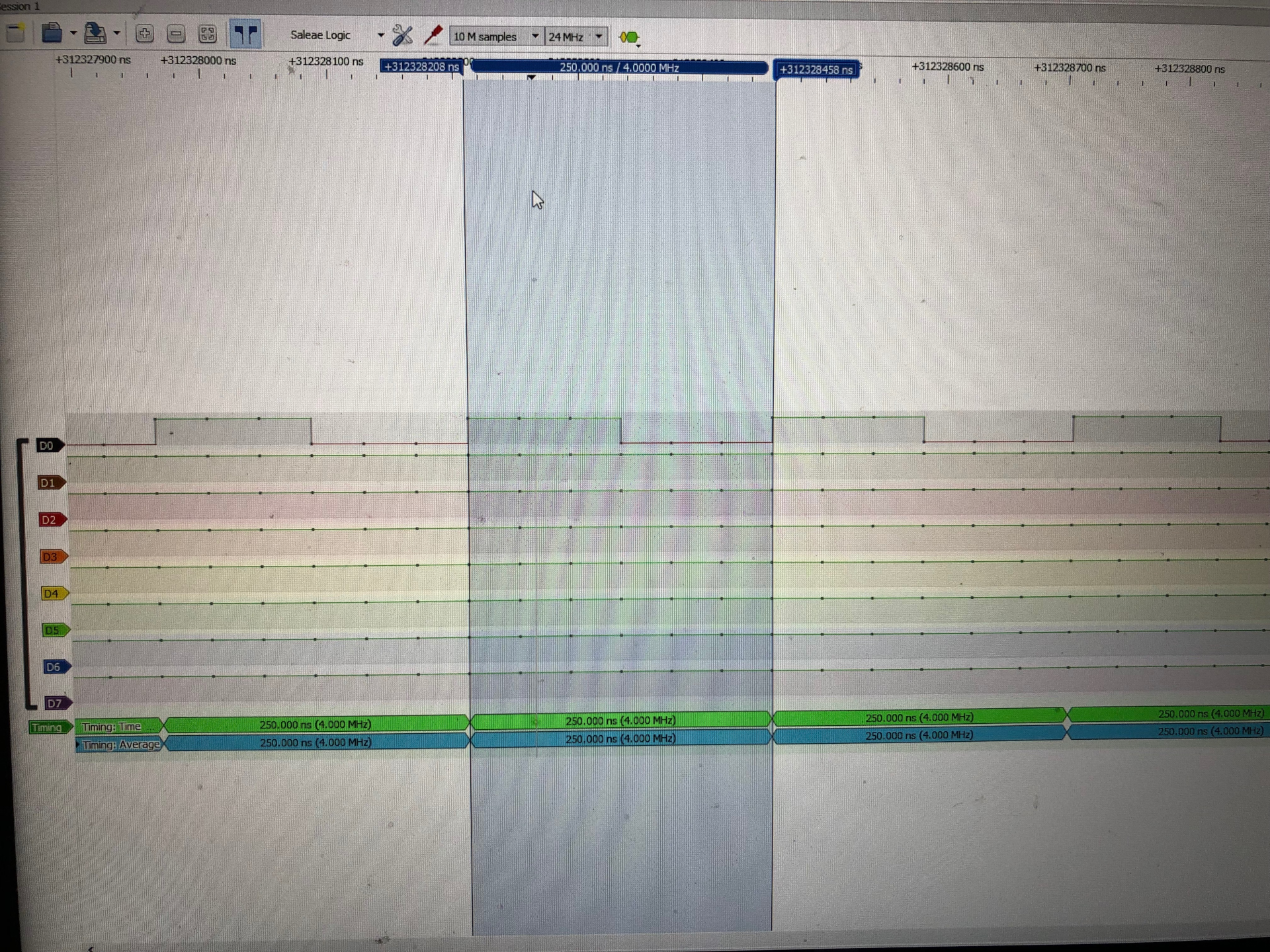
This circuit was easily the most difficult thing I've faced so far with the m68k build, but the satisfaction when it worked and gave a solid 4MHz clock on the logic probe was immense :). Even better was when I left the chip free-running overnight and came back in the morning to find it still happily blinking lights on the top eight address lines.
Here's a shot from the logic probe showing the clock signal:
![]()
(Yes, I wish I'd cleaned my screen before taking that).
And here's the built circuit on the breadboard:
![]()
The next log will be the address decoder, which is designed but not yet built as I'm lacking a few 7400-series ICs it needs.
-
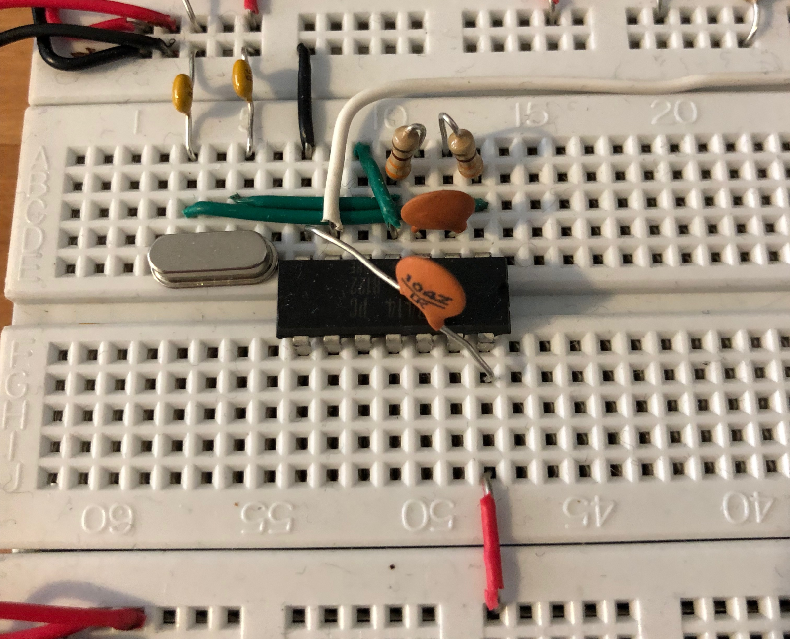
The Reset Circuit
03/17/2019 at 22:18 • 0 commentsHandling Reset with the m68K is a little bit involved, and every project seems to handle it in a slightly different way. This log represents the way I've approached it, and it seems to work (right now, that means it successfully gets the processor free-running, has some status LEDs, and when the reset button is pushed it resets the free-run to the bottom of the address-space).
The reset circuit has the following requirements:
- At power-on, the m68k requires us to pull the /HALT and /RESET pins low for a bit.
- It would be useful to have some LEDs showing the status of the reset and whether the CPU is halted.
- Push-button reset is needed so we can, err, push a button to reset the thing.
So basically, I need a circuit that will pull two lines low for a short period at power-on, and additionally allows me to push a button at any point to do the same thing.
This is made slightly more complicated by the fact that the two lines I need to pull low can also be pulled low by the chip itself, to signal to the outside world that a soft-reset has happened, or that the CPU is halted. Just driving the lines high when I want to deassert them isn't going to work here. I'm going to need to drive them with open-collector outputs, and weakly pull them high when I'm not driving them low.
I could tie these two lines together (see http://www.easy68k.com/paulrsm/dg/dg06.htm for example), but if I do that I'm hardwiring the CPU to reset when it halts, which for now wouldn't be an issue, but later on I'll probably want that to not be a thing.
With all that in mind, I put together the following circuit to take care of the /HALT and /RESET lines:
![]()
(Caveat: I'm still learning here and am an EAGLE noob, so shout up if I've done anything stupid!)
This is a simple delay-before-turn-off 555 circuit hooked up to the /HALT and /RESET lines via 7400 series open-collector inverters (actually NANDs with the inputs tied together in my case, but only because my awesome local electronics store, https://www.rfpotts.com/, happened to be out of stock of the 74LS05 this weekend).
For the sake of my sanity, and blinkenlights of course, it also has a RESET_LED (in red on my board) that shows when a reset is in progress. This is just driven from the output of the 555. There's also a (green) RUN_LED that is lit when the HALT line is high. I probably could have driven that directly off the line, but I decided to use one of the (otherwise wasted) gates on the 74LS01 to drive it instead.
Both /RESET and /HALT are held low for about half a second at both power-up and on the reset button push. This is way longer than is strictly necessary (about 2M clocks with my current 4MHz clock!) but it gives everything (power supply and clock) plenty of time to stabilise and is hardly noticeable in person-time so I'm not too concerned about it. If I wanted to make it shorter, I could just play around with the values of R1 and C1 until I was happy.
So that's it for the reset circuit. I have a working reset without having the two lines tied together, and the CPU seems happy with it. Next time, I'll show the clock circuit, and then we can get onto talking about the 68k itself :)
(For completeness, here's the circuit on breadboard):
![]()
rosco_m68k
A full-featured Motorola 68k retro computer, starring a 68010 running at 10MHz