-
Schematics: USB
05/17/2019 at 06:48 • 0 commentsIn the FunKey device, the USB interface has 2 purposes:
- provide an external power supply source for both powering the device and charging the built-in LiPo battery
- provide a data interface to transfer firmware upgrades, configuration files, game emulators and game ROMs
The first purpose only requires the +5V USB power and GND pins. The second purpose requires to wire the additional differential data lines D+ and D-. As we only need to operate as an USB device and although the V3s is able to work as either an USB host or USB device using the USB OTG protocol, we don't need the ID pin to determine by the cable wiring which role we must take.
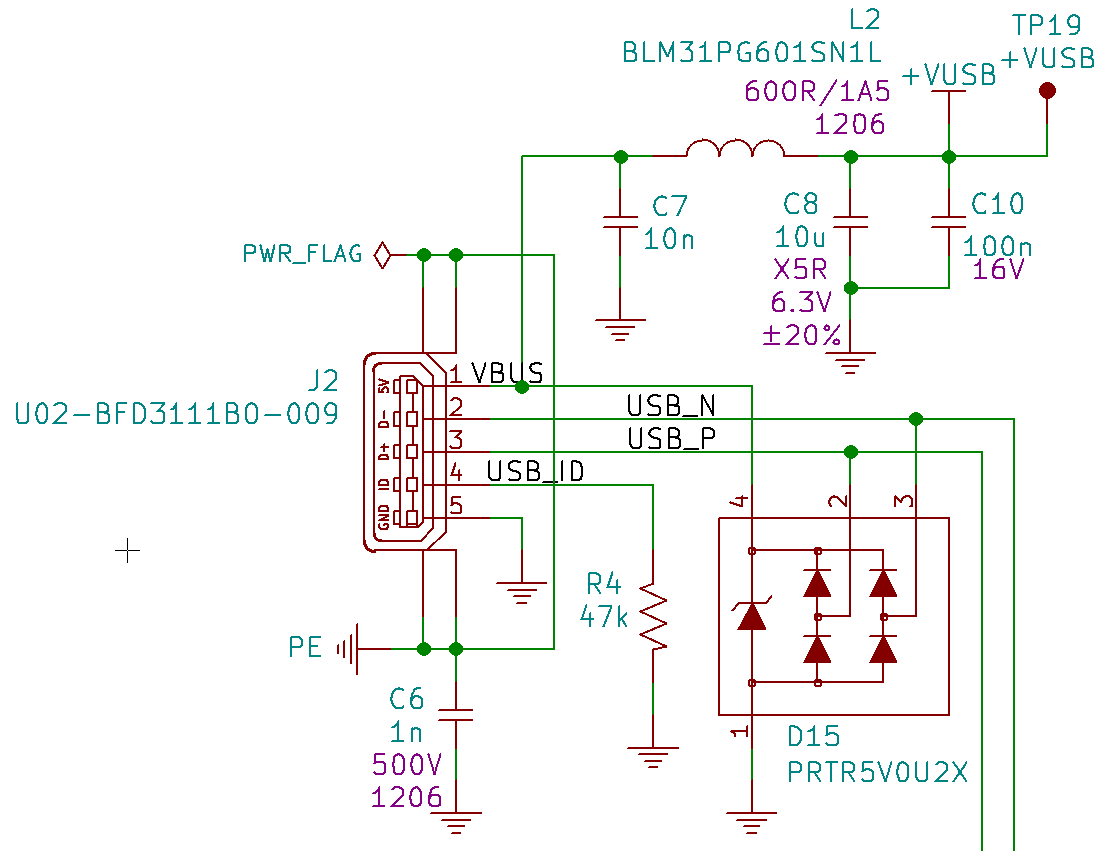
The USB schematic is the following:
![]()
Before connecting 2 devices using an USB cable, they may be at completely different absolute voltages, and during cable insertion, the shield will be in contact before the other pins, including GND. The C6 capacitor between the Protective Earth (Shield) and GND is here to provide an AC path for sinking this difference in voltage and align the GND levels when plugin the cable.
The resistor R4 on the USB ID connector pin should probably not be mounted: as we act only as an USB device, this pin should be left floating.
The capacitors C7, C8, C10 and ferrite bead L2 form a constant-k 3 pole CLC low pass filter to remove any spurious in/out on the USB power supply wire. The USB 2.0 specification limits the maximum bulk capacitance value to 10 µF in order to avoid power supply excessive droops when plugin in a device with a discharged large bulk capacitor.
D15 is a combined TVS protection diode for the VBUS pin and a set of clamping diodes that will limit the voltage on D+ and D- pins to stay between GND and VBUS levels to in order to protect the V3s USB driver from under / over-voltages.
-
Schematics: Audio
05/12/2019 at 19:24 • 1 commentPlaying audio is absolutely part of the gaming experience!
So for a retro gaming console like the FunKey, we need to have a decent audio playback, despite its lilliputian size.
By decency, we discarded the solution using a piezo-electric buzzer: these can get a loud sound in a small volume, but only at their resonance frequency, so the sound quality is extremely poor.
Turning back to the solutions used in modern smartphones as an example, there are 2 paths to consider:
- playing audio internally by the mean of speaker(s)
- playing audio externally by using headphones, with or without a cord
The speakers used in today's smartphones are rather sophisticated and achieve very good performance. However, these are using made-to-measure speakers and cavities, such that they cannot be found and reused as standard parts in a design like ours.
As for the external audio solution, we have a problem: the FunKey is so small that it is not possible to integrate an audio jack to connect headphones! And despite our search, there is no simple and small enough way to use Bluetooth to output audio to cordless headphones either.
The best solution we have found consists in using a single tiny speaker from CUI CDM-10008, that is able to output 72 dB spl @ 1m from a 0.3W input power, with relatively modest dimensions: 10 mm diameter and only a 2.9 mm thickness.
Connections are not easy though, since this speaker is meant to have wires soldered to its pads, but we are trying to convert it into an SMT device in order to gain space in our small enclosure! We don't have a satisfying solution yet that is possible to use for mass production, we are still working on it!
Schematic
The resulting schematic is simple, as the Allwinner V3s already contains an analog stereo audio codec (coder/decoder): we only have to take one of its headphone output channel (left or right) and feed it to a mono audio amplifier.
We chose the PAM8301 chip because of its cheap price, good availability, its more than sufficient output power of 1.5W and its filterless operation, meaning that no bulky series capacitor is required to drive the speaker.
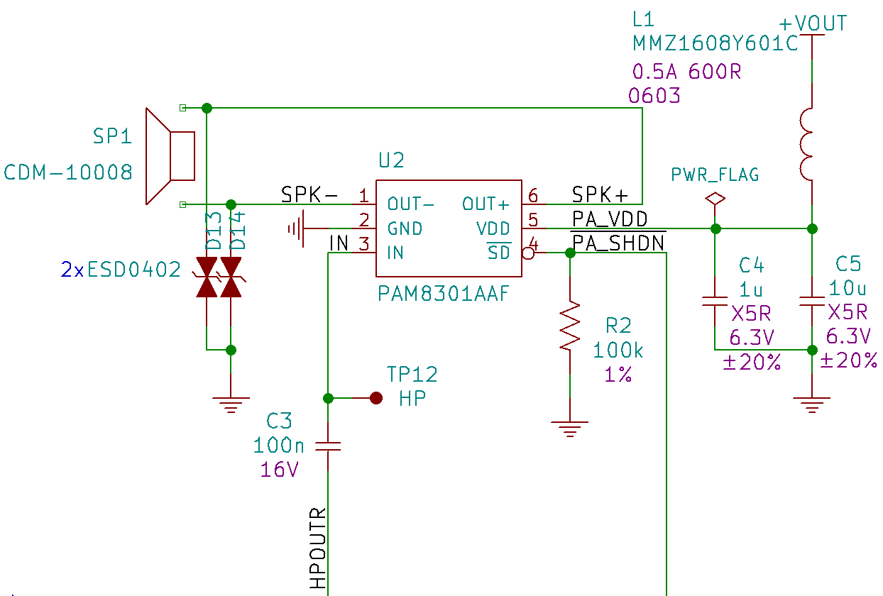
Here is the corresponding schematic:
![]()
We chose the right headphone channel HPOUTR that is fed to the audio amplifier U2 through a DC-bias filter capacitor C3.
The audio amplifier /SD shutdown input is driven by one V3s GPIO, with a pull-down resistor R2 to disable the amplifier by default.
The audio amplifier power supply is filtered using a ferrite bead L1 in order to eliminate high-frequency digital noise, and decoupled by 2 capacitors C4 and C5, as recommended in the device datasheet.
The speaker SP1 is driven in differential mode in order to get the maximum voltage swing and thus the maximum power available for a given output current.
Two ESD protection TVS diodes D13 and D14 are added, since the speaker may be accessible to the user through the enclosure grid in front of the speaker.
-
Schematics: Buttons
05/07/2019 at 20:39 • 0 commentsAs a generic game console emulating many classic ones, the FunKey requires numerous buttons:
- A soft "ON/OFF" button
- A "+" control pad with "Up", "Down", "Left" and "Right" buttons
- A "x" control pad with "A", "B", "X" and "Y" buttons
- "Start" and a "Select" buttons
- L and R shoulder buttons
As we have sen in the log on the PMIC, the soft "ON/OFF" button is directly connected to the power management chip, so we are left with 4 + 4 + 2 = 12 buttons for game control.
GPIO Requirements
The Allwinner v3s CPU comes in a large 128-pin TQFP package, with a lot of exposed (51!) GPIO pins:
- PB0 to PB9 (10)
- PC0 to PC3 (4)
- PE0 to PE24 (25)
- PF0 to PF5 (6)
- PG0 to PG5 (6)
The FunKey specializes some of them for specific interfaces like SDCard, PWM, SPI and I2C buses, console UART, but most of them are left available for I/Os.
Button Interrupts
However, in order to detect when the buttons are pressed / released efficiently, the best solution is for them to generate an IRQ (Interrupt ReQuest) to warn the CPU that the corresponding button state has changed, instead of using an inefficient regular polling method.
Unfortunately in the V3s, only PB0 to PB9 and PG0 to PG5 support this GPIO IRQ capability. Worse, most of the pins PB0 to PB9 are already used for UART, I2C or PWM functions.
It is possible to route these functions to different pins and recover enough IRQ-capable GPIO pins: this is what we did for our #Funkey Zero project.
GPIO Expander
But for the FunKey device and given the small PCB size, this solution puts a lot of constraints on the PCB routing, at such a point that we decided to use a dedicated I2C GPIO expander chip to relieve the burden from the main V3s CPU.
A common chip for this purpose, that is well supported in the Linux kernel is NXP's PCAL6416AHF.128. It is marketed as a "low-voltage translating 16-bit I2C-bus/SMBus I/O expander with interrupt output, reset, and configuration registers": it just matches exactly what we need!
The connection with the V3s CPU is achieved using standard I2C clock (SCL) and data (SDA) signals, plus an additional IRQ signal driven by the I/O expander when pre-programmed conditions are met, such as a key press / release event. A RESET signal driven by the PMIC PWR_GOOD output is used to initialize the chip when required.
Schematics
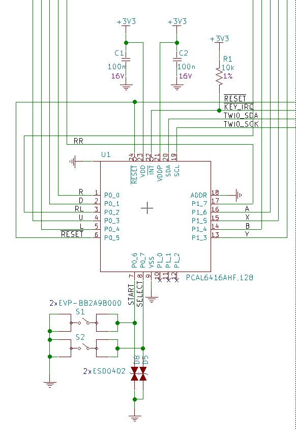
Here is the corresponding main schematic for the buttons:
![]()
The main component is of course the I/O expander U1, with the control signals to the CPU/PMIC on the east side.
The chip's /INT signal is pulled up to the +3V3 power supply by the resistor R1, such that the active-low interrupt signal is disabled by default.
The I/O expander chip features 2 separate power supplies VDD and VDDP for the core and peripheral respectively, each decoupled by a bulk capacitor C1 and C2.
Except for the GPIO I/Os, the only remaining pin is the ADDR pin 18 which provides the I2C address LSB bit, so that you can address 2 PCAL6416AHF.128 chips on the same I2C bus by wiring this pin differently.
One oddity is that the pin 6 (P0_5) is connected to the /RESET signal: it is a routing trick to get this signal to go through this pin pad, as it was very difficult to access it otherwise...
The "Start" and "Select" buttons S1 and S2 are 2 low-profile SMT tactile switches, each featuring an ESD protection TVS diode D8 and D5, as these buttons are of course accessible by the user!
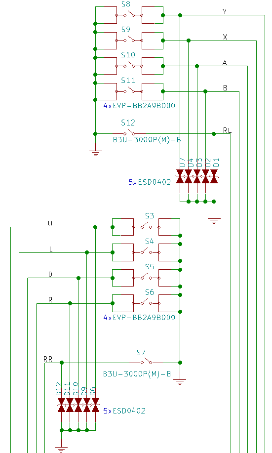
The other buttons are wired in the same fashion:
![]()
The "U", "L", "D", "R", "A", "B", "X" and "Y" buttons S3, S4, S5, S6, S8, S9, S10 and S11 are of the same kind and also have a respective TVS diodes D2, D3, D4, D5, D6, D7, D8, D9, D10 and D11.
The left (S12) and right (S7) shoulder buttons are right angle SMT tactile buttons, with their TVS diode D1 and D12.
Benefit
The main advantage of this solutions is that the 12 signals to wire the buttons to the CPU are replaced by only 4 signals, from which 3 are shared with the other I2C peripherals (the PMIC) on the bus.
It is then much easier to route this dense PCB by delegating the button GPIO handling to a satellite chip.
-
Schematics: Console
05/04/2019 at 20:34 • 0 commentsThe Allwinner V3s provides 3x UARTs (UnAsynchronous Receivers / Transmitters): UART0 with only RX and TX signals, and UART1 and UART2with additional RTS and CTS flow control signals.
As almost all SoCs, tha Allwinner V3s provides a serial console as a control terminal for debug or normal operation. By default, it is mapped to UART0, and it is used by the BROM (Boot Rom), the U-Boot bootloader and by the Linux kernel to output messages during the boot process, and later by the Linux kernel to log messages during normal operation. Depending on the configuration, it can be used too for loging into the system over an UART.
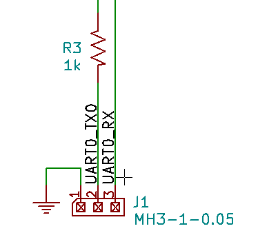
The Console schematic only requires a minimum of external components:
![]()
Besides the 3-pin 1.27 mm (0.05") pitch header J1 that will not be mounted on standard products, there is only a single series resistor R3.
What is the purpose of this resistor?
- As explained previously for the SD Card clock signal, this may be to prevent ringing. But given the relatively slow signal speed (115200 bps), it is not the case here
- If it were placed on the RX input signal, this could prevent frying the input pin if a large voltage (+5V, for example) is applied to it by dissipating the excessive voltage as heat in the resistor. It is not the case here, since the resistor is on the TX output signal, but we could have one added, if only we had some space left on the board...
- In fact, the resistor is on the output TX signal to prevent short-circuits if the serial cable is reversed and the 2 TX outputs are connected together, one driving the signal low, while the other is driving it high: again in this case, the voltage difference between the 2 outputs will be burned as heat in the resistor, saving the output buffers!
Note that there is no ESD protection TVS diodes: this interface is not supposed to be mounted in the final user device, and PCB space is really constrained in this area, so they are omitted.
-
3D Printed prototypes before injection molding
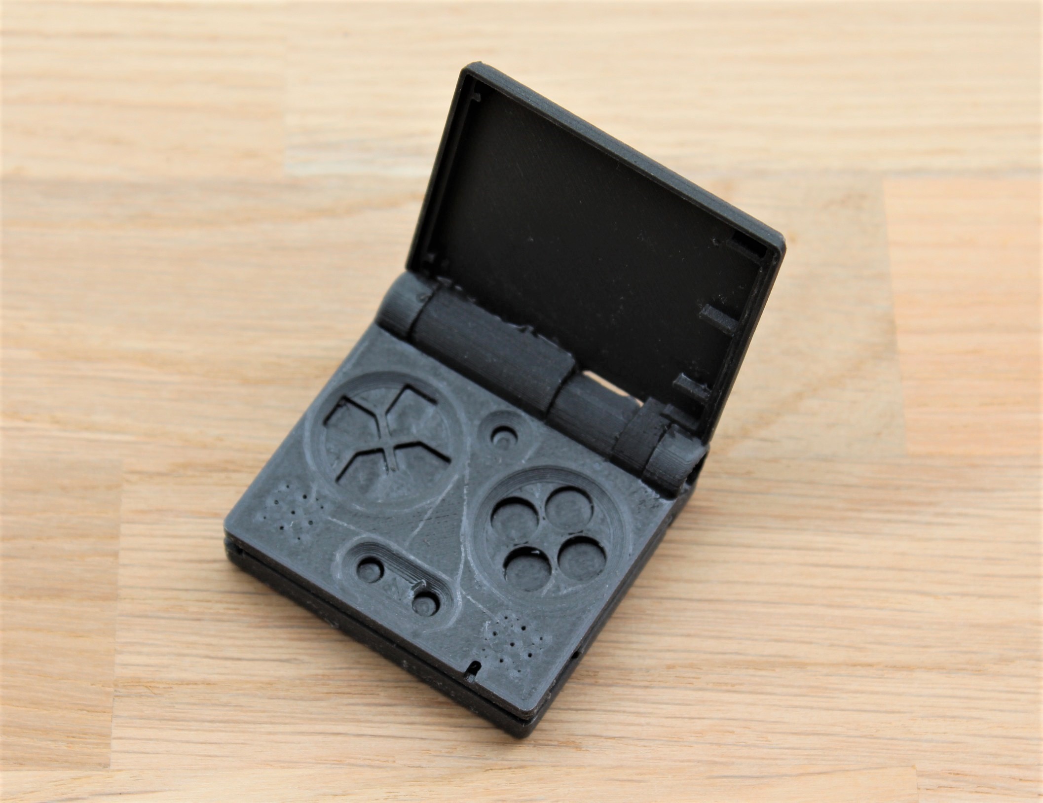
05/01/2019 at 20:17 • 2 comments![]()
Introduction
FunKey's design has been completely rethought. It is now sturdier, slimmer, with an active hinge that puts no stress on the cables and most importantly thought for production. We have designed every component while thinking about the injection molding process, this means clearance angles, drawers for the mold and other things that will be explained in a dedicated log about the design.
Here instead we would like to take an unconventional path and start talking about the in-between process that is after the design and before the injection. Let's say your design for injection molding parts is done, how do you test it to assert its validity before investing thousands of dollars in a mold and go into production?
Nowadays, we are lucky to live in a world where 3D printing not only exists but has been vastly democratized to the masses. Just between our three group members we own about five different 3D printers (not all in the best of shapes but they still help making the point). In order to validate our design, then 3D printing is the right solution, but FunKey being what it is - that is to say very tiny - not all 3D printing technologies are adapted to our needs.
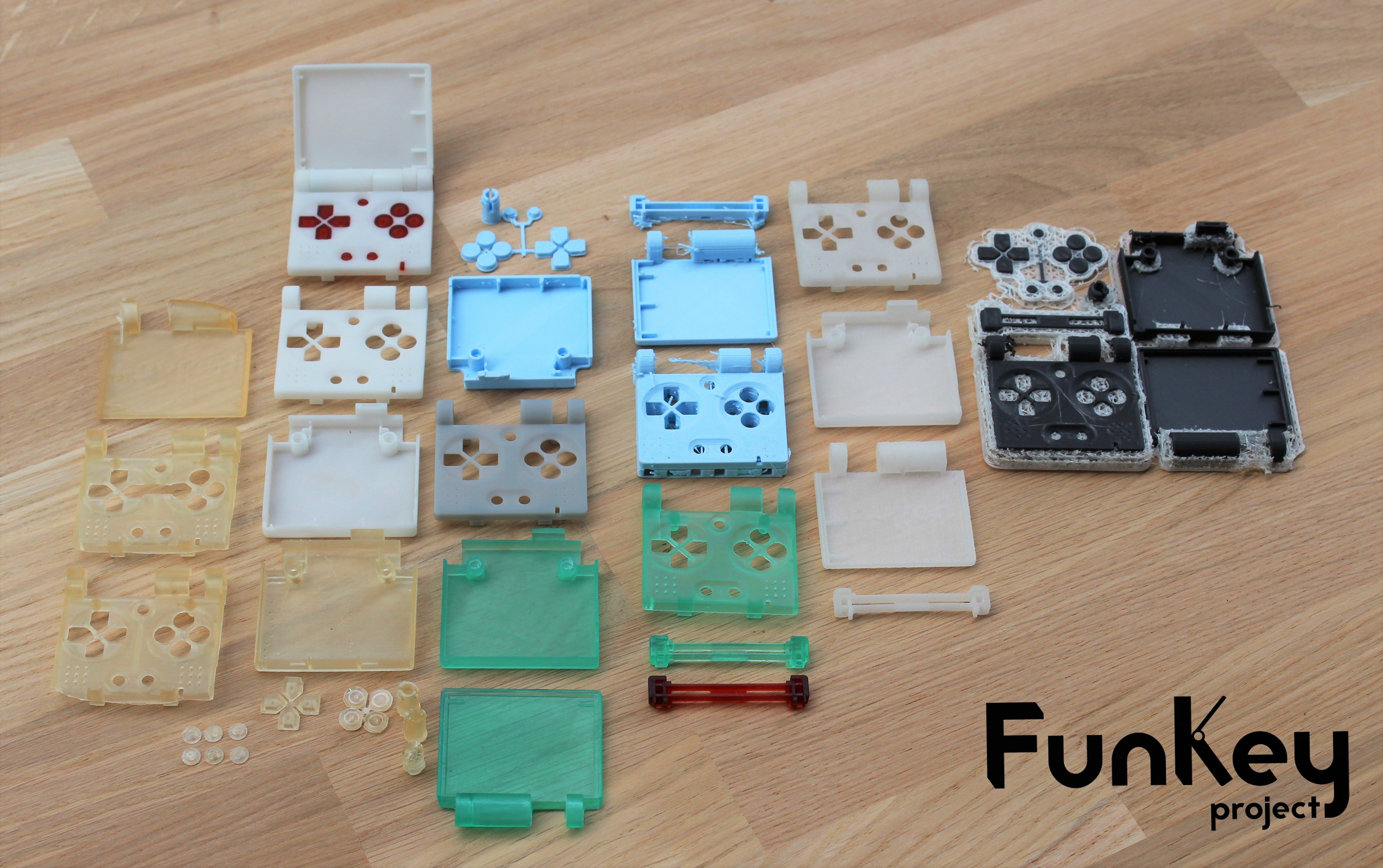
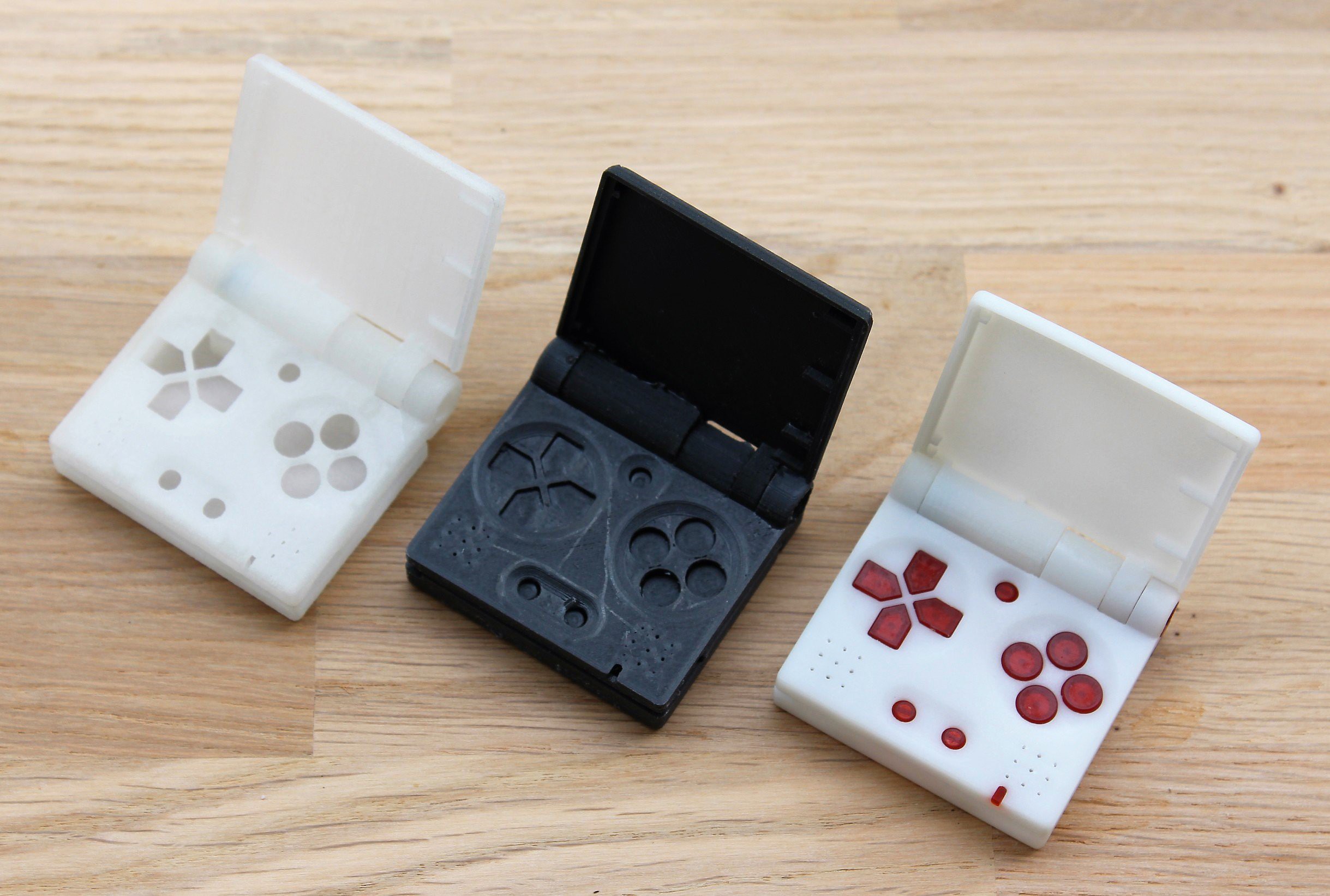
The question is, then, which type of 3D printing technology is the most adapted to our needs? We have tested the three principal ones: FDM, SLA and SLS and wanted to report our results in this log so that other makers can use this knowledge.
Brief description of the different 3D printing technologies we used
- FDM (Fused deposition modeling) which consists in building parts layer-by-layer from the bottom up by heating and extruding plastic filaments. It is by far the most common technology among hobbyists since great quality printers are now available for a few hundred dollards and the filament is relatively cheap ().
- SLS (Selective laser sintering) which sinters a powder by using a laser. Thiese printers are still way too expensive to be accessible to the mass market but it is possible to contract 3D printing companies to get prints for an affordable price.
- SLA (Stereolithography) and/or DLP (Direct Light Processing) which solidifies a liquid resin layer-by-layer by photopolymerisation. Formlabs has democratized this technology which was previously reserved to professionals (even if the printers are still relatively expensive compared to FDM ones as well as the material).
Comparison of the print results
The mechanical properties to consider for our prototype are the following:
- resistance
- precision
- surface finish
For the FunKey, we need a great precision for all the small details, a good surface finish and a sturdy case to resist the efforts on the hinge.
FDM
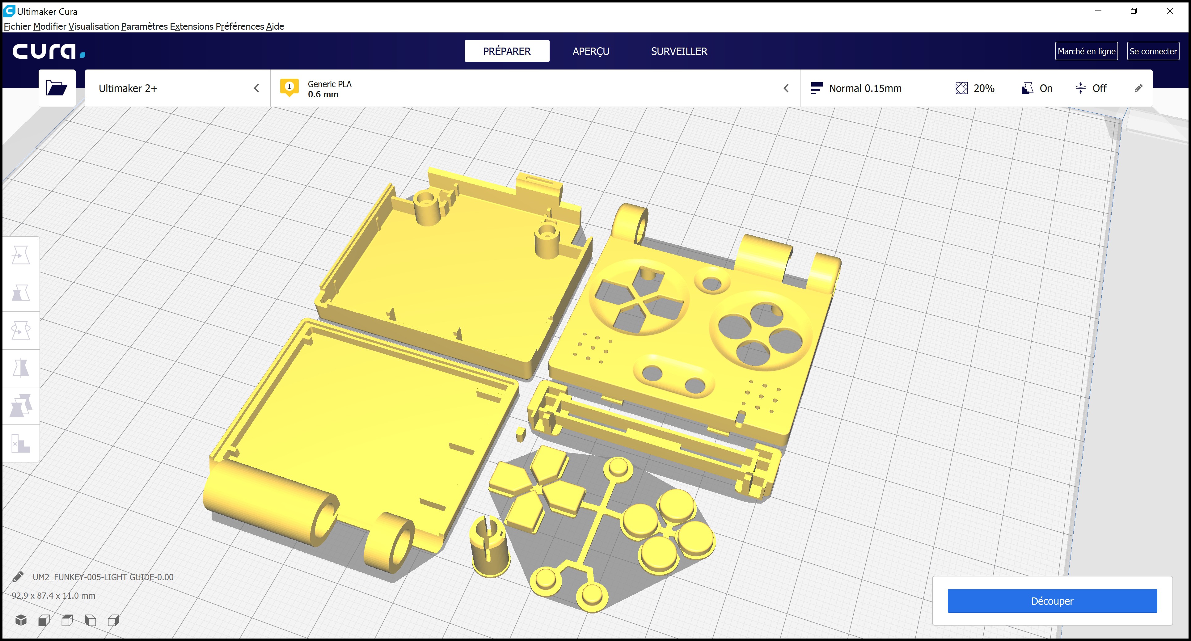
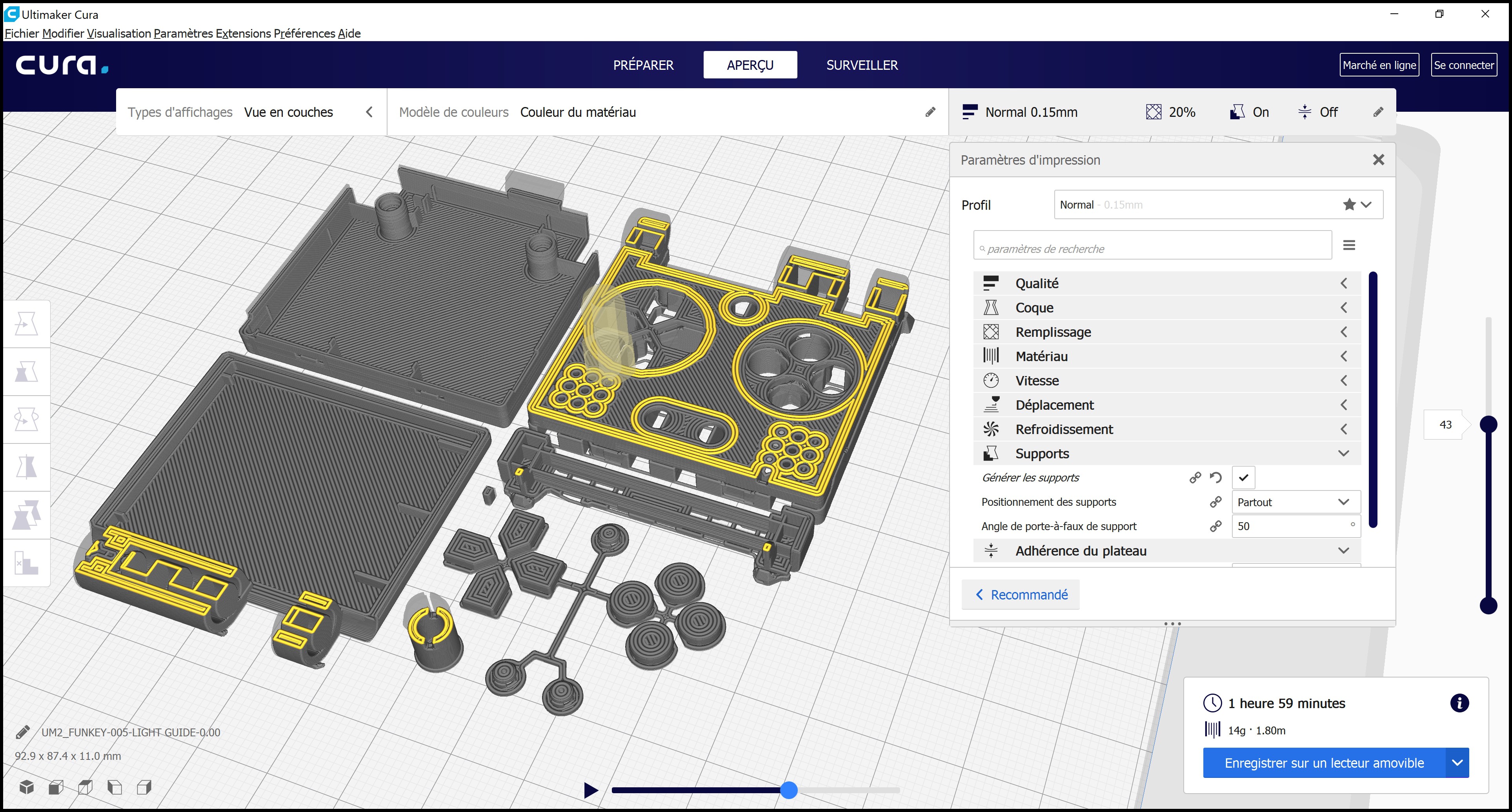
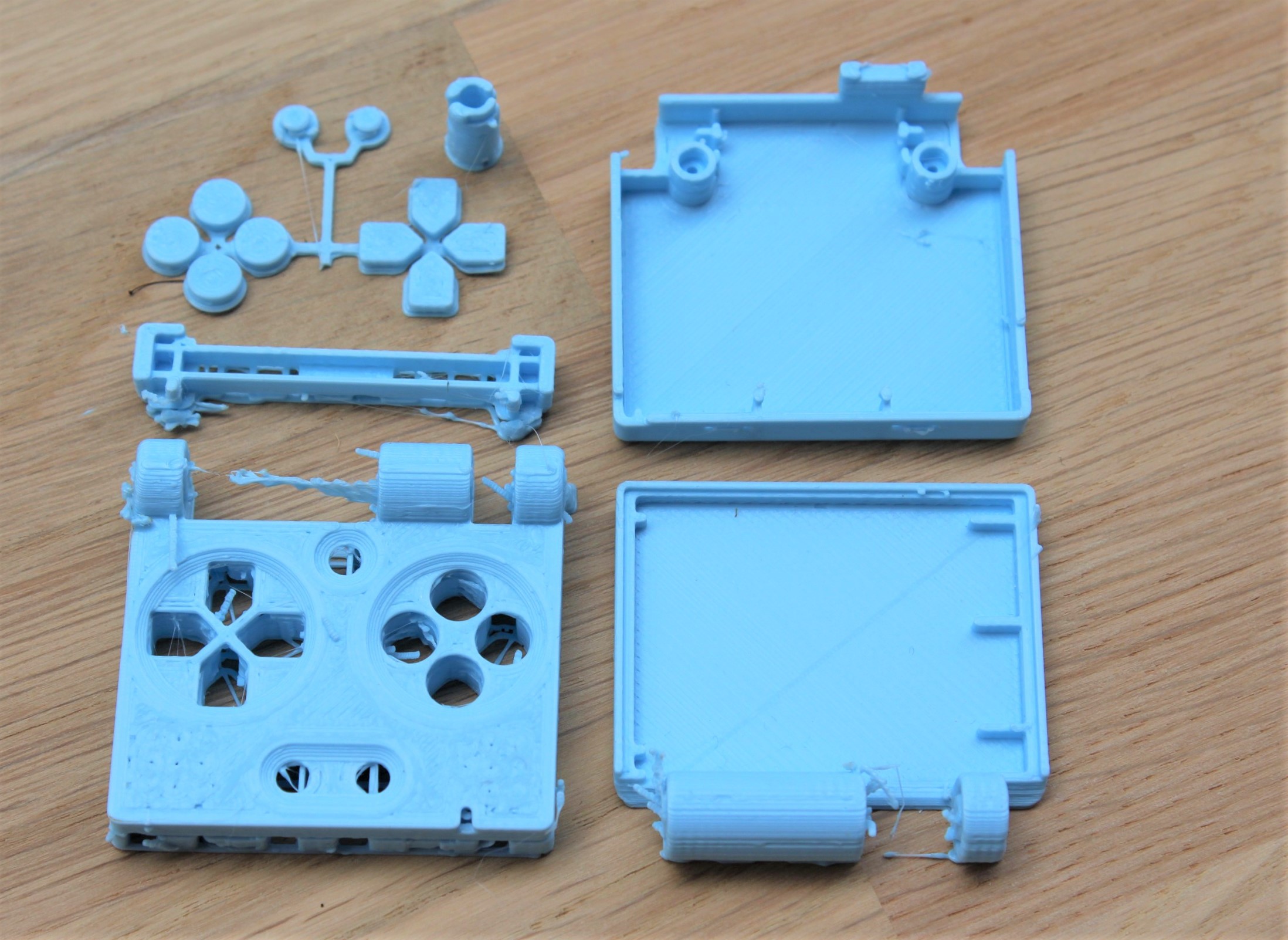
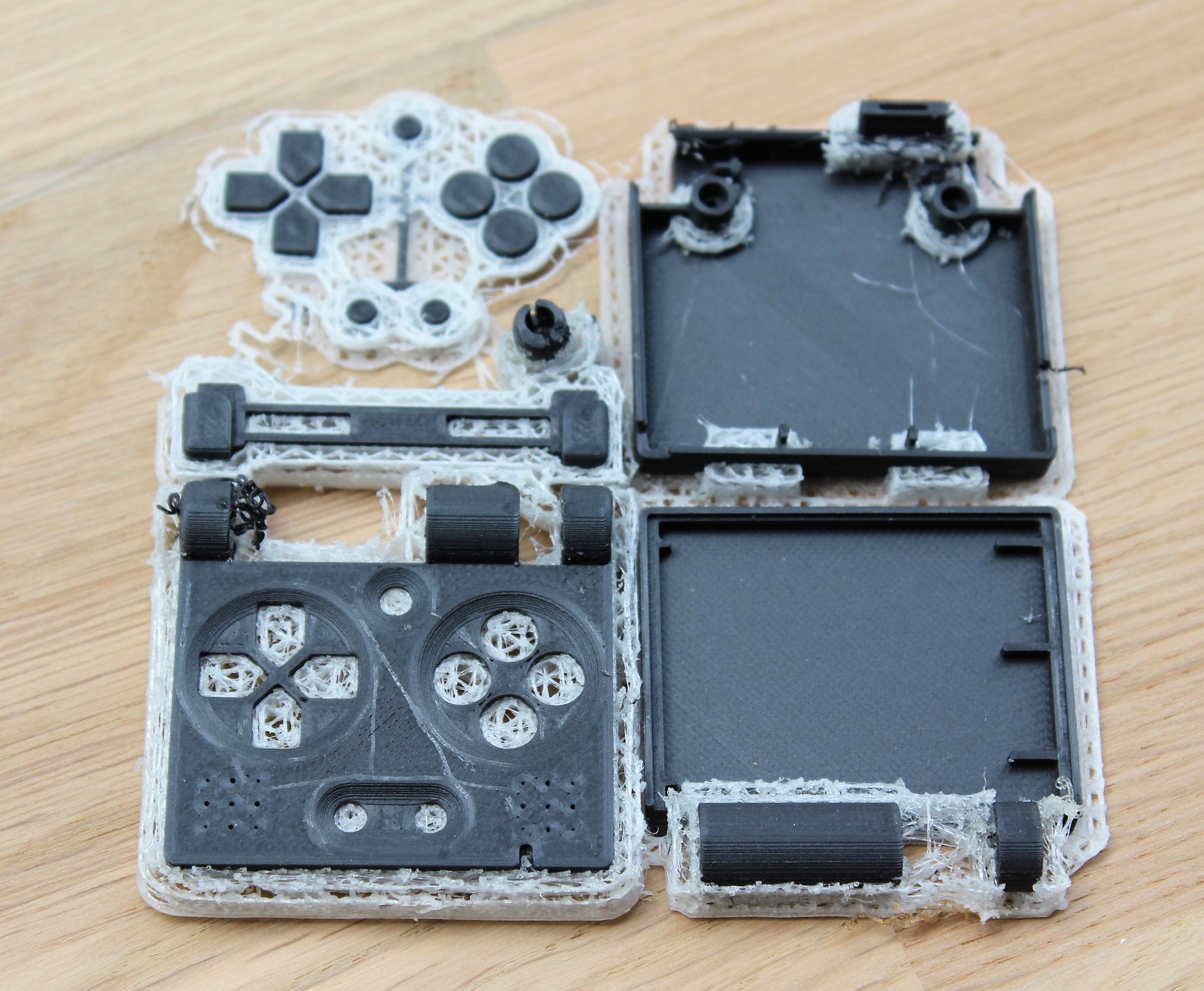
For this technology we have tried two prototypes, one printed with a common simple extrusion printer and the other with a double extrusion printer with a water-soluble material. The water-soluble material is used as support material and life-changing during the post processing of prints. You can see below the prints realised with an Ultimaker 2+, nozzle 0.6mm, layer height 0.15mm and PLA filament.
![]()
![]()
![]()
![]()
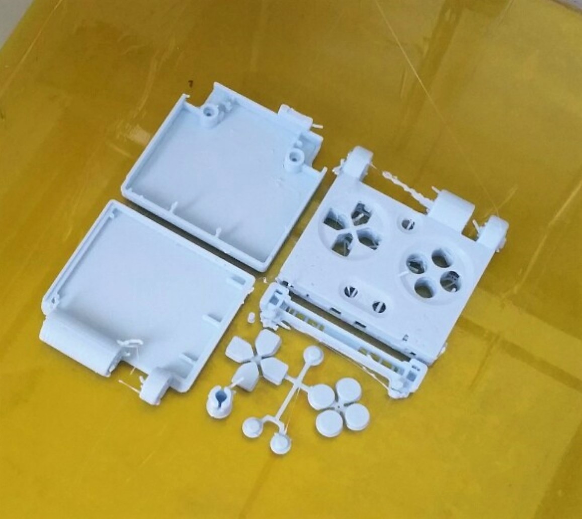
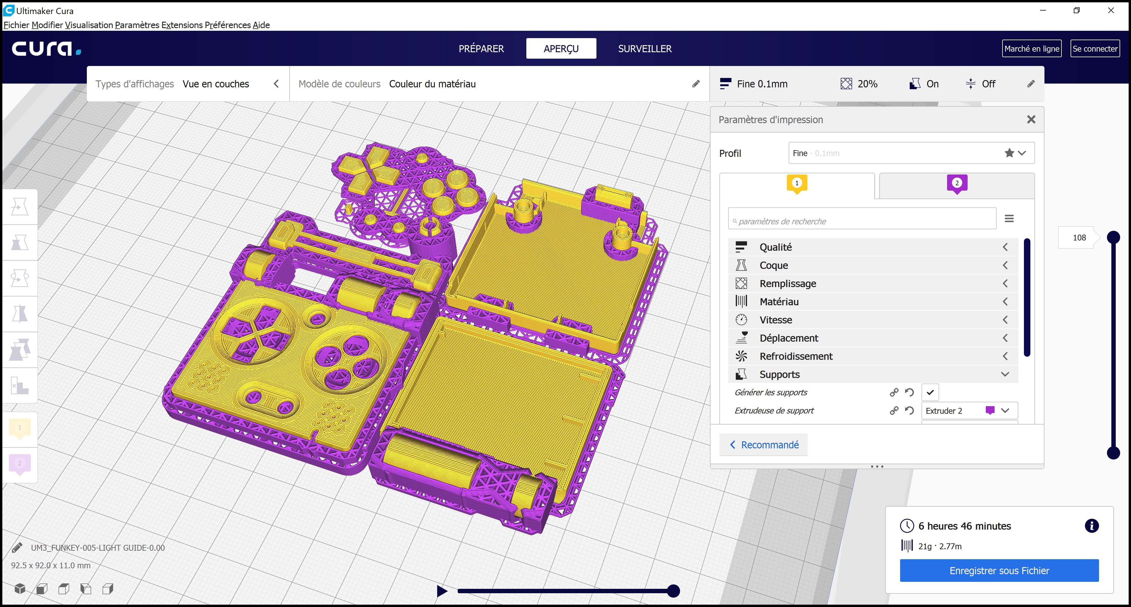
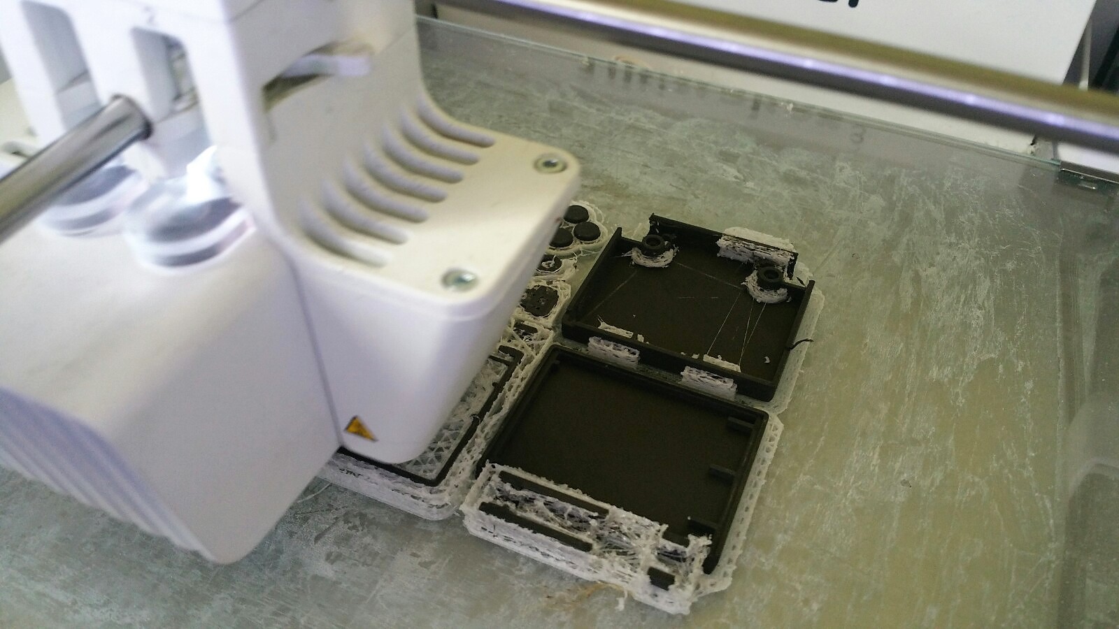
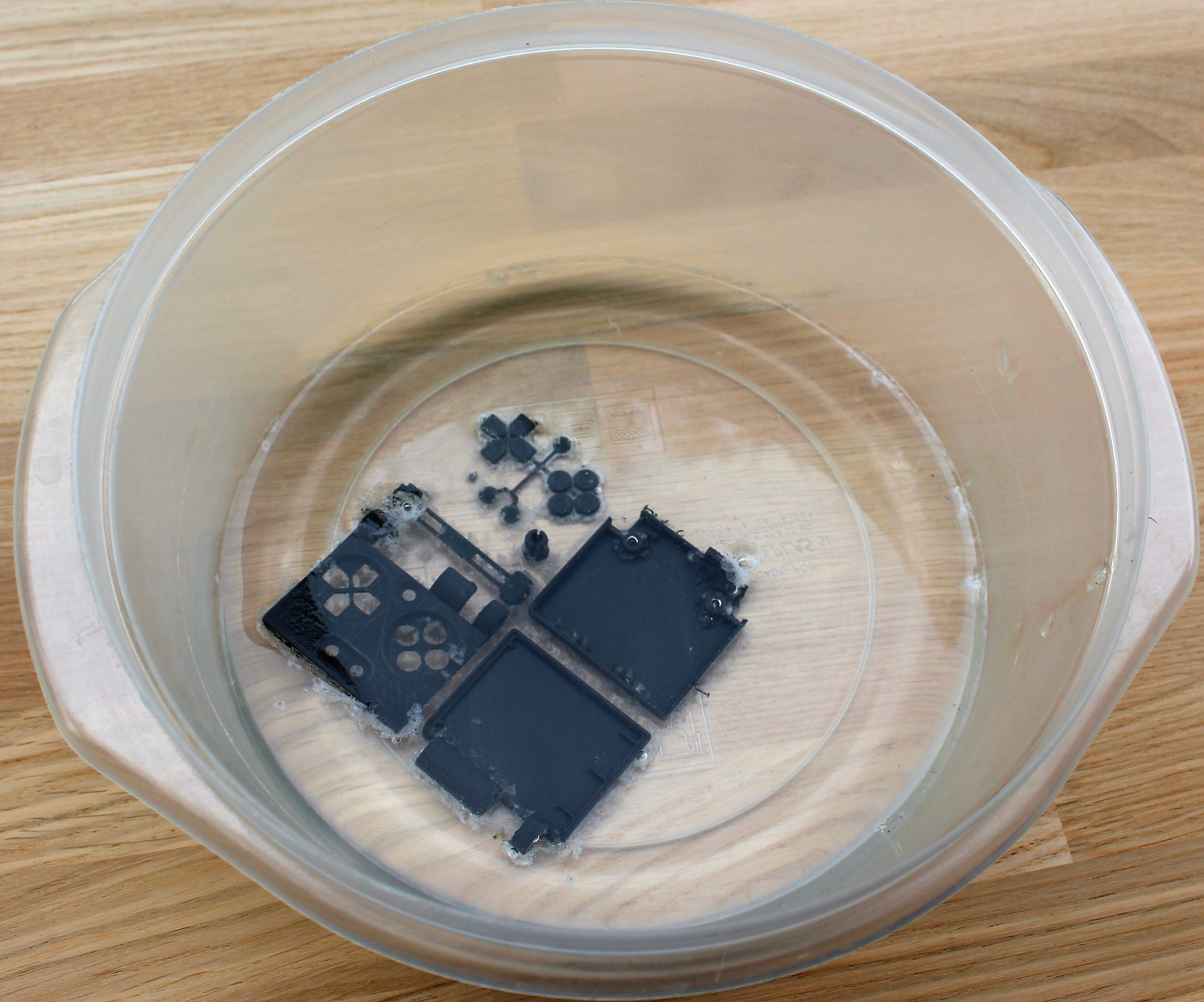
Below are the prints from an Ultimaker 3, nozzle 0.4mm, layer height 0.10 and double extrusion with standard PLA and water-soluble material.
![]()
![]()
![]()
![]()
![]()
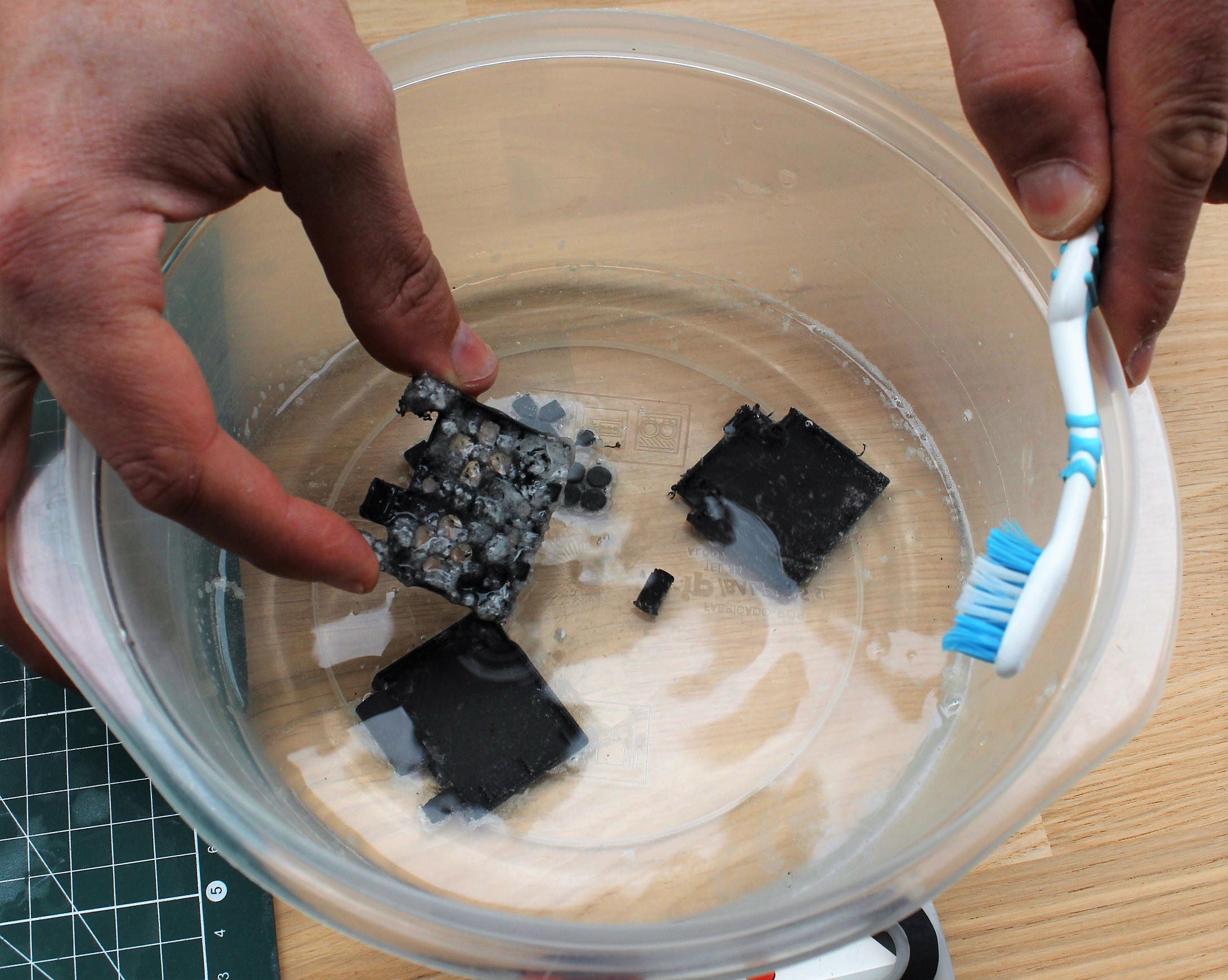
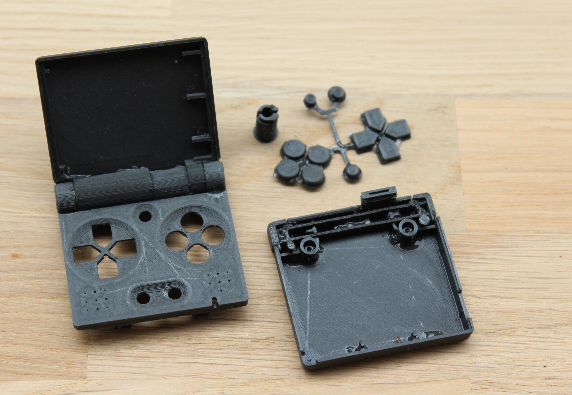
Here are the results after a one hour bath in cold water and some toothbrushing to remove the residues:
![]()
![]()
This technology (and the PLA used) is sturdy enough for our needs but, even if the printing params might not have been optimal, the surface finish and level of details are far from ideal. It is especially noticeable when we start putting together the different parts. The outer parts are ok but, even with soluble material, the inner parts needing supports material lack precision and surface finish.
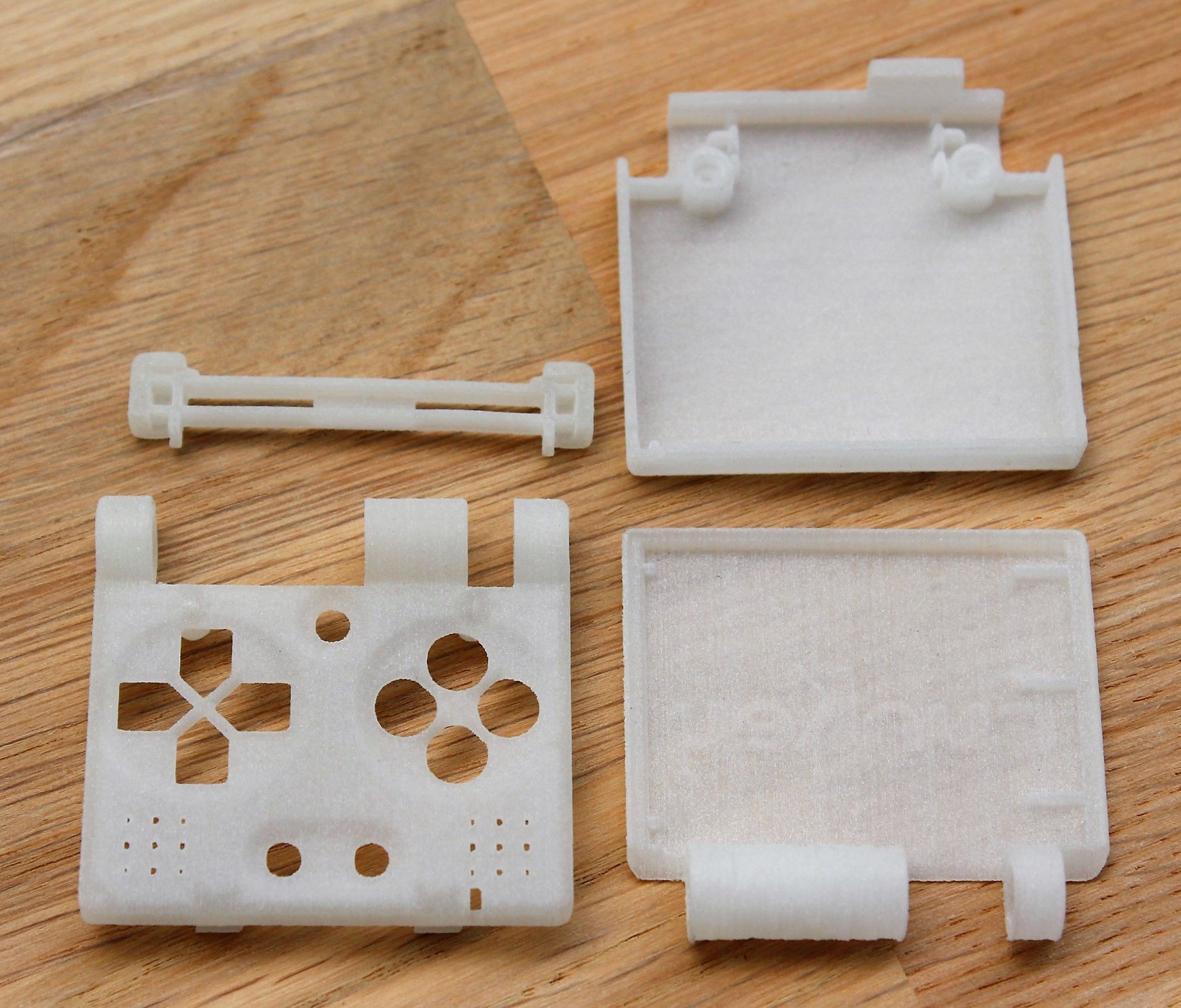
SLS
With this technology we have chosen to go with PP (Polypropylene) among the variety of available materials such as PA12, PA+GF (Glass Filled), PP (Polypropylene), Alumide (Mix between PA powder & aluminum powder), TPU92 (Thermoplastic Polyurethane)...
Here is how the prints turned out with Polypropylene:
![]()
![]()
This time the inner parts of the casing were the same quality as the outer parts. As you can see this material is too elastic though. But if materials can be swiched for sturdier ones, precision still falls behind our needs. Besides, surface finish is not smooth and the porous material quickly tends to absorb dirt.
SLA
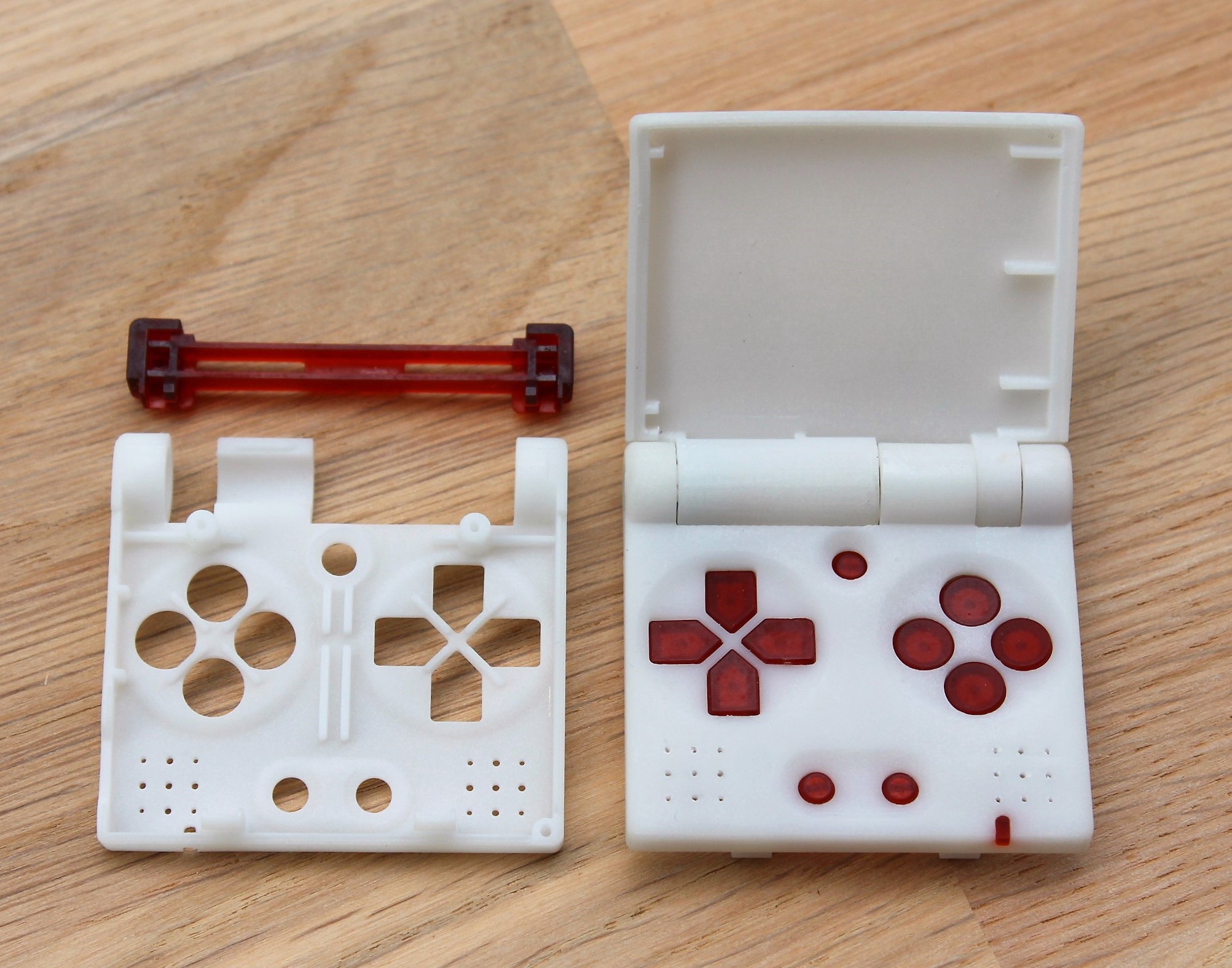
Different types of resin were tested with this technology:
- Somos® EvoLVe 128 ( white)
- Accura Xtreme (gray)
- R11 from Envisiontech (red transparent)
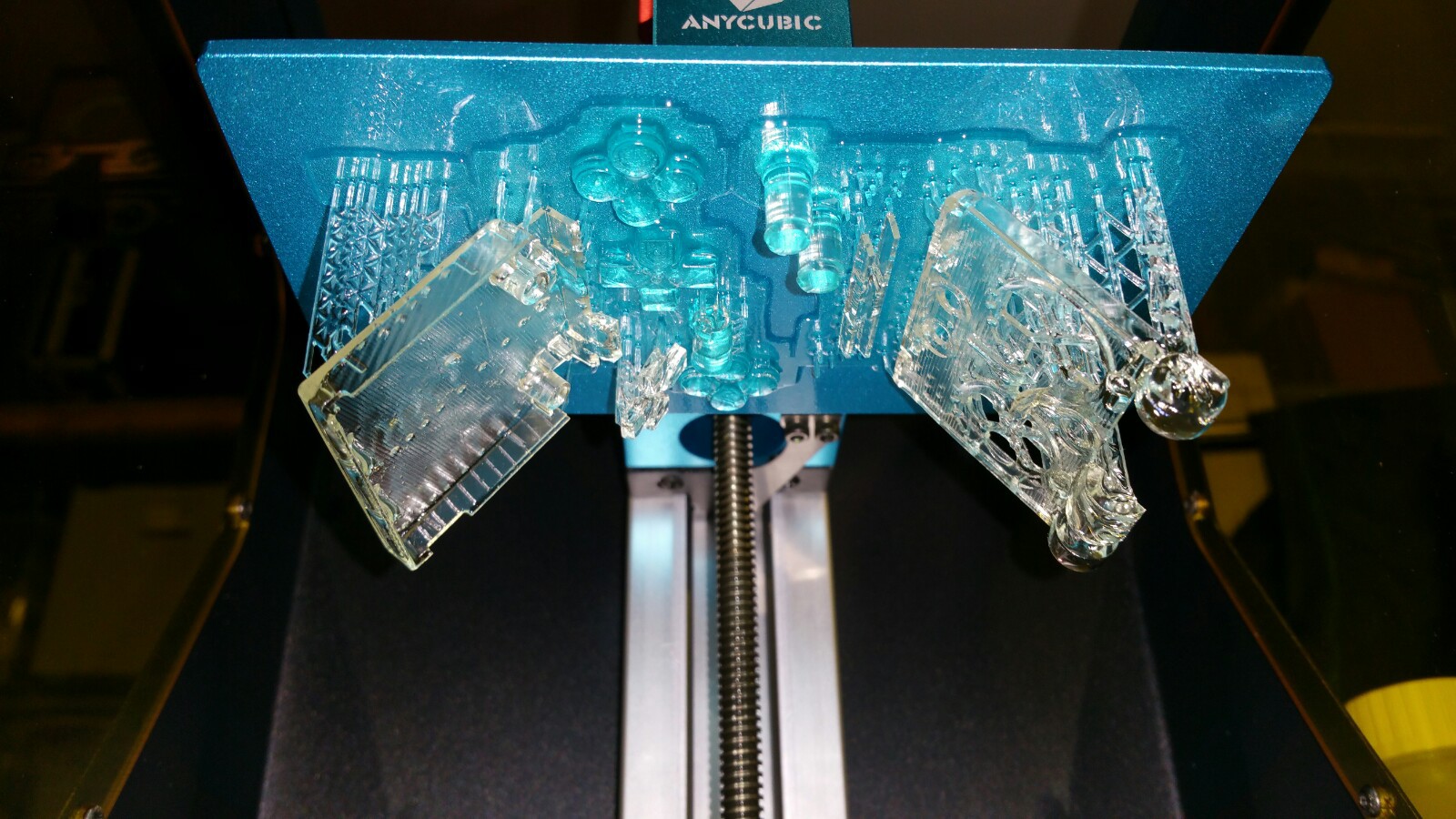
- ANYCUBIC resin (green transparent).
![]()
![]()
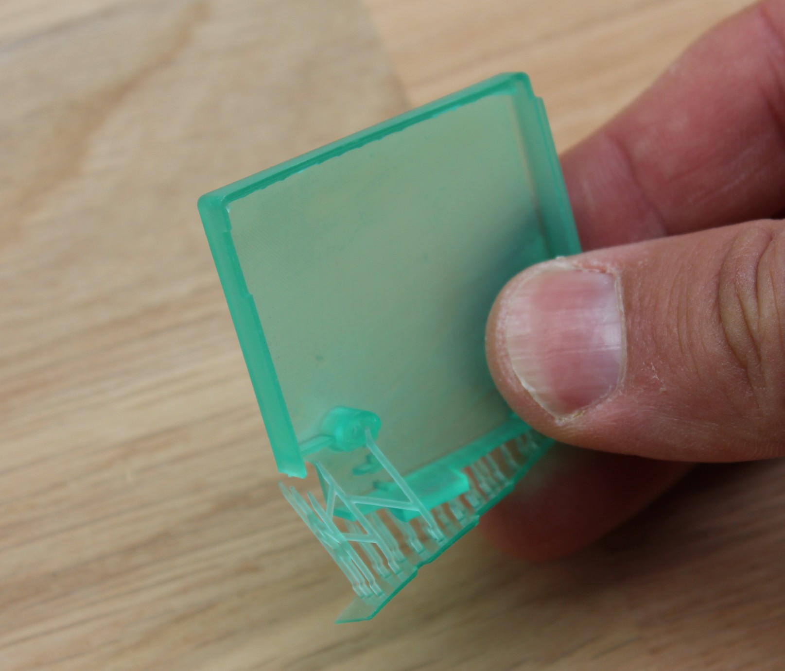
The biggest drawback with SLA printing would be that it is still very far from being as user friendly as FDM printers. Not only does the resin needs to be handled carefully in the first place but the post-processing treatments require one to not be afraid of a little chemistry. The prints must be cleaned with isopropanol alcohol, and after removal of the supports, they need to be strengthened with UVs. Also, the smell of all these products is not the greatest.
The results however are definitely worth it!
![]()
![]()
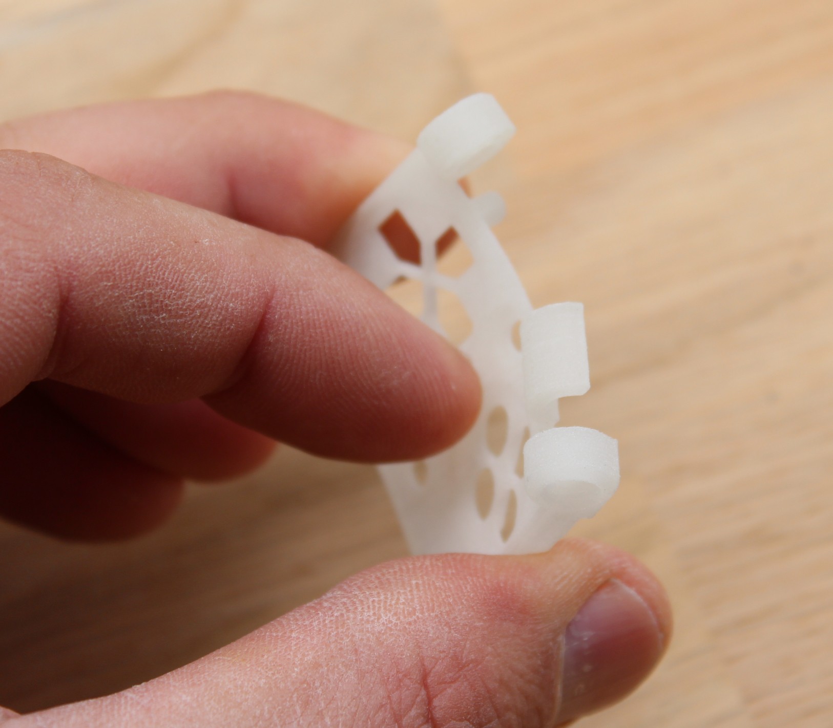
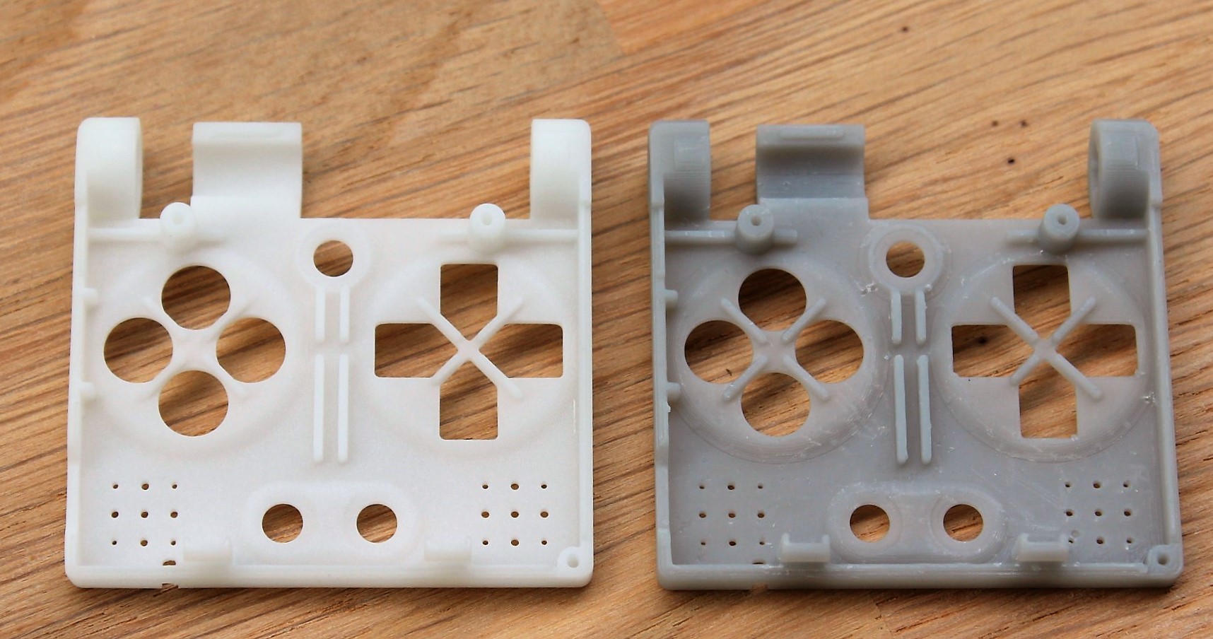
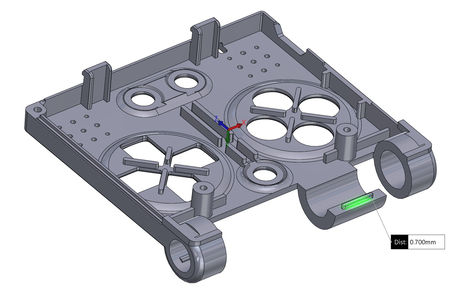
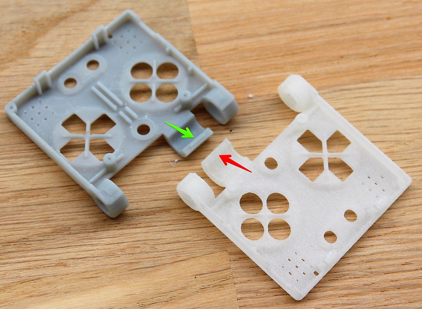
A great exemple of the kind of precision that can be achieved without a sweat by SLA technology would be the tiny plastic rib depicted in the image below.
It needs to be precisely 0.7mm wide and printed over a part that would need support with FDM technology.
![]()
As can be seen in the picture below, only SLA achieves this level of precision (gray casing) with a very neat rib while even SLS (white casing) clearly falls behind.
![]()
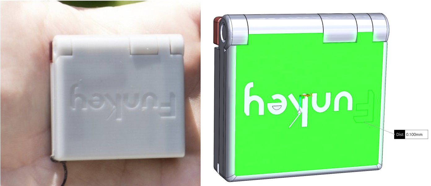
Here is another example of the kind of precision achieved with SLA: the FunKey logo is only extruded 0.1mm in the casing. As you can see it is not only clearly visible but also very neet on the SLA print. This is not the case with other technologies that printed the same STL file.
![]()
We noticed our SLA prints were quite fragile however, this material is a bit more breakable and one needs to be careful when assembling the parts, espacially with the screws. They need to be put gently not to break the shanks.
Precision: theory vs reality
Theoritically here is the precision that each technology can achive in average:
- FDM: ± 0,15 % (lower limit with standard nozzle at ± 0,2 mm), layer height: 0.05 to 0.3mm
- SLS: ± 0,3 % (lower limit ± 0,3 mm) / layer height: 0.12mm
- SLA: ± 0,2 % (lower limit ± 0,2 mm) / layer height: 0,05 to 0,2 mm
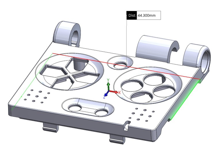
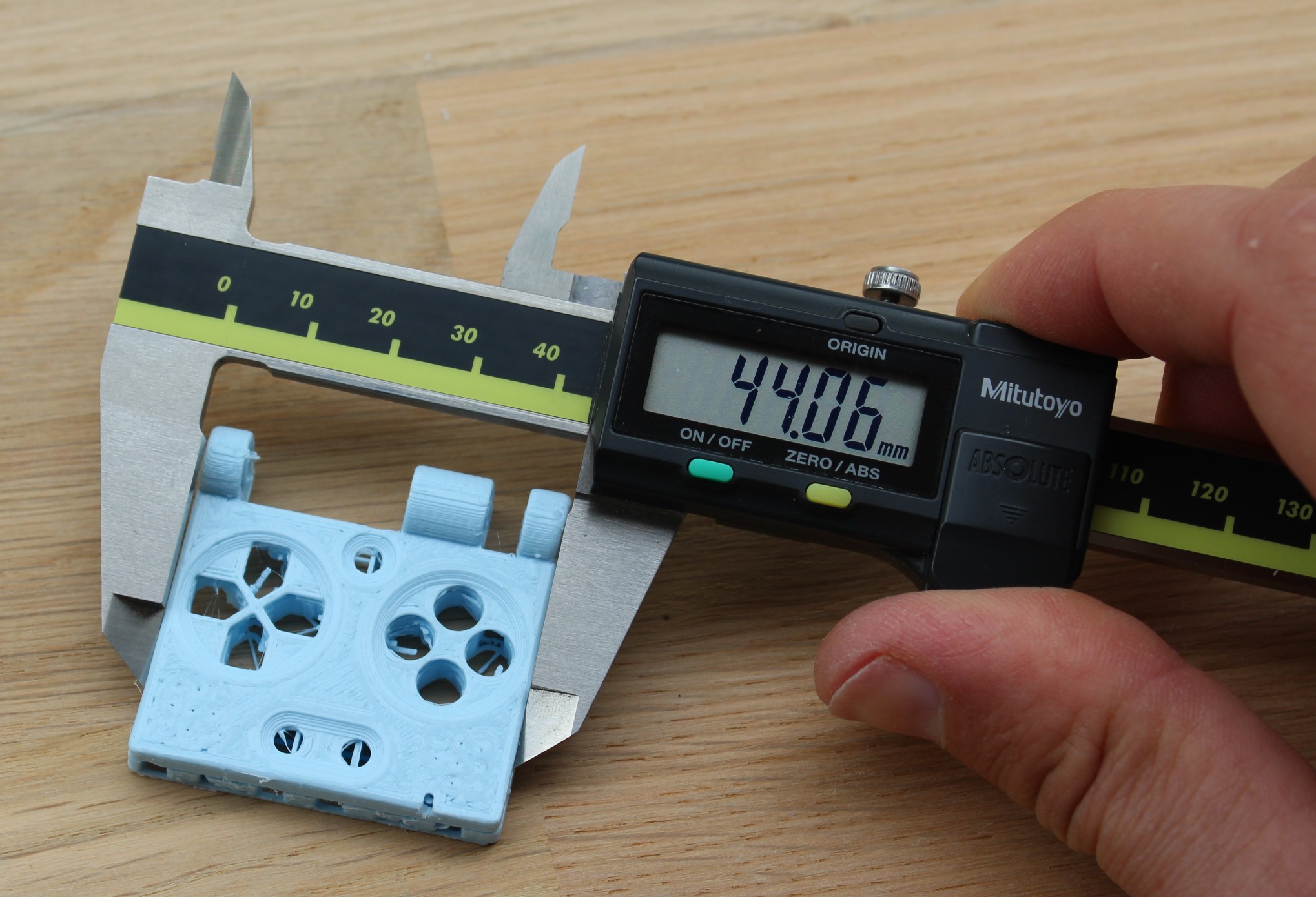
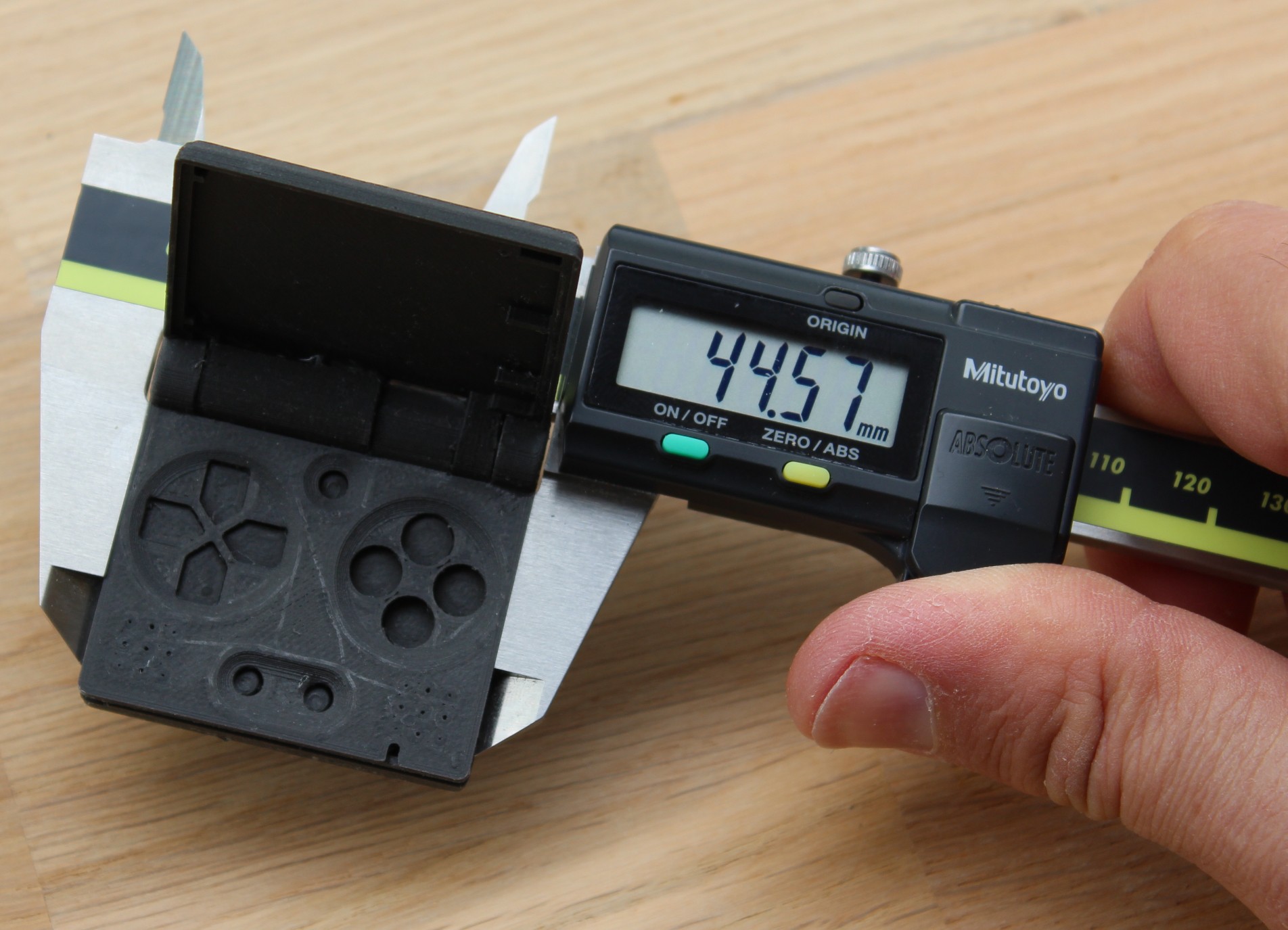
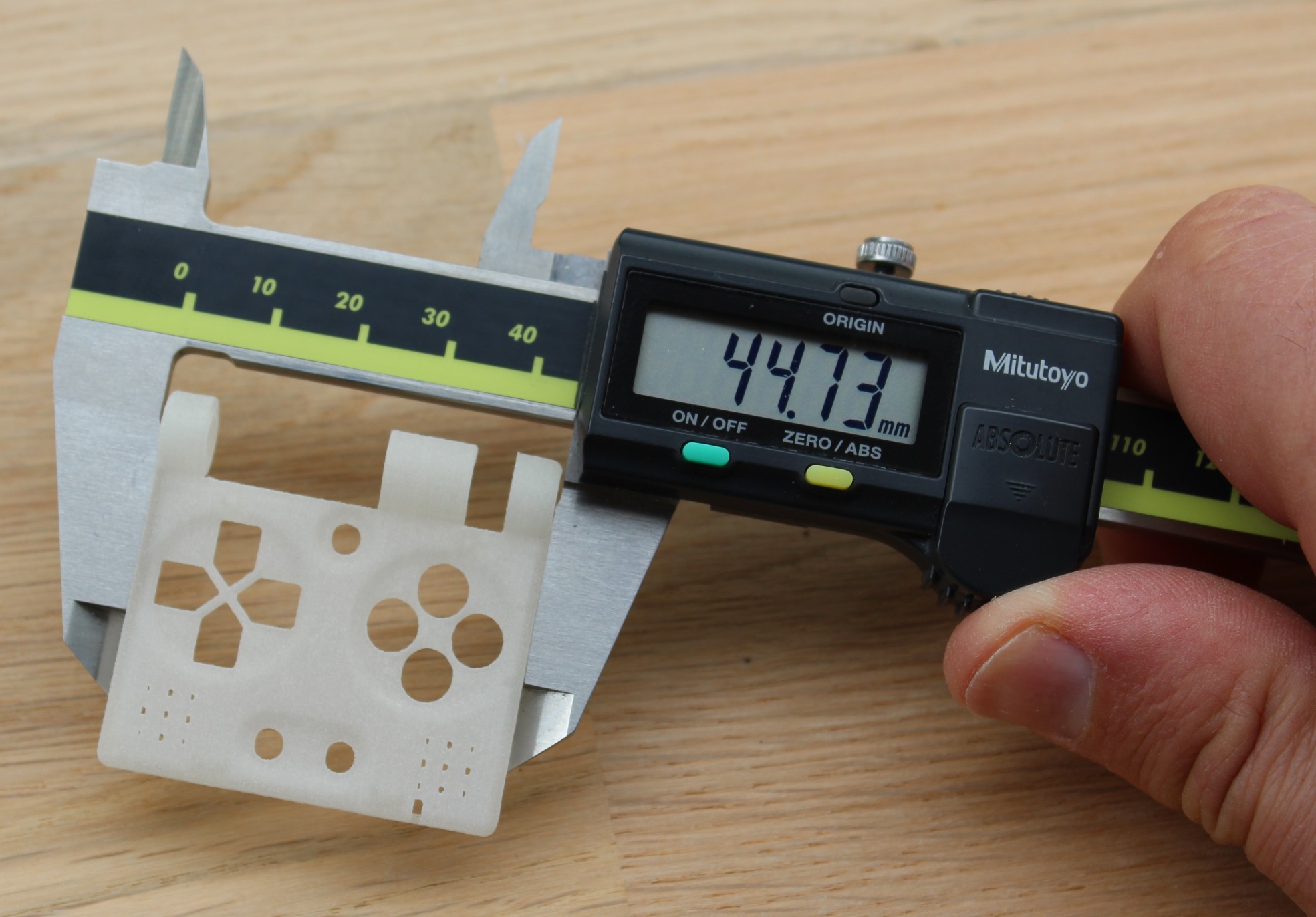
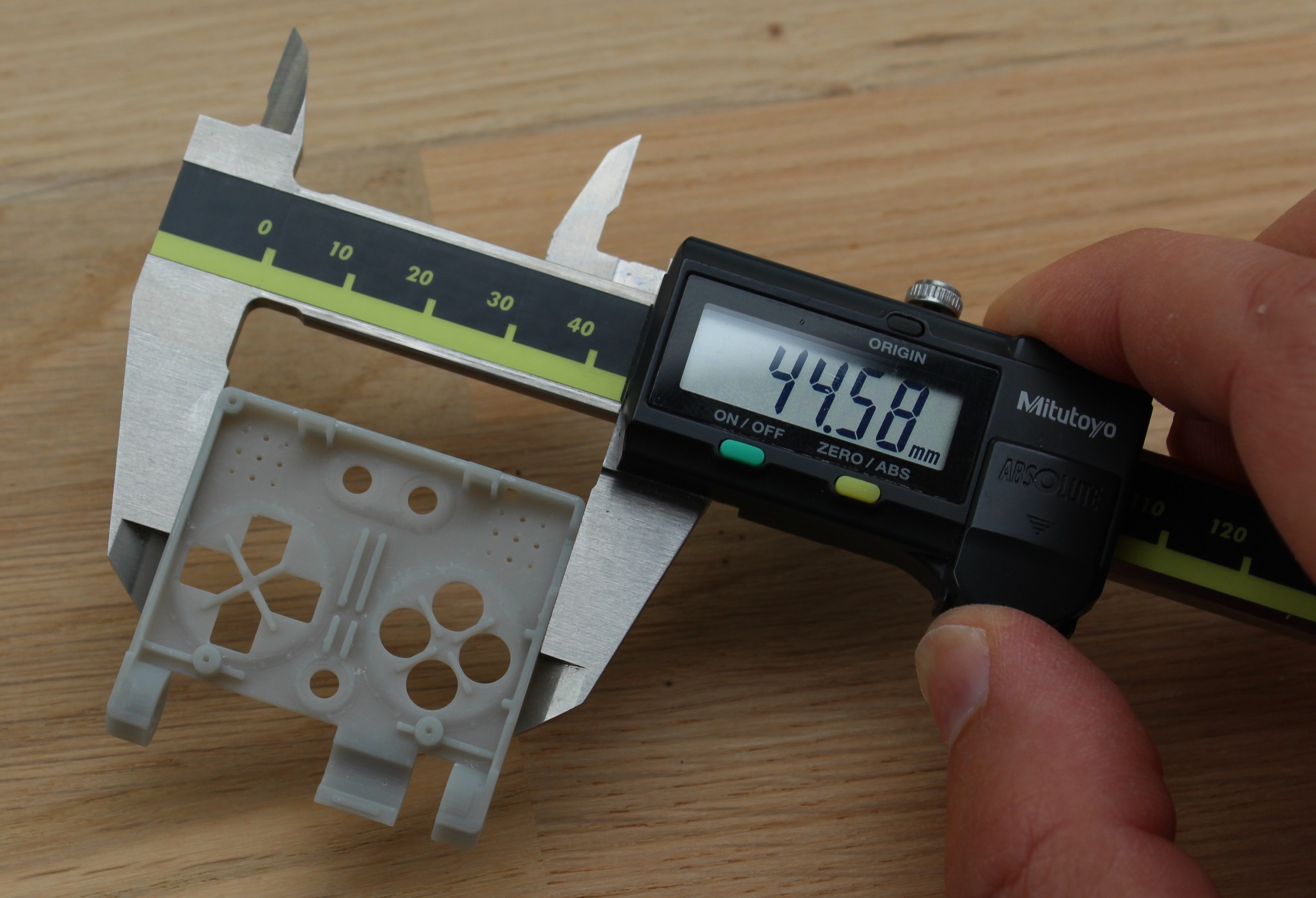
Below can be seen different measurements of the casing's width (theoritically 44,3mm)
![]()
FDM :
![]()
![]()
SLS :
![]()
SLA :
![]()
Globally all three technologies are decent, it is the level of details that lacks for SLS and especially FDM compared to SLA.
![]()
Conclusion
This log does not pretend to be an extended research on 3D printing technologies but merely an attempt at finding the one best suited for trying out our prototype before production. Keeping this in mind we might not have set the very best parameters for FDM prints and they might be greatly improved, but our conclusion would be that in order to achieve the level of details FunKey needs, SLA technology is simply one step further regarding accuracy and surface finish.
We encourage anyone however to print Funkey with their own setups and tell us about the results. All the files are available here or on thingiverse and grabcad.
Thanks to the SLA prints we were able to validate our design choices regarding the integration of the electronic components, the new screen with its flex and the strength required to open/close the hinge. It also allowed us to see where our design could be improved, for example by decreasing the led brightness, reducing the logo's size, adding some matter to block the light from the display backlight, ... and some other things that we will detail in a dedicated log.
We are now working on fixing these small issues and printing new SLA versions to validate them and then be ready for injection molding (probably in ABS). We intend to show in a future log the design rules that were applied to conceive FunKey's plastic parts for injection molding (Draft angle, injector pin, injection gate, cavity, core…).
-
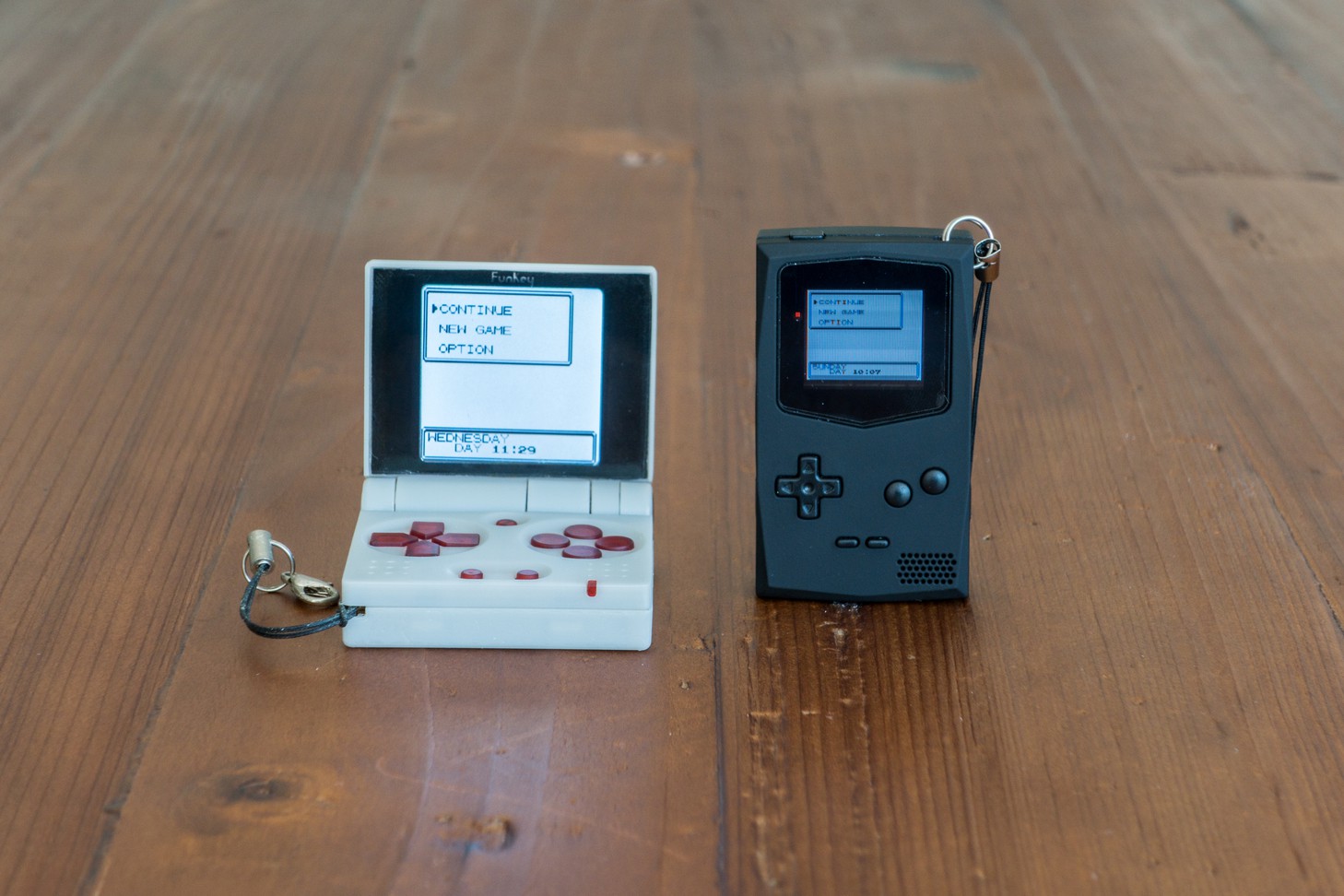
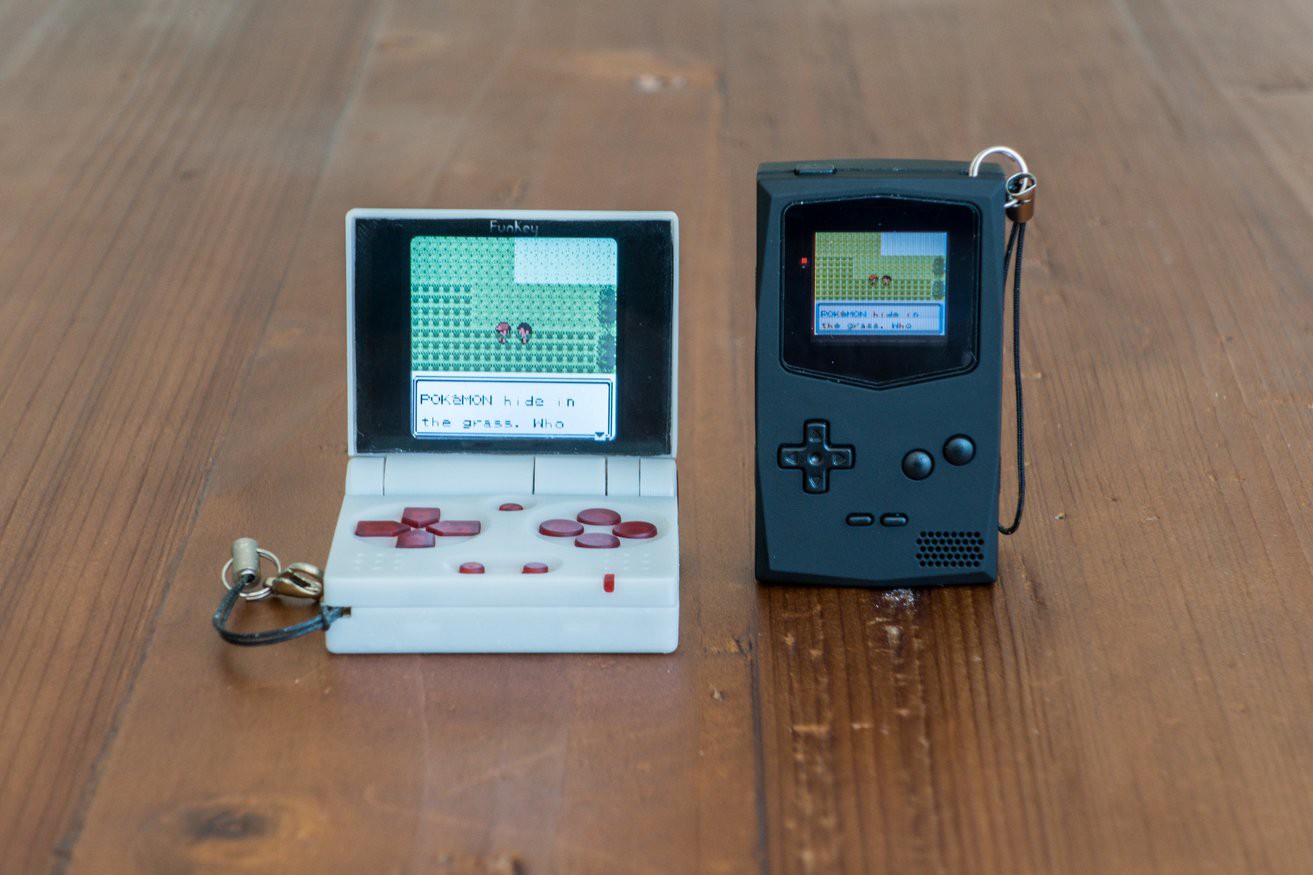
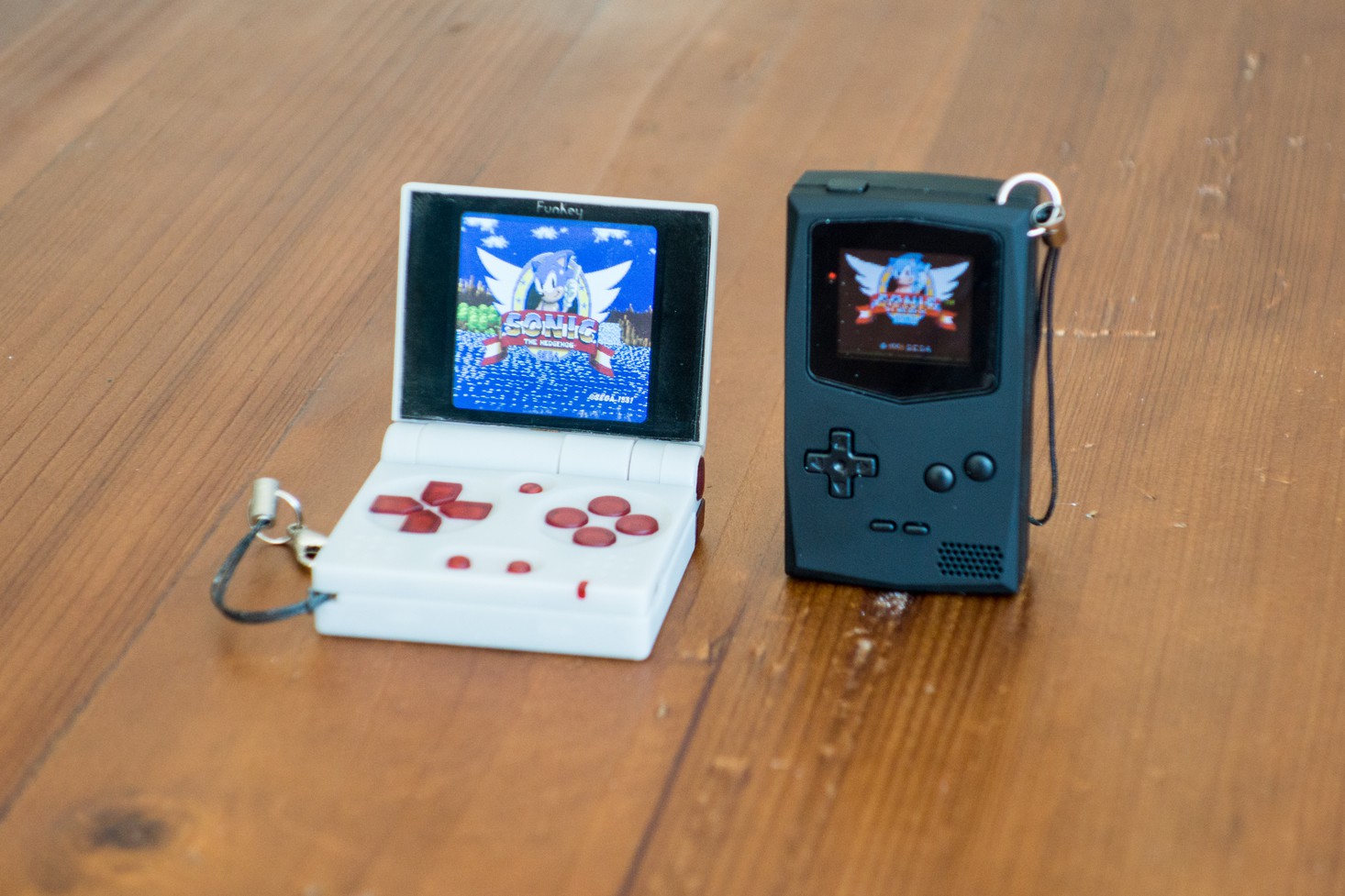
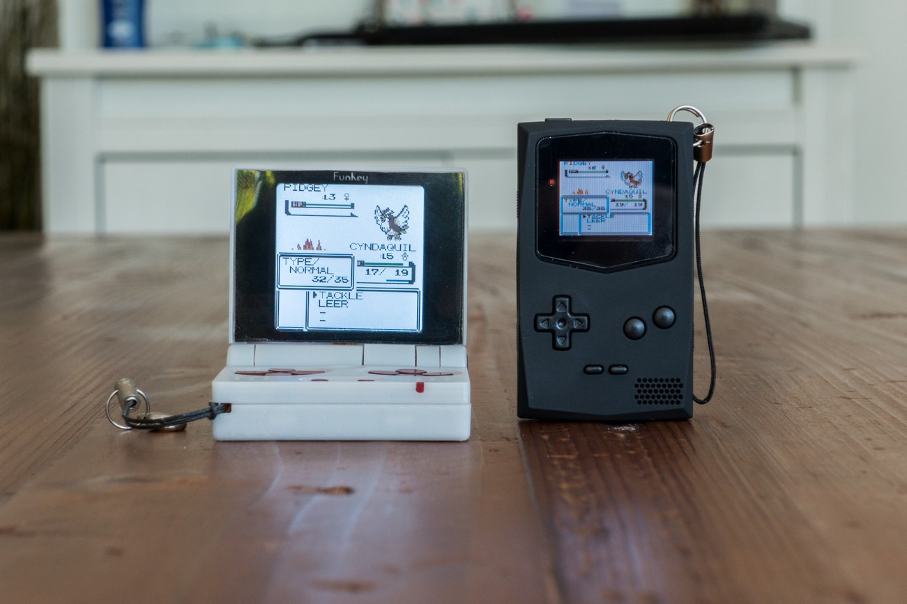
Photo shoot side by side with PocketSprite
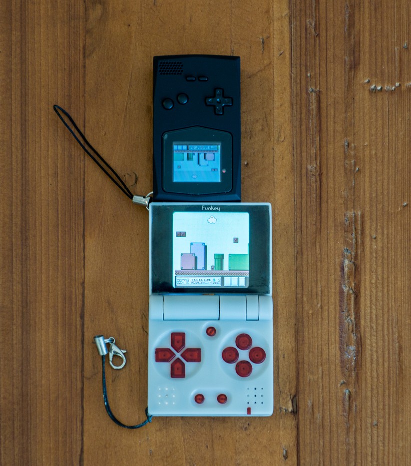
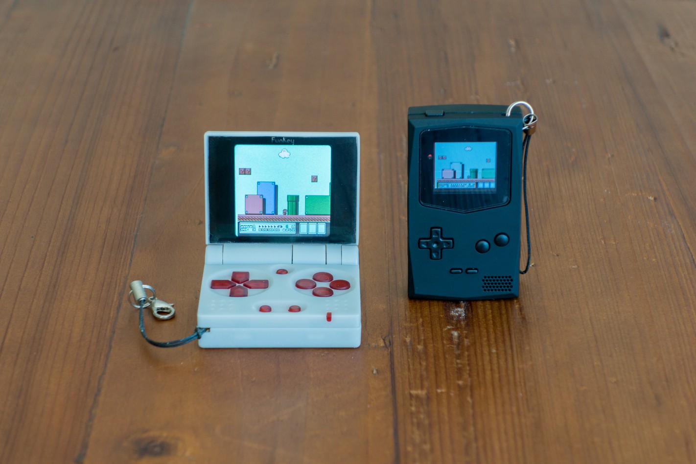
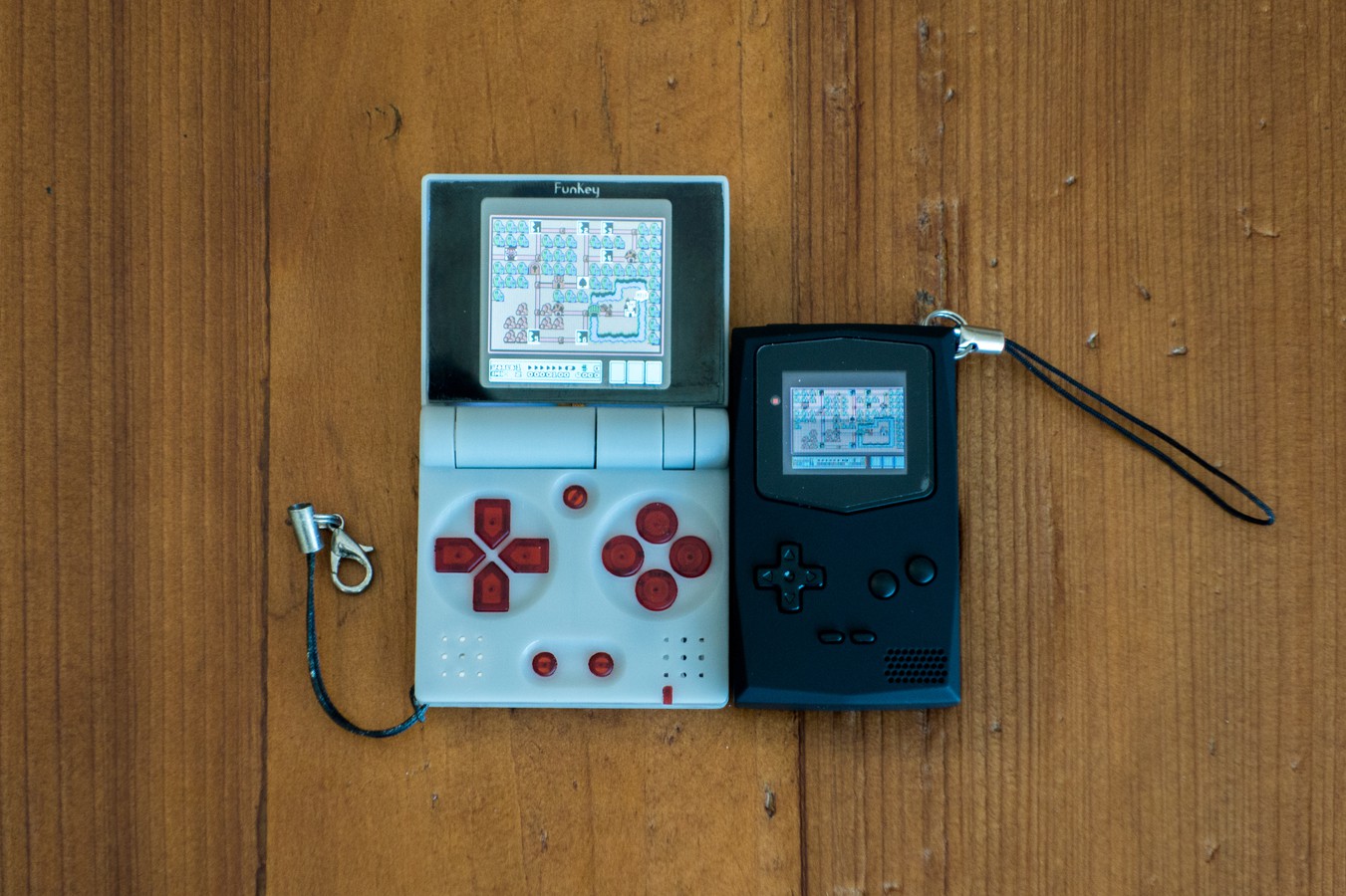
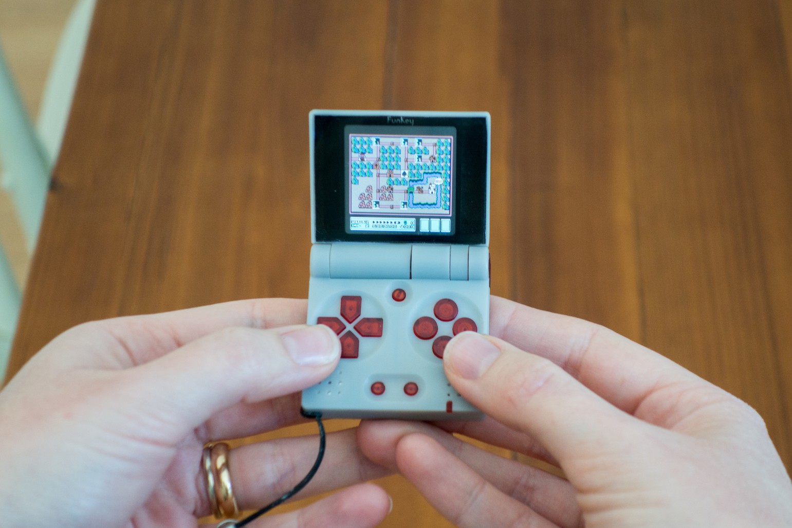
05/01/2019 at 10:27 • 0 commentsIf you are on this page you might already know about the PocketSprite. For those who don't it is the tiniest keychain-sized console, born from a crazy tiny gameboy project introduced in 2016 by SpriteTM. It was this project that inspired our first Keymu gaming console. We encourage you to go on Keymu's page if you want to know more about how FunKey started.
A few years later SpriteTM eventually launched a successful crowdfunding campaign and from there went to production to build and sell the PocketSprite. As for the PocketSprite's initial prototype that inspired our first Keymu prototype, it is now PocketSprite's production success that inspires us to do the same with FunKey.
Keymu's idea - then forwarded to FunKey - was to build our own version of SpriteTM's first prototype from scratch while improving where we thought it could be done. As for mechanical design this translates mainly in FunKey's clamshell design which allows to fit a wider screen, larger buttons to play comfortably, a bigger battery and all this while keeping a very tiny form factor.
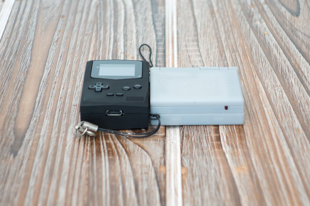
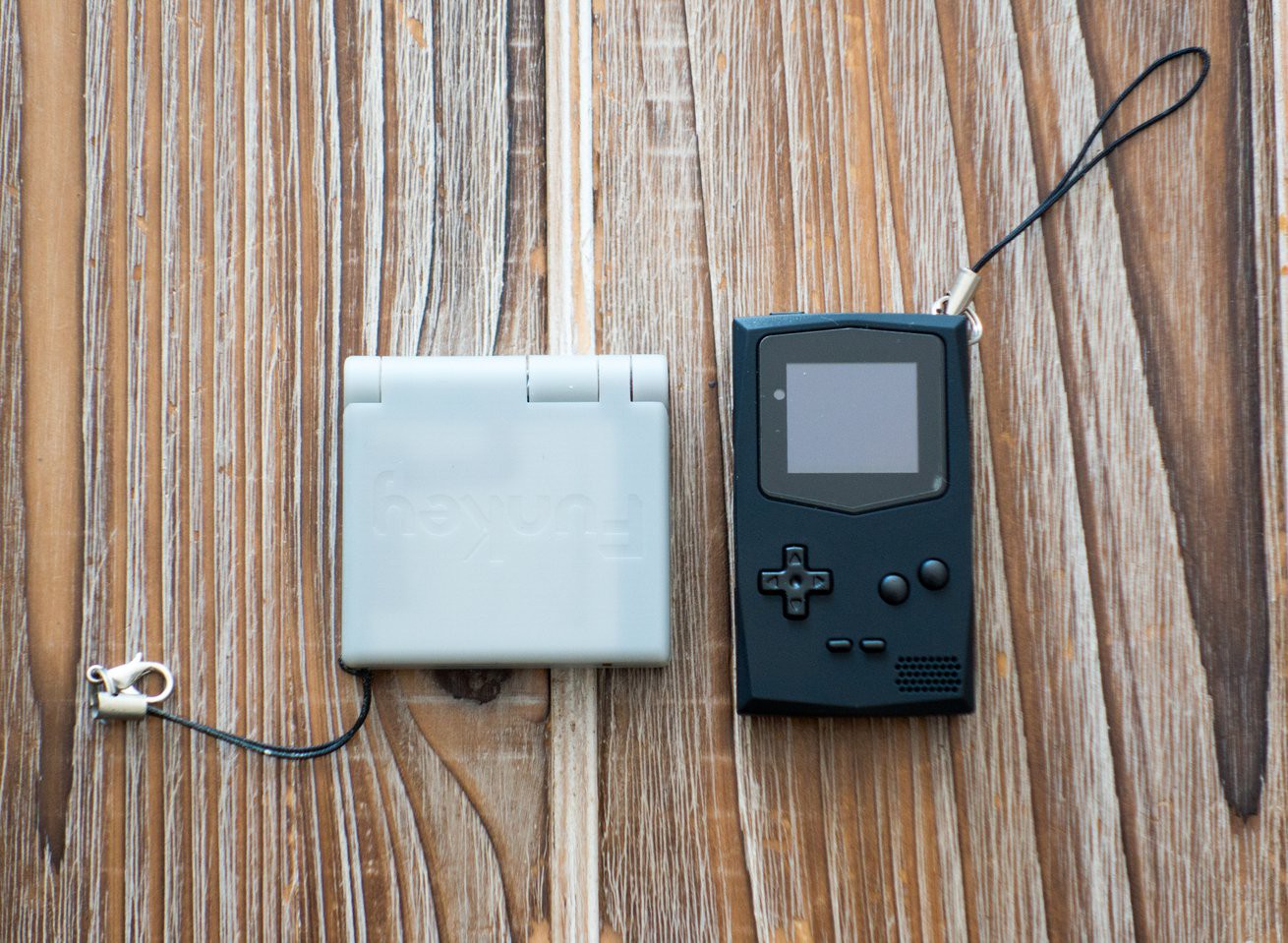
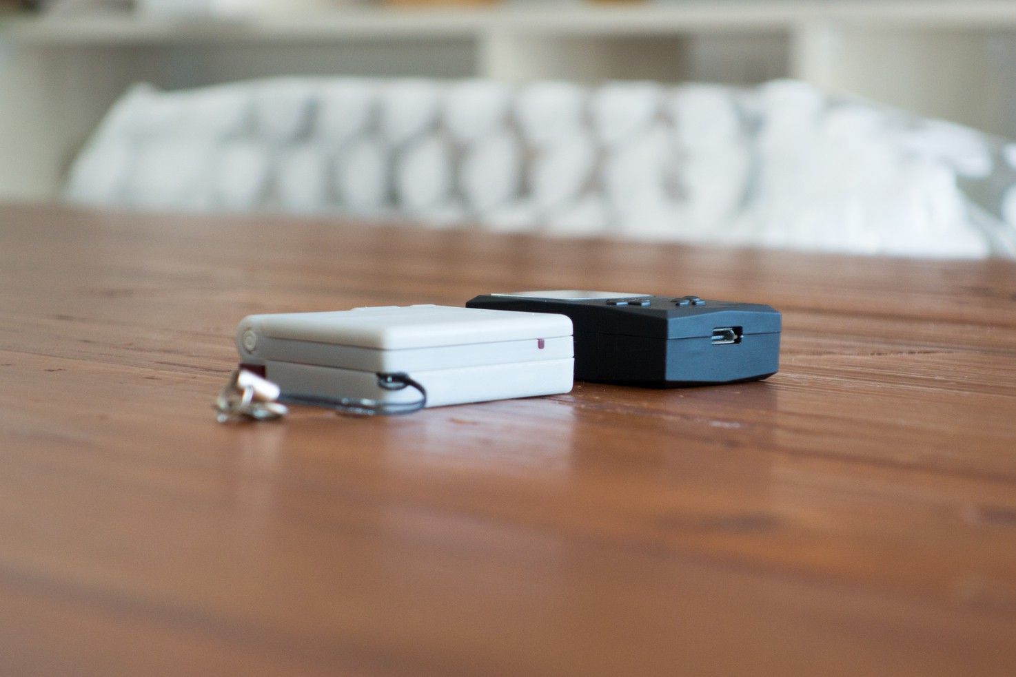
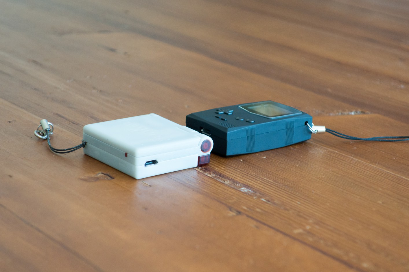
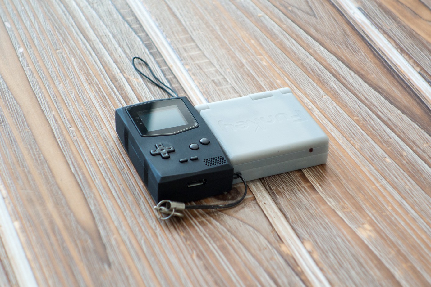
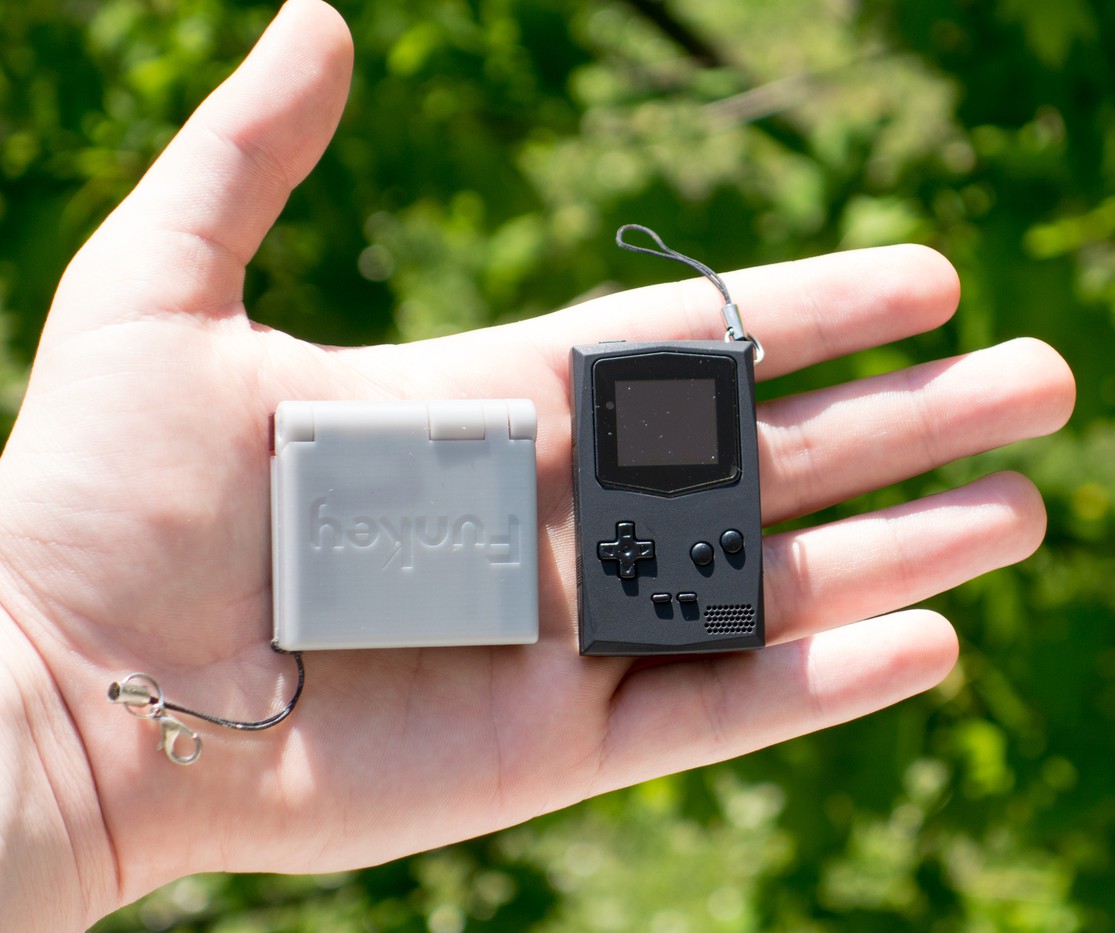
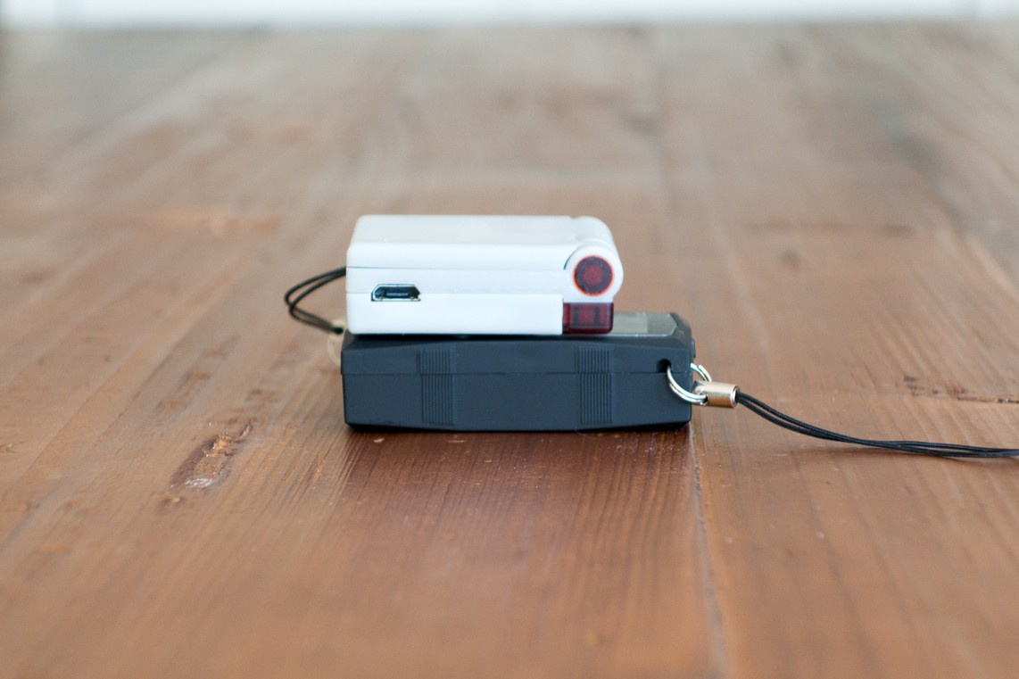
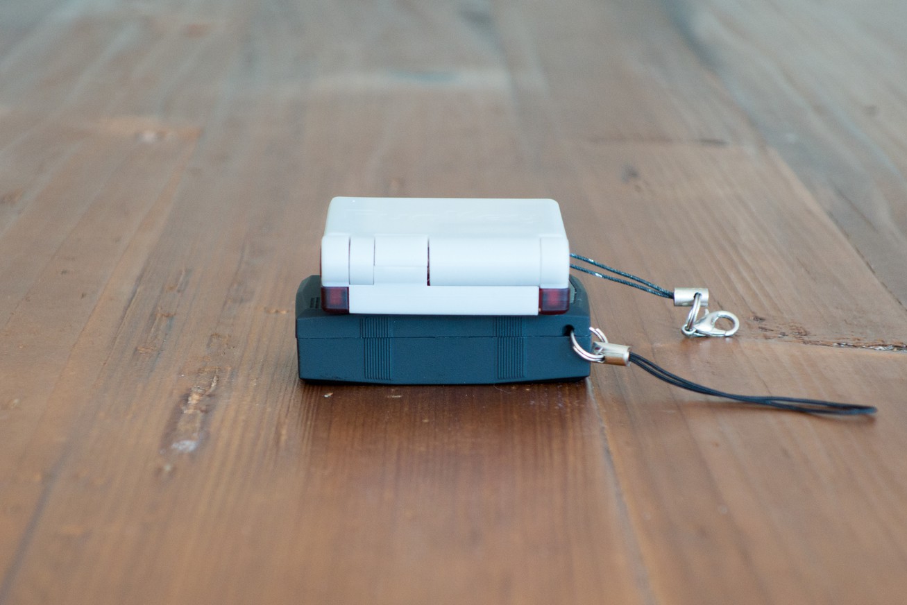
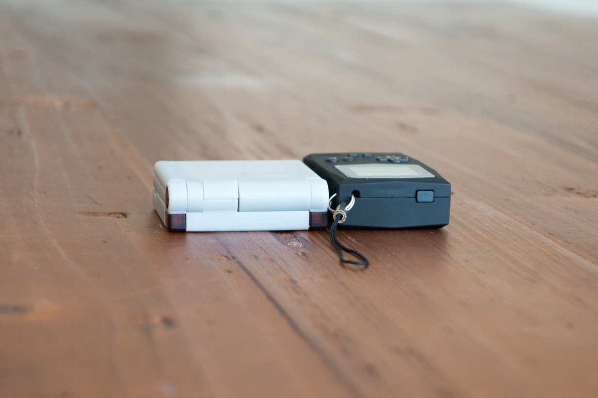
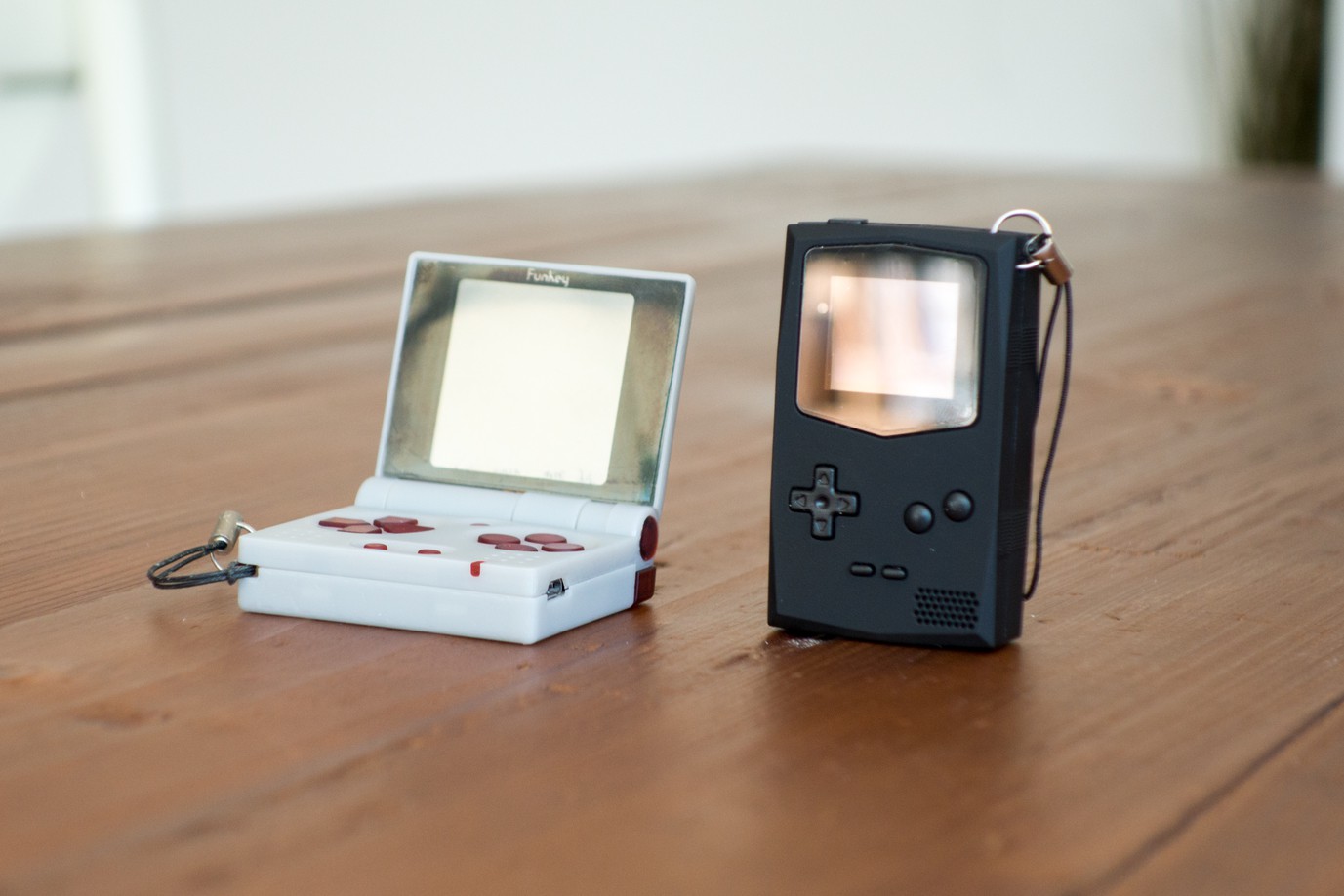
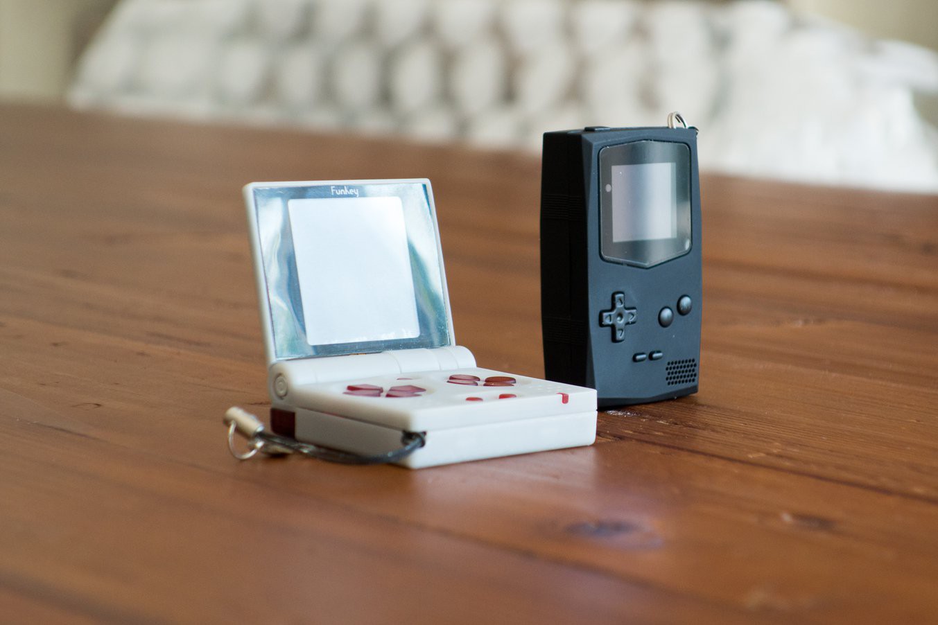
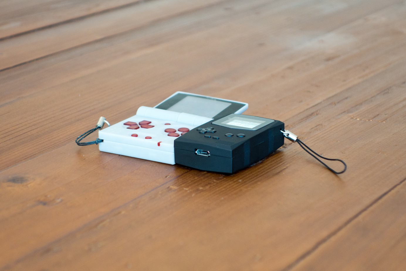
But photos are worth a thousand words so here they are:
![]()
![]()
![]()
![]()
![]()
![]()
![]()
![]()
![]()
![]()
![]()
![]()
![]()
![]()
![]()
![]()
![]()
![]()
![]()
![]()
![]()
![]()
![]()
![]()
-
Schematics: SPI LCD
04/30/2019 at 22:06 • 0 commentsSPI LCD Screen
One of FunKey's strong point is certainly its screen: in a chosen form factor of roughly 45x45x15mm (1.75x1.75x0.6"), it has to be comfortable enough to provide a good gaming experience.
If in theory this allows to shoehorn a 2.4" (diagonal) square screen, in practice, these screens are seldom square and more rectangular in shape.
Unless you are a large manufacturer and selling millions of devices, you are limited to using the screens that are available on the market, which most of the time were designed for a long-forgotten specific devices (think of PDAs, MP3 players, clam-shell phones, pods, etc.) and standard aspect ratio are either 5:3 or 16:10. Thus, for a given pixel technology, this results in rather standard screen sizes.
So the next size down is 1.8", but these screens tend to be quite thick and based on an old technology, so their typical resolution is rather limited @ 128x160 pixels: too small for gamers.
Still going down in size, you can find 1.5~1.55" screens with an interesting resolution of 240x240 or even 320 x 320 ("Retina") pixels, but most of them use a fast and complex MIPI DSi interface requiring a dedicated controller on the host side. These screens were popular as the screen used in 6th-generation iPods, but unfortunately, getting a retail CPU with a MIPI DSi interface is almost impossible.
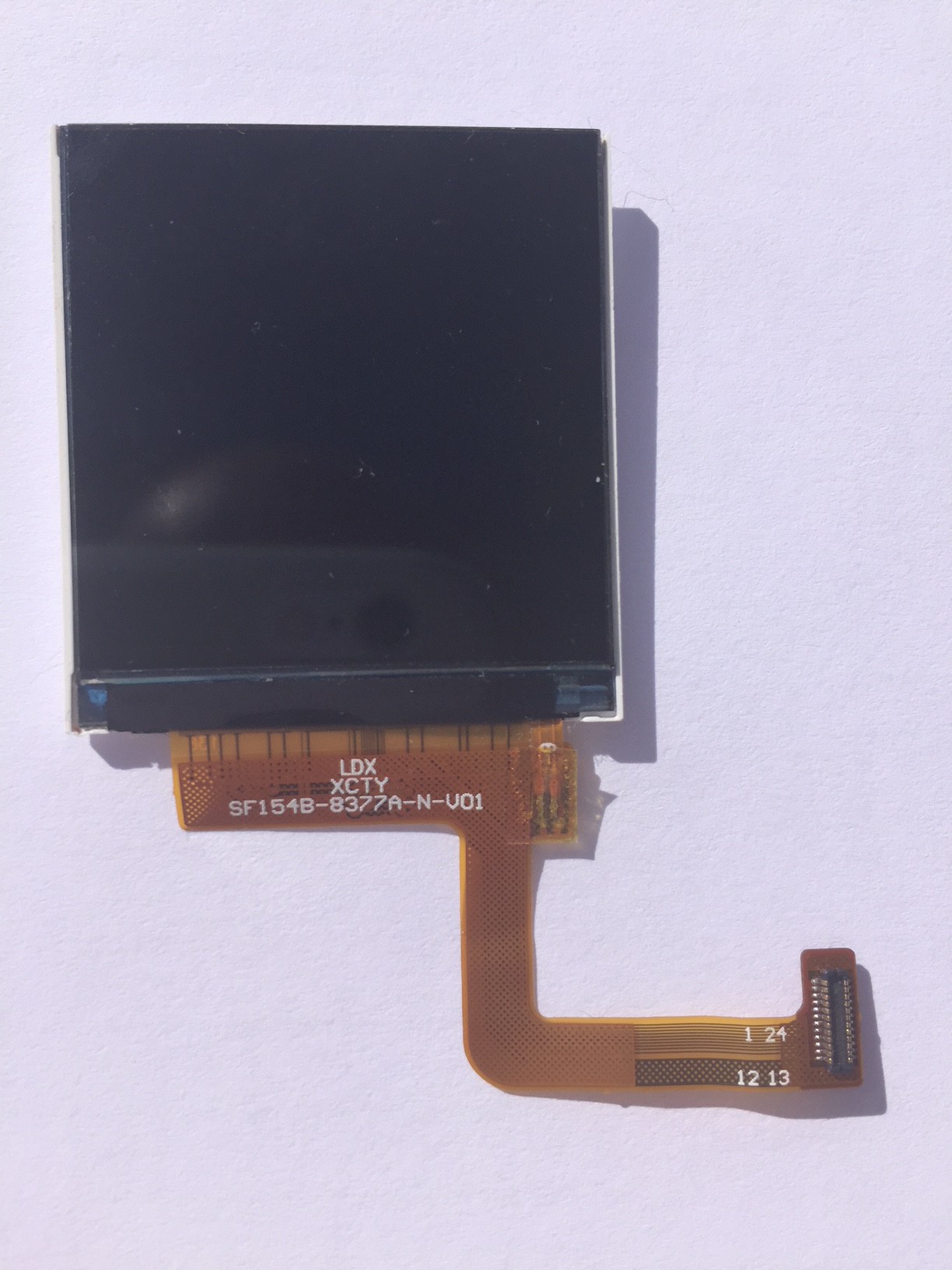
Fortunately, we found this 1.54" LCD screen on AliBaba:
What makes this screen remarkable is its standard SPI interface, which like the MIPI DSi one, only requires a few wires and thus a narrow flex cable, easy to roll into a hinge.
This 1.54" display has 240x240 16/18-bit full color pixels and is an IPS display, so the color looks great up to 80 degrees off-axis in any direction.
Be careful though, as in order to achieve a 30 fps @ 240 x 240 pixel resolution in RGB666 (3 bytes / pixel), this requires a ~40 MHz SPI clock rate. Once again, we were fortunate as both the V3s CPU and the screen built-in controller (a Sitronix ST7789V) support this high clock speed (after checking with the manufacturer and despite the controller datasheet specifies only a serial clock cycle (Write) of 66 ns or 15 MHz!).
We were even luckier as its backlight consists in 3 white LEDs in parallel and not in series, such that no additional step-up DC-DC converter is required, as a standard 3.3V / 60 mA (typical) power supply is sufficient. Of course, we won't be able to drive this current directly from a CPU GPIO and the backlight will require an additional transistor to interface to the LCD backlight.
Its flex cable requires a mating Hirose 0.4 mm pitch DF37NB-24DS-0.4V dual row SMT connector, out of which only one single row is actually used.
Schematic
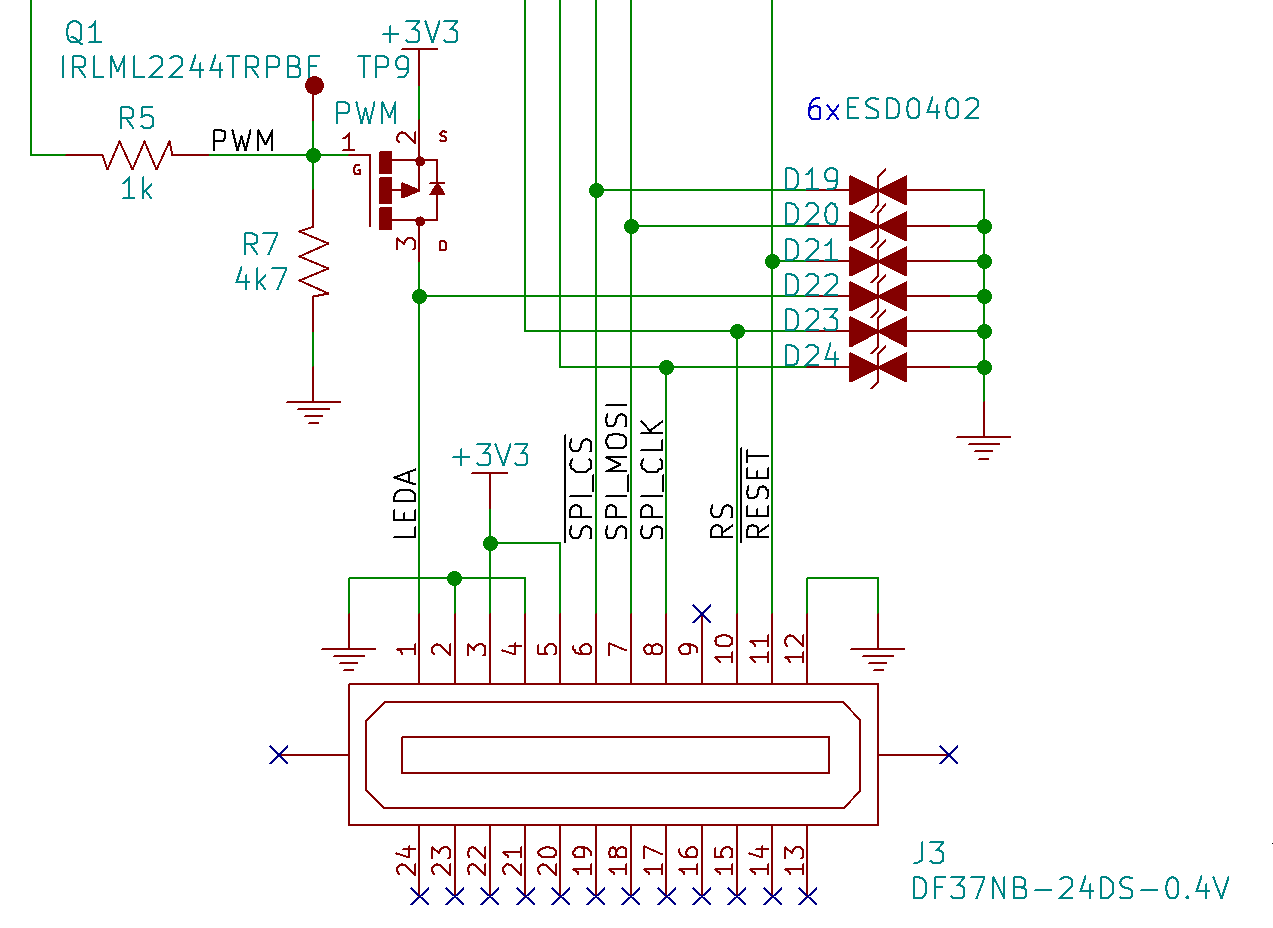
The schematic is thus quite simple:
![]()
The main component is of course the Hirose screen connector J3, with the following signals:
- LEDA: the backlight LED Anode connection (+)
- GND
- +3V3 power supply
- /SPI_CS: SPI Chip Select
- SPI_MOSI: SPI Master Out / Slave In
- SPI_CLK: SPI Clock
- RS: LCD-specific Register/Memory Select (or Data/Control Select)
- /RESET: LCD Reset
All data signals feature an ESD TVS protection diode D19-D20, and except for the power supplies and LEDA + /RESET signals, all signals are directly connected to the V3s CPU's SPI interface, so there is not much to say about these.
The /RESET signal is currently tied to the PMIC PWR_OK output, but in a future revision, we plan to change this so it is instead controlled from a CPU GPIO pin.
Backlight PWM
The backlight control requires a few more components: a MOSFET-P transistor Q1 and 2 resistors R5 and R7 to provide its polarization, more on this below.
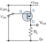
As the backlight LEDs cathode (-) pin are directly tied to GND within the screen, we need to drive these LEDs "from the high-side", i.e. between the +3V3 power supply and the LEDA pin, so a MOSFET-P transistor is necessary:
![]()
As we want the backlight to be on by default, we need to drive it to GND by default: this is the role of R7. The role of R5 is then to make sure that -Vgs is driven below its threshold voltage and turns off the transistor when the CPU drives a GPIO high.
As an ultimate sophistication, we can drive the backlight from the CPU using one of its PWM built-in controllers with a varying duty-cycle, thus controlling the LCD backlight brightness accurately.
-
Schematics: DRAM Power
04/26/2019 at 21:10 • 0 commentsThe attentive reader may have noticed that the PMIC covered in the previous log only provides 2 out of the 3 required DC-DC...
This is because the AXP20x is originally the PMU (Power Management Unit) used by most Allwinner SoCs (A10, A13 and A20), which do not integrate SDRAM, so the board designer has a wide choice of memory option: DDR2, DDR3, DDR3L, LPDDR3, LPDDR4 with various voltage requirements.
But no specific PMIC was created for the Allwinner V3s used in the FunKey device which however integrates a fixed SIP (System In Package) 512Mbit (64MB) DDR2 SDRAM.
We thus have to design a separate SMPS (DC-DC) power supply for providing the +1.8V 1A required for the DDR2 DRAM power supply.
For this purpose, we followed closely the Allwinner Reference Design which provides the same circuit, based on common pin-compatible SY8088 or LP3220 Chinese Buck DC-DC converter chips. But since these chips are not easy to provision in our place, we replaced it by a performance and pin-compatible AP3418KTR-G1 chip.
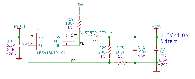
Here is the corresponding DRAM Power schematics:
![]()
Nothing very fancy here: the SMPS chip U4 has its required input filter capacitor C37 and output capacitors C65 and C73.
The low-profile ferrite-core power inductor L6 (rated with a saturation current of 1.76A and low < 0.1 ohm resistance) provides the DC-DC energy storage element.
The R20 / R23 precision voltage divider provides the required +0.6V feedback voltage from the +1.8V output voltage by having a 1/3 resistor ratio.
The last component is a pull-up resistor R19 which ties the SMPS chip enable input to its active level permanently. The pull-up voltage is +3.0V (just as in the original reference design), probably as it is the next higher voltage available, in order to limit the current in it to its lowest possible value.
OK, all power supplies are now covered!
-
Schematics: PMIC
04/24/2019 at 21:52 • 1 commentFrom the previous logs, we can summarize the V3s power supply requirements to:
- SMPS for +3.3V / 1.2A for the I/O power supply
- LDO for +3.3V_AO / 30 mA for the Always-On power supply (RTC timer)
- LDO for +3.0V / 200 mA for the analog power supply
- SMPS for +1.8V / 1A for the DDR2 DRAM power supply
- SMPS for +1.25V / 1.6 A for the core power supply
On the LicheePi Zero board used in our FunKey Zero prototype, a triple SMPS EA3036 is used for generating these +3.3V, +1.8V and +1.2V voltages, with an additional XC6206 LDO for the +3.0V (the +3.3V Always On is connected directly to +3.3V). Although compact (the EA3036 is a tiny 3 mm x 3 mm QFN20 package), this solution is not ideal as it does not provide a battery charger and monitoring capability, which is a requirement for the FunKey device.
PMICs
Sophisticated SoC requiring multiple voltages, high current and proper sequencing are common today and hopefully, all major manufacturers generally provide dedicated companion chips called PMICs (Power Management Integrated Circuits), in charge of these tasks. Allwinner is not an exception through its sister company X-Powers.
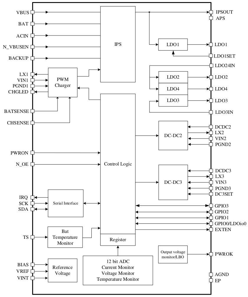
Their AXP20x products are highly-integrated PMICs that are optimized for applications requiring single-cell Li-battery (Li- Ion/Polymer) and multiple output DC-DC converters.and LDOs. Here is a block diagram:
![]()
The AXP20x features:
- A wide choice of input power source, the best source is chosen as IPSOUT inside the IPS (Intelligent Power Select) block :
- USB VBUS
- Battery BAT
- ACIN wall plug (not used in FunKey)
- BACKUP battery (not used in FunKey)
- A 1.8A fast PWM battery charger (also called DC/DC1) with battery voltage / current sense and programmable charge indication LED
- A soft key power-on/off logic with timer (just as in smartphones!)
- An I2C interface with interrupt signal to communicate with the CPU
- An optional battery temperature monitoring if the battery is equipped with an NTC resistor (not used in FunKey)
- A reference voltage
- A built-in 12-channel 12 bit ADC that measures various voltage and current data, as well as feeding an internal Coulomb counter and fuel gauge system (more on this later)
- A power OK output used to generate the global RESET signal in FunKey
- 5x GPIOs (not used in FunKey), GPIO0 can be programmed as LDO5 output
- 2x DC/DC SMPS DC-DC2 and DC-DC3
- 5x LDOs (only 2 are used in FunKey, LDO5 is optionnaly output to GPIO0)
Looking at their datasheets, it is difficult to tell the difference between the AXP202, AXP203 and AXP209 (any hint welcome!). In the FunKey design, we use an AXP209 because it is the one that comes along with the V3s when you buy it on AliExpress ;-)
AXP20x Application Diagram
For complex dedicated chips like this, the best option is to follow as much as possible the application diagram and reference design given by the manufacturer, as the internals of the chips are seldom fully disclosed, so you need to take their word on some of the external component values to use.
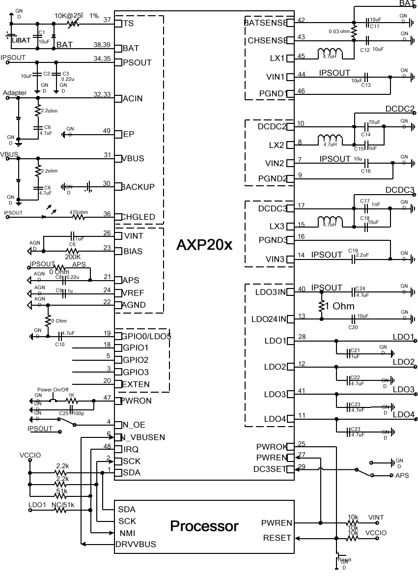
The Allwinner V3s Reference Design contains on page 6 the schematics for using an AXP203 to supply the power to a V3s-based dashboard camera design. It follows closely the reference designs provided in the AXP20x datasheets:
![]()
More hints are provided in my self-translated V3s Hardware Design Guide (page 7) too.
FunKey PMIC Design Adaptation
The FunKey device uses all AXP209 integrated SMPS:
- the PWM charger DC-DC1
- the DC-DC2 for providing the +1.25 V / 1.6A for the core
- the DC-DC3 for providing the +3.3V / 1.2A for I/Os
But compared to the sophisticated reference designs, the FunKey device only uses 2 out of the 5 integrated LDOs:
- LDO1 supplies the +3.3V / 30 mA Always On for the RTC
- LDO2 provides the +3.0V / 200 mA for the analog power supply
- LDO3 / LDO4 / LDO5 are not used by FunKey
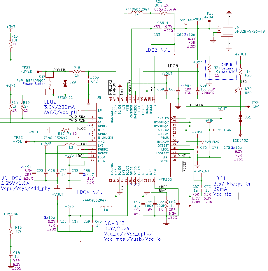
Here is the Funkey schematic block for the PMIC:
![]()
This schematic may look intimidating and complex, but it is in fact just a collection of simple basic elements, and it is actually very close to the manufacturer-recommended design.
The most noticeable difference is that the FunKey schematics use symbols and placement that are as close as possible to their corresponding physical package and layout, instead of defining symbols that are conveniently arranged by logical properties. Even if this makes schematics more complex at first sight, the benefit of this approach is that the step to go from the schematics to the physical layout become much easier, and so is the debugging of the physical board, which is then very close to the schematics too.
Another habit that is used everywhere in the FunKey schematics is that all signals (except power supplies and GND) are routed using explicit wires, rather than counting on invisible connection by net names and relying of the reader to search these names all over the place. This forces related components to be clustered in compact groups to shorten the wires, and put more focus on inter-cluster signals, with a natural inclination to unravel wire nests in the schematics before laying out the actual board.
And there are some "PWR_FLAG" symbols added here and there, which is the proper way in KiCAD to declare that a given net has a proper supply and thus prevent the ERC (Electrical Rule Check) to throw an error.
The end of this log details each PMIC function one by one:
Power Inputs (East side)
A wall-plug AC adapter input is not used in the FunKey device, so +VIN is just filtered using C75 on pins 32 and 33.
The USB power input +VUSB on pin 31 is filtered using C70, and the best (between +VUSB and +VBAT) available voltage is output to +VOUT on pins 34 and 35 and filtered using C78.
The BACKUP supply on pin 30 is not used and is left unconnected.
Internal Connections (All sides)
Some AXP20x signals are externally available and should be connected to external components:
- The +2.5V internal logic voltage VINT on pin 26 is filtered using the recommended value for C67
- The reference voltage VREF on pin 24 is decoupled with C64, and its BIAS connection on pin 23 is connected to a precision 200k 1% resistor R22, as recommended
Additionally, the AXP20x is actually made up of separate flexible blocks that require external interconnections to set their desired operation:
- All DC/DC inputs (VIN1 on pin 44, VIN2 on pin 7 and VIN3 on pin 14), as well as LDO3IN input on pin 40 are connected to the best available voltage +VOUT with filter capacitors C59, C23, C30, and C69, respectively
- LDO1SET on pin 27 is used to set the initial voltage of LDO1, and according to the datasheets, setting it to VINT sets its voltage to the desired +3.3V for the +3.3V Always On power supply
- OTOH, combined LDO 2 and 4 input LDOIN24 on pin 13 is instead connected to +3.3V in order to minimize the voltage drop for LDO2 to generate the +3.0V. Here too, there is a filter capacitor C34
- It is not clear what is the exact function of APS on pin 21 (it is described as "Internal Power Input"), but it is to be connected to +VOUT, too
DC-DC1 PWM Battery Charger (North East side)
The battery is connected to J5 (a 2-pin JST 1.0 mm pitch receptacle) and uses R21 as a precision current sense resistor, with C53/C56/C60 filter capacitors and L5 (a low-profile ferrite-core power inductor rated with a saturation current of 1.2A and low < 0.1 ohm resistance).
Please note that the battery is not protected on the board against reversing polarity, as the model used already contains a built-in protection.
R24 is mounted to simulate a battery NTC for measuring temperature, as the chosen LiPo battery does not feature this temperature sensor.
A user-programmable (through the I2C interface) charge LED D30 is provided, with its current-limiting resistor R26 (for which we need to raise the value as the LED is too bright!), as well as an TVS diode to prevent ESD, as the LED body will be accessible to to user.
DC-DC2 +1.25V / 1.6A (West side)
This SMPS is built around the ferrite core power inductor L3 and filter capacitors C26 and C29.
DC-DC3 +3.3V / 1.2A (South side)
This SMPS is built around the ferrite core power inductor L4 and filter capacitors C39 and C43.
LDO1 +3.3V Always On 30mA (South East side)
The LDO output on pin 28 is filtered with capacitor C72.
LDO2 +3.0V / 200mA (South West side)
The LDO output on pin 12 is filtered with capacitor C38.
LDO3 (North side)
This LDO is not used and its output on pin 41 is nevertheless filtered with a capacitor C63.
LDO4 (South West side)
This LDO is not used and its output on pin 11 is nevertheless filtered with a capacitor C38.
Power Key (North West side)
The AXP20x features a soft power key with internal short and long-press detection with user-programmable time settings, which enables turning power ON or OFF much like the way it is done in cellular phones.
Only a few external components are required: the tactile switch S13, its ESD protection TVS D29, and a low-pass filter R18 and C42 for debouncing the switch.
I2C Bus (North West side)
The AXP20x can be externally controlled by the main CPU using the I2C bus on pins 1 and 2. This bus has pull-up resistors to +3.3V R14 and R16, and the IRQ/WAKEUP signal on pin 48 enables warning or waking up the CPU on a selection of AXP20x-generated events, with a pull-up resistor R13 to +3.3V..
GPIOs (South and West sides)
GPIO0-3 on pins 19, 18, 5 and 3 are not used and are left unconnected.
PWROK (South West side)
The PWROK signal on pin 25 is used to generate the global RESET signal for the whole board, with a pull-up resistor R15 to the +3.3V Always On power supply.
Enable Signals (West side)
The global chip enable signal N_OE on pin 4 is always activated through a 2k resistor R17 to to GND.
The USB enable signal N_VBUSEN on pin 6 is directly tied to GND to always enable power from the USB bus.
Monitoring
Through the I2C bus and the numerous internal available registers, the AXP20x provides a very good control of its operation, including many threshold and timing settings, but also many voltage and curent monitoring values.
Coulomb Counters / Fuel Gauge
It is well known that battery discharge voltage curve over time is very flat, making it very difficult to estimate the real charge/discharge state of the battery. Moreover, these states will vary with temperature, load, and aging.
The only accurate way to monitor the battery status is to actually count the energy that is stored when charging, and the one that is consumed. This particularly important feature is achieved in the AXP20x using a dual Coulomb counter which continuously sums the current intensity over time for monitoring the battery accurate charge and discharge status, with user-defined alert thresholds.
This fuel gauge is providing the ability to precisely report the remaining battery capacity, just like people are used to with cellular phones.
FunKey project - All your games on your keychain !
Fun-on-a-Keychain is back, packing all your games and multiple emulators in a cute and extremely tiny handheld console.
 c.Invent