Andy
Andy-
Power-down of <1nA? with Just-in-Time Regulation
11/28/2020 at 12:35 • 0 commentsTL;DR
I took advantage of the ATmega1284p's wide operating supply voltage (e.g. 1.8v to 5.5v) and low power sleep state and developed something where the microcontroller can actually sip it's power-down supply current from an automatically rechargeable low-leakage on-board capacitor until more power is needed, effectively lowering the average power-down current *from the battery* to less than 1nA.
![]()
(Yes, that ATmega1284p is actually on and in power-down mode - video at the end of the log.)
Part One
Phew. Was that really a TL;DR?!
Those following along will remember the above photo from the end of the last project log.
And yes, that ATmega1284p on one of my Pro Mini XL (v2) boards really is "on" and in power-down mode.
Don't believe me? Let's wake it up then by grounding INT0...
![]()
See the LED light up despite drawing less than 1nA? It's alive alright!
So what's going on?!
Well...
Have you ever noticed that after you disconnect power from some devices, they remain on for a little while?
See that power LED on your phone/laptop charger slowly fading off in to the abyss of nothingness?
There can be a number of reasons for this.
But the one that interested me recently was that of the remaining charge stored in the on-board capacitances.
On-board decoupling capacitors, for example, for the ATmega1284p are typically 100nF, maybe an additional 1µF thrown in there too.
You might also have a 10µF sat on the output of your boost converter or LDO!
It occurred to me that all those capacitances are just energy stores that a powered-down microcontroller could be happily sipping.
If it's powered-down state was low enough, say, less than 1µA...
So long as the voltage this capacitance supplies doesn't fall below the microcontroller's minimum, well, why not make use of it?!
But how to stop it from eventually falling below that minimum?
Why, with some nanoamp-sipping intelligence to periodically measure the supply voltage available and recharge the capacitor(s) up again - but only when necessary!
The charge level could then be configurably and/or programmatically set (even by the microcontroller itself!) and then this new supply voltage system - a sort of "Just-in-Time" Regulator - could be forgotten about when powered-down.
And that's exactly what the video below demonstrates.
There are no huge electrolytics hiding in there, just the ordinary capacitances associated with a regulator and decoupling.
But you could, of course, add one if you wanted to extend maximum potential power-down period.
I've set the "regulated" maximum and minimum to 5v and 1.8v respectively, and am using a switchable boost converter to get 5v from those two AA batteries - that's why the in-rush current is in mA.
I'll update this log with more details about what's going on in the video, probably on Monday.
But I've been able to successfully power additional nA circuitry, for example, custom battery measurement, real-time clocks and sensors from this just-in-time regulator (JiTR?) all without too much impact on the maximum potential power-down period.
More details on all that soon!
And again, thanks to various awesome Internet folk and resources including Nick Gammon, Jean-Claude Wippler (JeeLabs), Charles Hallard (ch2i), Pascal Moreau (MySensors) and others - you all helped make this possible.
-
How Low Can It Go? Pro Mini XL and nA Power-Down
11/27/2020 at 18:17 • 0 commentsTL;DR
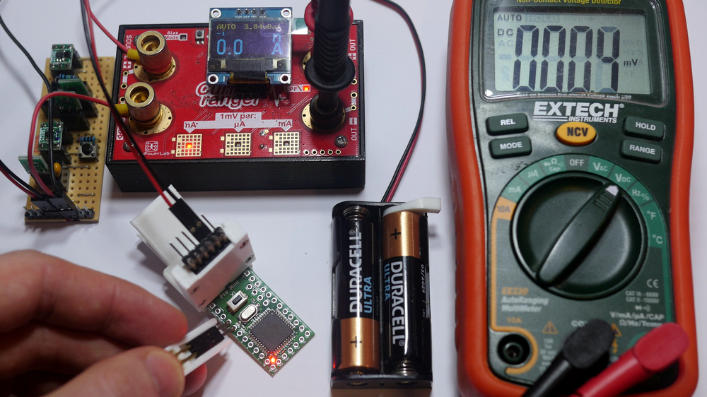
I got the Pro Mini XL (v2) to power-down below 100nA and still wake up from an external interrupt - photos, video and code below.
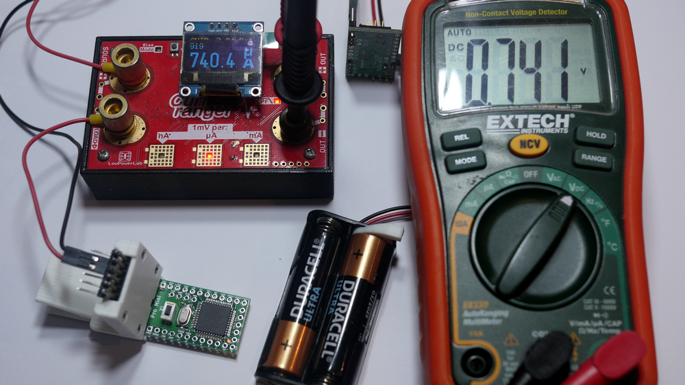
Your mileage may vary (YMMV) because the ATmega1284p is only spec-ed to power-down at 150nA from 1.8v in the datasheet, but here's the proof some of their chips can operate lower:
![]()
In More Detail
In the photo above the Pro Mini XL (v2) has been fused to run at 1 MHz with it's Brown-out Detection (BoD) turned off - allowing it to operate, seemingly happily from a fresh 1.5v AAA battery.
The video below shows it first powering up, doing a bit of low-power housekeeping and then powering-down to less than 100nA:
Board pin 2 (INT0) had been configured as an active-low wake-up interrupt and so when I ground it, you can see that the board springs to life again, before powering back down.
The code (available here) would actually light the on-board LED if the forward voltage was high enough, sadly 1.5v won't cut it so it appears off.
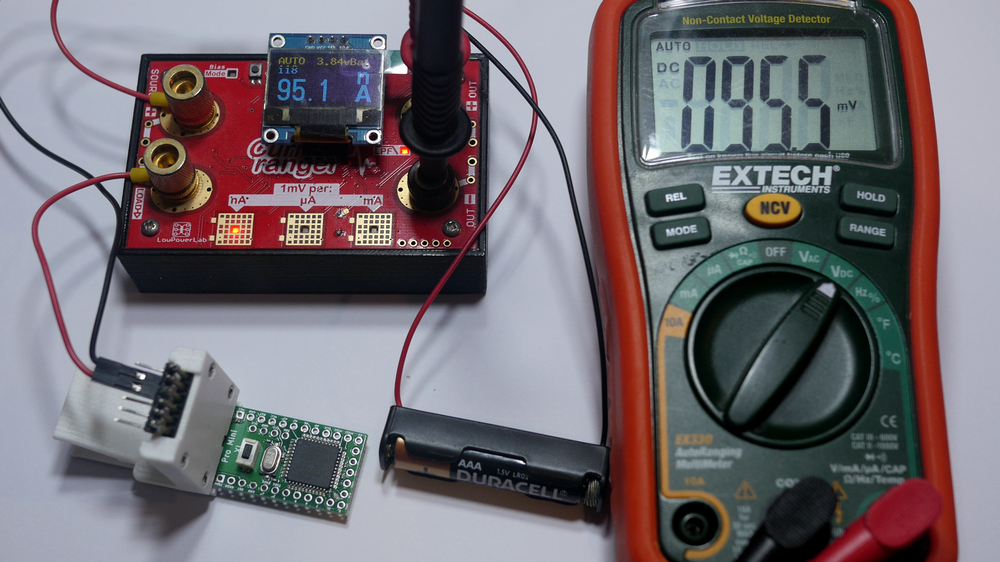
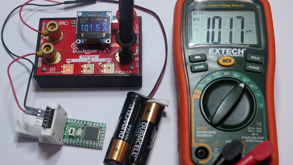
But the photos and video below shows the same board, same code just with a regulated 1.8v supply drawing roughly 1nA more whilst in power-down and the "proof-of-life" LED being lit (bottom corner) when it's awake.
![]()
![]()
It's awake - honest!
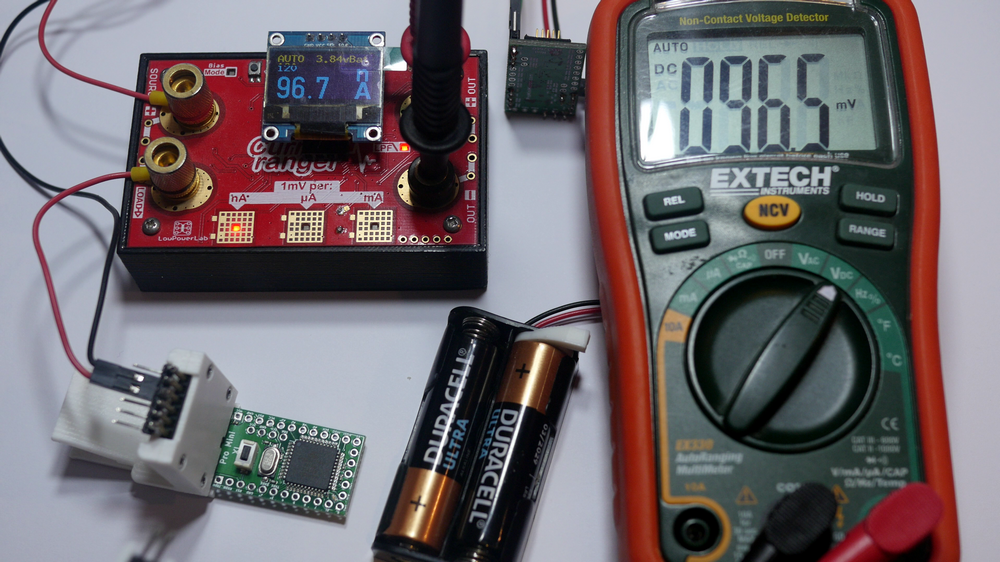
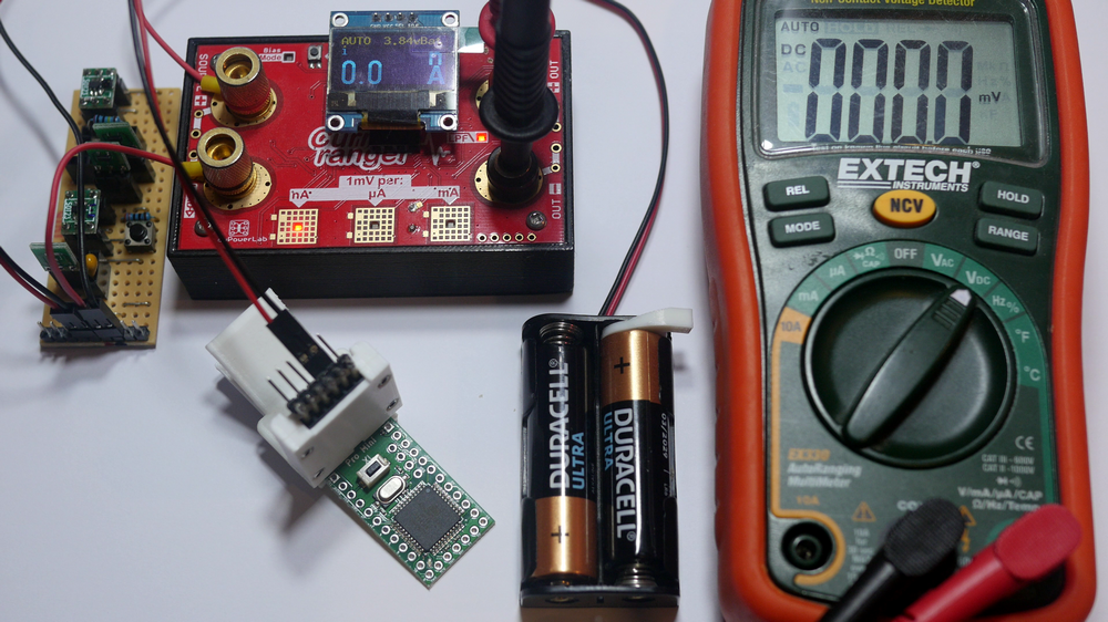
And by way of comparison at 3v, running directly from those two AA batteries, it just peaks over 100nA:
![]()
Again, same board, same code - just varying the supply voltage:
Now...
Thanks to various awesome Internet folk and resources including Nick Gammon, Jean-Claude Wippler (JeeLabs), Charles Hallard (ch2i), Pascal Moreau (MySensors) and others, I've also been developing something that enables any Pro Mini to draw these few nA from an automatically topped-up "storage" - a sort of "just-in-time" regulator - cutting the power-down battery draw to basically zero.
I'll write more about it soon, but here's a photo and video (to follow) to whet your appetite:
![]()
Believe it or not, in the above photo, the board is actually in power-down and can happily remain there for a configurable amount of time.
Again, same board, same code, but watch what happens when I trigger the interrupt...
![]()
See the LED light up at the bottom corner of the board - it's alive!
I'll update this log with more details soon!
-
No Pain, Just Memory Gain:Using the Pro Mini XL with The Things Network
07/04/2019 at 00:38 • 0 commentsTL;DR
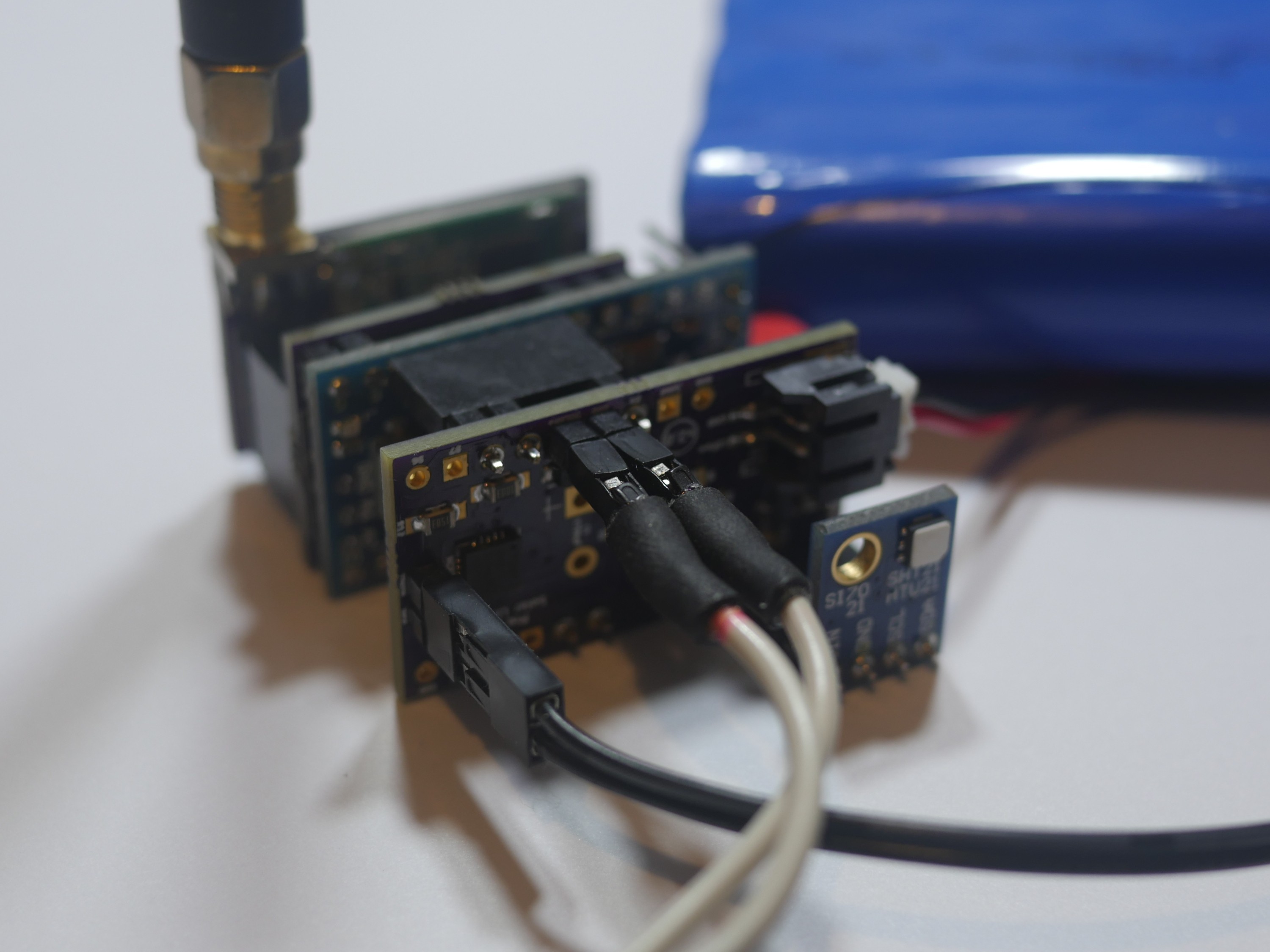
I got the Pro Mini XL working with the Arduino-LMIC library. It’s performing OTAA to The Things Network over LoRaWAN. And it’s reporting temperature and humidity measurements from an SI7021 sensor - with 80% program memory to spare!
![]()
(Note: There’s no SI7021 sensor connected in the central photo - I added it in later when my extra female pin headers finally arrived!)
In Brief
I’ve been running out of memory.
Whilst trying to develop/debug a Pro Mini 328P-based low-power temperature/humidity sensor node on The Things Network over LoRaWAN, I’ve been reaching the 32KB program memory limit and 2KB dynamic memory (SRAM) limit.
Then it occurred to me.
Why not test the pin-compatible, drop-in replacement benefit of the Pro Mini XL?
Essentially, all I needed was more program memory and SRAM.
So I updated the pin-mappings, replaced the 328P for the XL, recompiled.
Shazam!
Everything just worked!
And now my existing Arduino sketch was only using 20% of the program memory!
Now to add more sensors: GPS. Altimeter. Barometer.
Hmmm, what else could I fit, I wonder...?!
Gettng Started
I began tinkering with all things LoRaWAN back in 2016 during a commercial farm monitoring project.
Farmer "Dave" needed to monitor the temperature and humidity of a 120+ acre farm.
But it was approx. half an hour’s drive away from the main HQ.
Initial research into low-power, long range radio transceivers led me to LoRa and LoRaWAN.
I soon discovered that I had just missed out on a Kickstarter campaign for The Things Network (back in 2016), but I pre-ordered myself a Gateway, Node and Uno anyway.
Whilst I waited for the official development devices to arrive, I did what any impatient "Tech Tinkerer" would do...
I DIYed my own.
Using a Raspberry Pi 2 and LoRa concentrator board for the gateway (more on that below!) and a nice supply of Pro Mini 328P clones with Hope RFM95 radio modules for the nodes, I was all set.
So I set up a LoRaWAN system of solar/battery powered nodes and a gateway to provide the environment visibility Farmer "Dave" needed.
All was ticking along nicely.
Until one day a blaze of fire consumed one of the barns and almost all of the tech perched on top of it! (Thankfully, no one was injured and the fire was contained quickly.)
So I was invited back to upgrade and reinstall a new one.
The (Main) Problem
In a word: freezing.
Farmer "Dave’s" farm sits at over 4,000 feet up in the mountains, so it gets cold.
Very cold.
Especially at night.
It can get so cold that it will freeze the fruit buds when they’re just starting to emerge… and then that’s it.
Your entire crop is gone - for another year!
So how to stop the buds from freezing?
You can only resort to defensive measures (e.g. water sprinklers, etc.) when you’re almost positive a freeze is imminent.
That's because it might actually cost tens of thousands of dollars to do so.
Especially in a state with severe drought like California.
In a perfect world you would monitor as much about the local environment as possible to help you predict when freezing might occur.
Temperature, humidity, altitude, barometric pressure, wind speed, etc. all play a factor to a greater or lesser degree.
You might also want some sort of location information from a GPS perhaps, to tie all that environment information to a specific area.
On large scale farming, you could get micro-climates specific to one area of a field that differ from another area - depending upon the geography and topology.
However, using the Pro Mini 328P as the microcontroller for the LoRaWAN nodes had previously constrained the number of sensors I could comfortably hang off it.
With only 32KB program memory, I ended up limiting myself to an SI7021 to monitor temperature and humidity.
But now I was revisiting the problem with my freshly minted Pro Mini XLs.
I wanted to see how easily I could replace the existing Pro Mini 328Ps and how much room I would have for anything (...or everything!) else.
So I dug out a breadboard, Pro Mini 328P clone and radio module and set to work.
Testbench Tangents
Initially, I breadboarded everything in the usual way.
And of course, wires were sticking out everywhere like a rat’s nest.
Debugging bad connections on the breadboard soon began to eat up precious time.
So I decided to make a strip-board testbench instead with female headers for the microcontroller.
In theory, this would enable a more repeatable like-for-like comparison when I later compared the different Pro Minis.
I wanted to test whether I could literally just swap out the 328P-based Pro Mini for my Pro Mini XL, and even possibly the Pro Mini nRF52.
Since I was also going to make an upcoming move between the continents (UK to US...and back!) and needed to respect the frequency changes (e.g. 868 to 915 MHz) in the LoRaWAN spectrum, I also added female headers for the radio module too.
Of course everything needed a common power source, but I wanted to see first if I could get away without using a regulator and run direct from a battery.
So I went with two male header pins and a standard 3v supply from two fresh 1.5v AA Duracell batteries.
And last, but by no means least, was debugging over the UART.
Three more male header pins for GND, TX and RX connecting the side UART pins of the Pro Mini boards.
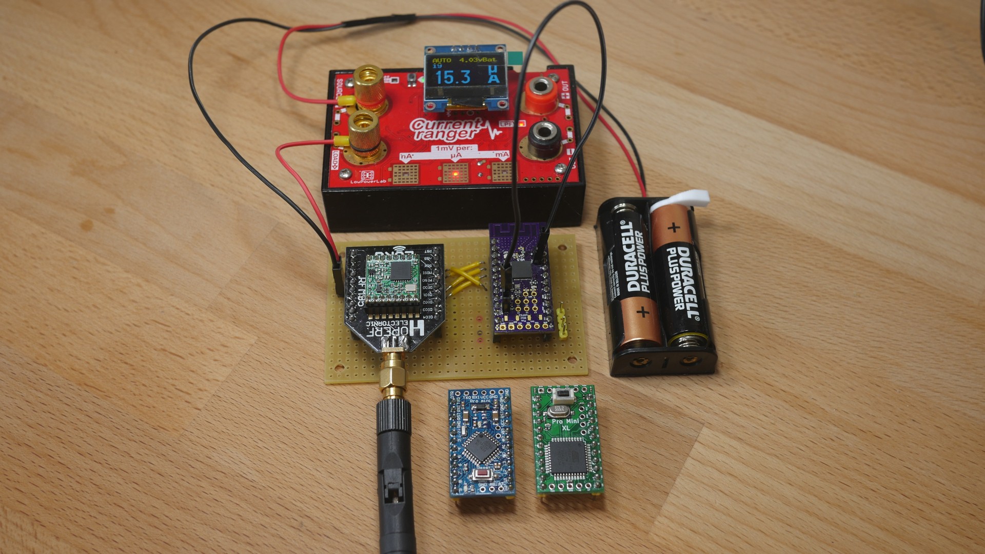
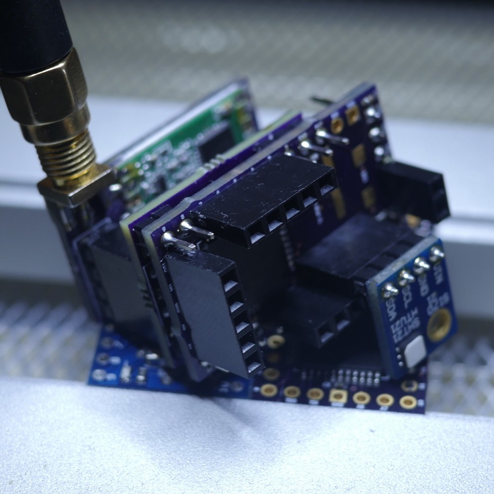
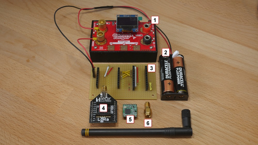
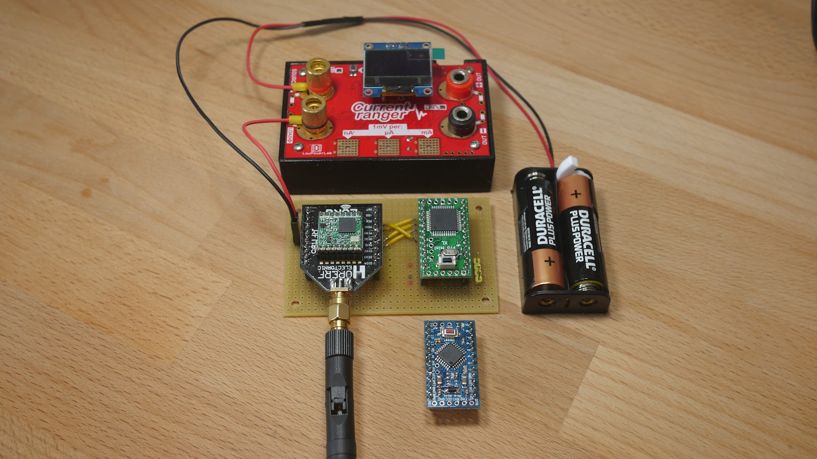
This is what all of the above looked like:
![]()
- CurrentRanger with OLED Display
- 2x AA Batteries with 3D Printed Cam-Switch
- 80mm x 50mm Strip Board with various wires and 2.54mm Male/Female Header Strips
- GorillaBuilderz LoRa Adapter PCB for RFM95 Modules
- HopeRF RFM95W LoRa Module (Only 868 MHz Shown)
- 868 MHz Antenna with SMA Male-to-Female Adapter (Can't remember where I bought this...)
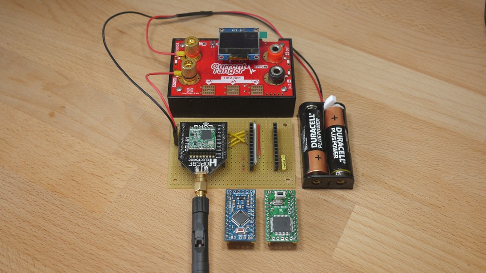
And here it is again with the radio module plugged in and (almost) ready to go:
![]()
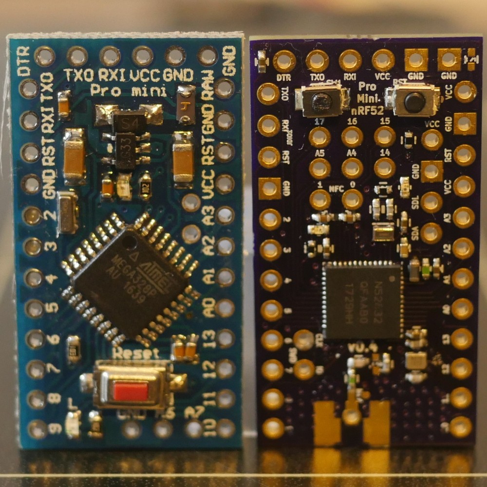
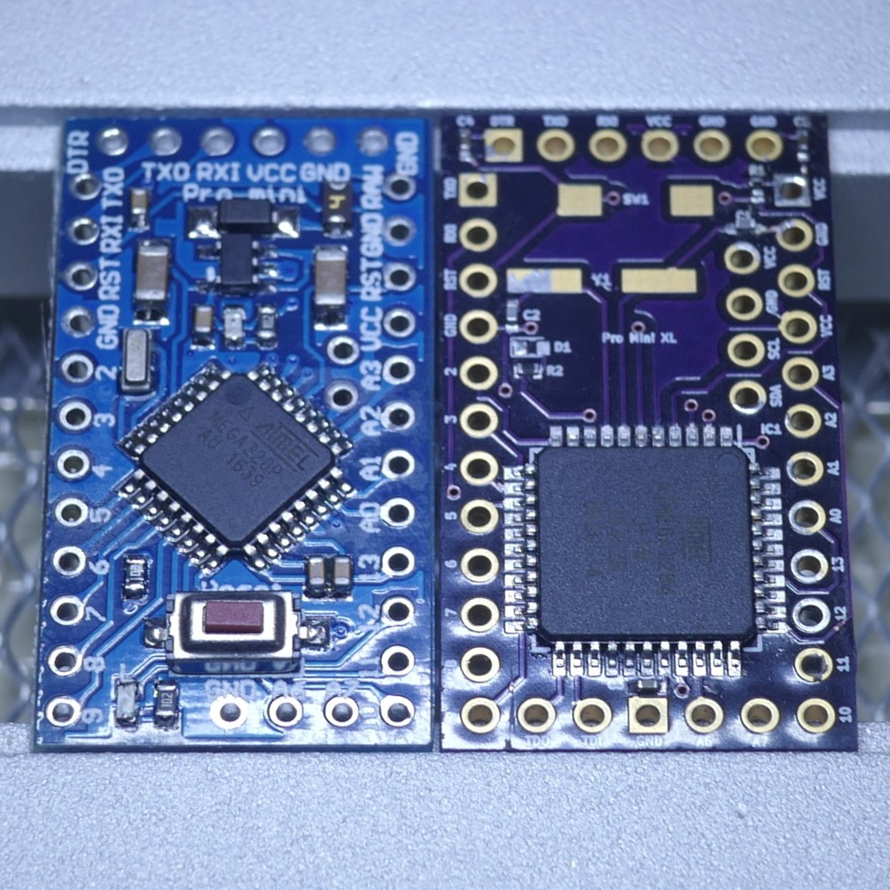
(Note: Pro Mini 328P on the left in blue, Pro Mini XL with ATmega1284P on the right in green.)
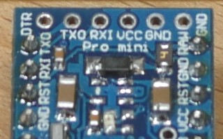
Low Power Mods
The (very) eagle-eyed among you will notice some components missing from the Pro Mini 328P.
And you’d be right:
![]()
You’ve probably seen mods like this to reduce the power consumption of the standard Pro Mini 328P.
My initial reference for this idea was this one from back in April 2013.
Patrik had removed the regulator and power LED from his 5v, 16MHz Pro Mini 328P board and reduced his overall average current down from 476uA to 136uA.
Quite a saving!
In the same manner, Andreas had modified the same kind of Pro Mini 328P clone as I was using and had further profiled the power consumption of just the sleeping microcontroller down to 20.9uA.
If you’d like to learn more about power saving techniques for microcontrollers like this, then I highly recommend Nick Gammon’s lengthy but awesome posts on the topic from back in 2012.
Possibly the genesis for the above experiments? I don't know...
In my case, instead of removing the power LED, I simply removed the 1K resistor next to it accomplishing essentially the same thing.
I’ve found 0603 SMD LEDs a bit tricky to remove without damaging, especially using either hot air or soldering iron.
Removing the 1K resistor instead meant that I could always restore previous function later if I needed - since 1K 0603s are practically ubiquitous.
Nothing unique about this variation-on-a-theme, but I hope maybe helpful to the unfamiliar.
The voltage regulator, by comparison, came off with copious amounts of flux, wicking and tightly directed hot air.
Wiring Connections
Wiring connections between the microcontroller and radio were straightforward.
SPI connections are standard pin-to-pin, as are VCC and GND.
I took advantage of pin and track alignment on the strip board to connect DIO0 and DIO1 from the radio module to A2 and A3 respectively and finally wired RST to A0.
[Insert Wiring Diagram - I'll try to do this when I get a moment...]
You'll see the pin mappings in the Arduino code below too.
A DIY LoRa Gateway
All well and good, but at this point all I’ve made here is a (potential) LoRaWAN Node.
What about the LoRaWAN Gateway you ask?
After all, what is going to receive and forward all these LoRaWAN packets to The Things Network?
I couldn’t use my pre-ordered (and now delivered!) gateway from The Things Network, since I had subsequently deployed that elsewhere for another project.
And I couldn’t afford to buy another just yet at this phase of development.
So I had to improvise…
Behold:
[Insert Photo - Still need to photograph this one...]
This is very much a DIY set-up right here - but it works!
[Note: If you're not really interested in all this LoRa Gateway stuff, please skip ahead to 'The Baseline' section below, since I go off on a bit of a tangent here...]
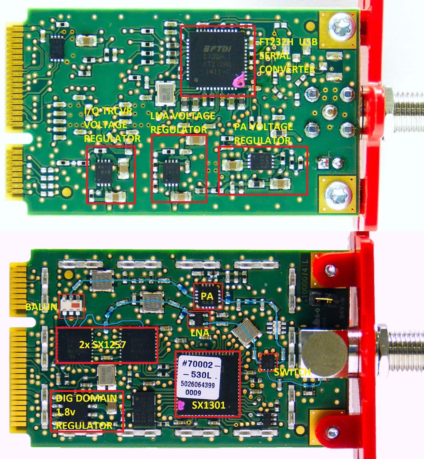
Basically, I’ve got a Raspberry Pi 2 with one of Multitech’s (old) LoRa mCards inserted into a modded USB-to-Mini-PCIe converter.
I actually made this back in 2015 from Nestor’s fantastic wiki guide right here.
He really deserves all the credit for reverse engineering Multitech’s hardware and getting a software solution working.
Essentially, you’ve got a triplet of Semtech LoRa chips (1x SX1301, 2x SX1257) interfacing via SPI to a standard FT232H configured in USB-to-SPI mode in what (I understand) was quite a common LoRa “Concentrator” design at the time.
Nestor’s hardware modification is simply to power the mCard from the RPi 2’s 5v supply and interface.
You’ll probably need to remove the RPi 2’s built-in (software) current limiter to get the concentrator to start up correctly (like Nestor demonstrates below) or power it externally.
![]()
On the software side, it was less straightforward.
Nestor needed to configure the original lora_gateway code to use a different FTDI USB to SPI converter PID, reset the SX1301 by toggling one of the FT232H's GPIO pins and finally trace the right clock source from the SX1257s to the SX1301.
Phew!
Again, the details are in the excellent wiki and all I did this time around was reconnect my original hardware and update/re-compile/execute the software from Nestor’s git.
And everything just worked. (Thank you Nestor!)
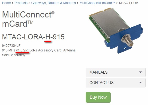
Sadly, Multitech discontinued the original LoRa mCard used in the above tutorial and replaced it with a new SPI only version in 2017 - i.e. no USB to SPI (through FTDI) bridging anymore.
Therefore, the new hardware is NO LONGER compatible with Nestor’s tutorial.
However, it might be possible to still get it working by applying some patches from here.
Take a look at the “lora-gateway-usb” and “lora--packet-forwarder-usb” patches in particular.
I’ve not looked into this myself since I don’t possess the new SPI-only mCard, so I’m afraid I can’t assure you of any success - sorry!
There are lots of other LoRaWAN Gateway cards in this mPCIe format though as well as standalone boards, modules, devices and, of course, The Things Network’s own offerings.
Personally, I think the next time I take a look at this, I might try building Will’s OpenSource version!
It looks awesome and is designed to be in a Raspberry Pi hat format.
Although it can’t current do LBT (see below) - take note Korea!
So take your pick, but back to the Multitech tangent...
Old vs. New Hardware
The reasons for Multitech upgrading their mCard were probably many.
Here’s my guess at a few of them - please correct me if I’m wrong!
First, the original LoRa mCard and associated software implemented what looked to my eyes to be a very basic downlink queue - “very basic” as in a queue depth of 1.
Yeah...
Basically, any downlink packets sent to the gateway were either immediately sent out or risked being overwritten by any subsequent downlink packets.
One option to delay the inevitable was to increase the RX delay to, say, 5-8 seconds or so which might allow sufficient time for the downlink message to be received and pushed to the packet forwarder before another came along.
But as you can imagine, it wasn’t a solution.
I understand that Semtech subsequently released a version of the packet forwarder that implemented a basic software queuing structure.
But in the end even they decided to deprecate support for FTDI in version 2.2.0.
Moving to a purely SPI-version of interfacing with all the SX chips provides the most flexible approach to queuing and inter-chip communication anyhow.
FPGAs and LBT
Second, Semtech’s AP2 reference design for their SX1301/8 chips calls for an FPGA to implement the Listen Before Talk (LBT) feature in spec. v1.5.
The idea behind this feature is to make it at least possible for multiple transmitting nodes to share the same transmitting channel.
Nodes would continuously monitor the channel(s) to determine which channel(s) are free and when, and then only transmit when a channel is not in use by any other node.
Semtech’s recommended implementation calls for an FPGA chip, like the iCE5LP2K that Multitech use in their updated mCard:
Thermal Solutions
Looking at the backside (see below) of Multitech’s updated mCard, suggests that the new version might have a better heat dissipation profile too.
The original version had the FT232H on (almost) the exact opposite side of the SX1301 - see the above board layout.
Under load, the metal cover on my DIY gateway would become too hot to touch and, under heavy load, felt like I could fry an egg on it!
The Things Network guys in Leiden went with a passive heatsink…
...a very big heatsink!
Since the new version uses SPI only, there is room on the backside of the SX1301 for a heat dissipation pad.
My gateways tended to become unpredictably unreliable (worst of both worlds) when they got too hot - and I don’t think I was the only one.
Better cooling always made the “problem” disappear, so hopefully this improved board layout and chip placement will go some way to mitigate that issue somewhat.
The Baseline
Now that all those testbench tangents were out of the way, I moved on to (re)establishing some baseline results with the original Pro Mini 328P.
Whenever I revisit a past project, I invariably spend half a day getting back to where I left off.
It can be painful.
But it’s usually always profitable too.
Improved Uploading
The first profitable improvement I made - that I think is worth mentioning here - is updating the standard Pro Mini Optiboot bootloader to run UART0 at 250Kbps for uploading.
Why?
Well for one, it’s faster at uploading code.
Your typical Pro Mini 328P will often come with a bootloader running at either 38.4Kbps, 57.6Kbps or at the most 115.2Kbps.
But these are simply a standard practice.
Buried deep in the recesses of the ATmega 328P datasheet, on pages 196 to 199 (of 662!), you see tables showing (among other things) how UART speed, microcontroller frequency and error rate compare.
Notice that when running the microcontroller at a frequency of 8 MHz and the UART at a baud rate 250KBps the error rate is still 0%.
In fact, you’ll notice it’s still 0% right up to 1Mbps!
So why not run it at 1Mbps?
Well, I might, given a specific scenario, but at least at 250Kbps, I can run the Pro Mini at 2, 4, 8, 16 and even 20 MHz - see the other tables.
I ran a few initial tests and uploading was solidly reliable.
Again, this idea isn’t original to me.
The first person I read about who’d pulled it off was Charles Hallard with his awesome ULPNodes.
Charles designs great boards and I’ve bought his stuff before, everything from WeMOS gateways to NodeMCU gateways.
(Check out his new one that uses a TPL5110 as a power gate and has written his own bootloader to boot!)
Improved Sketch
The second improvement I made was to re-write my basic wake-on-interrupt sketch.
I wanted to see just how much I could successfully hang off the Pro Mini XL.
But at the same time, I wanted to easily use the same sketch for both the Pro Mini 328P and Pro Mini XL.
That meant being able to configure which peripherals were attached to testbench.
Enter the #define.
For the unfamiliar, wrapping code sections with #ifdef and #endif allows the compiler to ignore whole sections of your code if a #define is not present.
So in the screenshot above, if line #33 (#define SENSOR_SI7021) was commented out or not present at all, the compiler would simply ignore lines 40-56.
This was the first time I’d intentionally used them as a way of making “configurable” code to be used in a sort of “cross-platform” way and it worked quite well.
Please see my Github project for a repository of the code I used during this project log.
Results: Pro Mini 328P
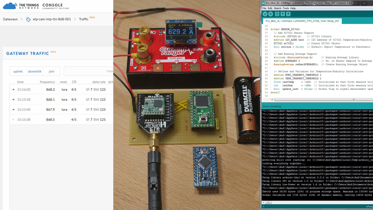
With everything compiled and uploaded, I fired up the CurrentRanger and watched…
In short, the video shows the microcontroller booting up, joining TTN and dropping into low power wake-on-interrupt sleep.
I then short the interrupt pin to wake it, whereupon it sends another data payload and drops back into sleep.
Nothing fancy.
Just a proof-of-concept to give you an idea of the general code size required to accomplish a basic node operation.
But look how much of the program memory on the Pro Mini 328P it uses up:
This (very) basic sketch uses up 76% of the available program memory and uses a further 81% of the available dynamic memory (SRAM).
That doesn’t leave much for adding more sensors or a GPS - not to mention simply expanding the main code beyond this basic operation of wake-send-sleep.
In fact, even just increasing the LMiC debug verbosity by one level in the existing libraries, i.e. no new sensors, etc. just the LMiC and SI7021, blew through the Pro Mini 328P's SRAM completely:
![]()
But back to the original compile above, it is also worth noting the red warning message there too:
![]()
As your code size creeps ever closer to the maximum available in your microcontroller, stability issues start to rear their ugly heads!
Your code might run fine initially, then appear to lock up or reset the microcontroller for no apparent reason.
Not great when you’re trying to protect 120+ acres of fruit farm from a crop-threatening freeze!
Or some other security or safety sensitive operation.
So what can you do?
At this point, I would usually turn to Bill Earl’s excellent Adafruit article “You know you have a memory problem when…” to harvest what was low-hanging.
See especially the section on Solving Memory Problems where Bill deftly breaks down some helpful tips and tricks on how to optimize program memory, SRAM and make better use of EEPROM.
Not this time though; I needed to “earn more”, not try to “save my memory rich”.
But how straightforward would that be…?
Results: Pro Mini XL
I took one of my Pro Mini XLs and set it up as close as I cared to mirror the 328P.
I set it’s fuses to use the internal 8 MHz oscillator, uploaded an Optiboot bootloader to use UART0 at 250Kpbs and swapped it for the 328P in the testbench.
Then I literally took the same wake-on-interrupt sketch and just changed the pin-mappings to those of the Pro Mini XL.
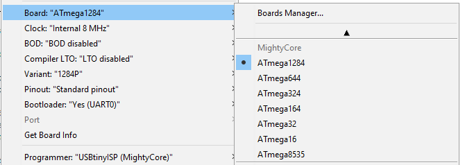
Finally, I needed to add the ATmega1284P as a new compile target in the boards menu.
Although this was a multistep process, it was also a straightforward one which I detail in the “Getting Started Guide” for the Pro Mini XL.
You add another Board Manager URL, download through the Board Manager window and then select the newly added Board options.
![]()
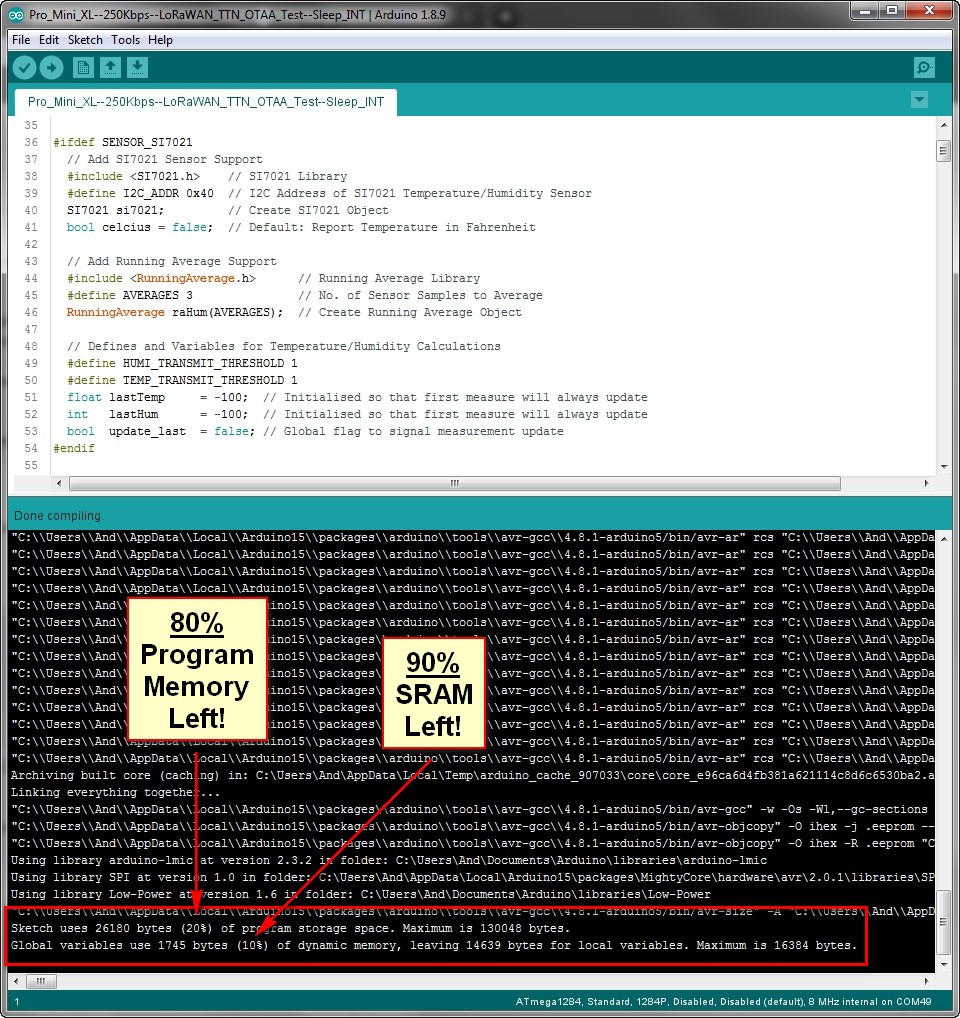
So with the new target selected, I re-compiled, uploaded and this is what I saw:
![]()
Yes, you read that right.
The same sketch uses up only 20% of the available program memory and only 10% of the available SRAM!
I now had almost 100KB more still to play with - more than 3x ALL the program memory of the original 328P.
But did the same code still run as before?
See for yourself:
The microcontroller boots up, joins TTN and drops into low power wake-on-interrupt sleep.
I then short the interrupt pin to wake it, whereupon it sends another data payload and drops back into sleep.
Exactly the same.
And that’s the point!
The Pro Mini XL proved its purpose as being a drop-in replacement for the original 328P.
I only needed more program memory and SRAM and that's exactly what I got.
With the bare minimum of fuss and effort on my part.
No code optimization.
No library modification.
No bootloader shrinking.
Just more memory.
Having said that, the more observant among you will have noticed the slightly lower power consumption during sleep at approx. 630nA.
I’m not entirely sure why that is, but during testing it did appear to be consistently lower.
Epilogue
This log entry was an attempt to cover my journey as I revisited an old project and did something new.
By using the Pro Mini XL, I was able to solve my previous memory problems without creating any new ones.
And the beauty of this board is that it’s also pin compatible, so I can replace the 328Ps in my other nodes without having to make any further modifications.
The reduced sleep current at least appears to be a nice bonus too!
Finally, a MASSIVE THANK YOU is definitely in order!
Any hardware is only as useful as the software makes it to be.
The only reason why any of this "just worked" is down to the awesome effort of everyone involved with the software and libraries.
I'm afraid I'll have to avoid naming individual names, since I'll inevitably leave someone out, but in an attempt to cover my bases:
A MASSIVE THANK YOU to everyone who helped shape the MightyCore Library into what it is today.
Thanks to everyone who helped get the 1284P core working with Arduino.
Thanks to everyone who helped with the underlying core code, supporting libraries, bug fixes, etc.
This project would not have been a success without you!
One Last Thing...
Curiosity, got the better of me.
Would the Pro Mini nRF52 work just as well?
After all, it's pin-compatible too and has 16x the program memory of the 328P.
To cut an already far too long story short, it certainly appears to...
![]()
If you'd like to hear more about that, please let me know in the comments section below.
Also, any other questions, comments or suggestions - I'd really appreciate hearing from you.
Thanks!
-
Benefits or Limitations: The ATmega 328p Pro Mini
04/26/2019 at 11:33 • 0 comments"Any benefit can become a limitation."
(Anonymous)I’m sure you’re all pretty familiar with the ubiquitous Pro Mini.
Or at least, this guy, his cheap (~$2) counterfeit cousin!
Based around the ATmega 328p, the “trusty” Pro Mini quickly became a feature of many of my DIY electronic projects.
There wasn’t a sensor or actuator I couldn’t connect to it via some sort of associated circuitry.
And then there were the libraries!
Awesome people around the world had written code to interact with almost anything and everything else.
But that was sometimes where I would hit my first limitation.
32KB Program Memory
Over the years, feature-creep™ has resulted in some of my projects pushing the limits of the 328p’s 32KB program memory.
For example, pan/tilt stepper solar-powered sun-tracking long-range wireless over-the-air programmable crop monitor...with camera and display anyone?! ;p
Once I started stacking libraries, adding features and increasing the number of external entities I was interacting with, my compiled code size (understandably) started to balloon.
Sketches that would get too far above 90% of the program memory fell prey to memory leaks.
Others would, of course, simply exceed the compiled 32KB limit altogether.
At first, I would attempt to fix the memory leaks, then it was optimize the code, add #IFDEFs to debugging portions and finally play with compiler flags.
If you’re wondering at this point whether all this effort was worth it, well, quite frankly so was I!
Learning to write better code is great.
But I could see the other members of the ATmega family of microcontrollers like the 2560, 1284p (and even the 644p) glittering off in the distance like so much fool’s gold.
[To be continued with…]
No Built-in Wireless
The Need for Speed
Running Out of GPIOs
Fixed Pin Position Interfaces
That Regulator & Power LED
Why Pin-Compatible?
Why Size-Compatible?
-
32-Bit & Wireless: The Pro Mini nRF52
04/25/2019 at 14:07 • 0 comments![]()
Above: Pro Mini nRF52 (right) shown next to a Pro Mini 328p clone (left).
(Note: An early development Pro Mini nRF52 shown with edge SMA, through-hole and U.Fl antenna pads.)
In the beginning
Shortly after the Pro Mini XL was born, I could feel the 32-bit world calling with its technological siren song.
Microcontrollers in this space boasted faster speeds, even more program memory, DMA, etc.
All very enticing for solving my Pro Mini problems.
One of the realizations I came to after creating the Pro Mini XL, was that I was obviously still board-stacking.
Many of my more recent projects had gone wireless, especially in the area of Home Automation.
I found myself adding nRF24s, RFM69s, 95s or RN2903s to get the range and/or protocols I needed.
And then there was encryption, “uniquification”, and over-the-air updates.
I had boards with ATSHAs, EUIs and additional SPI Flash amongst other things.
Add power distribution, monitoring, battery charging and actuators and we’re already at a 5+ board stack!
![]()
So I took the 32-bit world’s red pill (or rather “Blue Pill”) and began to explore.
I decided to focus my initial efforts on 32-bit microcontrollers that had built-in radios that I was already using.
This lead to the natural selection of Nordic’s nRF52832.
Benefits
The nRF52832 is a 64MHz ARM Cortex M4 CPU (with FPU), 512KB flash (!) and a built-in 2.4GHz transceiver.
The transceiver also supported Bluetooth 5, Bluetooth Mesh and ANT - which all sounded interesting.
Scratch one radio board from my stack.
Just as interesting was 128-bit AES/ECB/CCM/AAR (for encryption), 64KB RAM and 32 configurable GPIOs.
Scratch at least one more board from my stack.
All of this board-scratching sent me ferritting about for how to best get my hands probes on one.
What confronted me was a veritable sea of modules and dev. kits, many of which were breadboard hostile.
Most of the modules I saw had castellated pads requiring mounting to another PCB before use in my stack.
A Pro Mini-sized board only leaves approx. 13mm between the right and left hand side edge pins.
Modules that had metal shielding (for FCC certification, etc.) were simply too wide.
Did I care about metal shielding or FCC certification? At this point, no - I just wanted something to play with.
So all the modules were either too wide to fit between the pins or I was going to be looking at some sort of oversized mounting PCB with 2.54mm SMD pin headers.
Other dev. boards in the line up that were 2.54mm pin-friendlies like Adafruit’s Bluefruit or SparkFun’s Dev. Board weren’t Pro Mini pin-compatible.
They made up a sea of different pin-out and board layouts
All-in-all, rather non-friendly to an 8-bit Pro Mini native seeking his fortune in the 32-bit land of opportunity!
So, I decided to roll my own.
Limitations
Since the nRF52832 was available in a QFN-48 package, this gave me more routing room than the 1284p.
But I’d never worked with a QFN package like that before and didn’t know whether my “skillz” were up to it.
Not one to shy away from a challenge though, I sketched out Nordic’s reference circuit schematic and began.
I opted for the extra DCDC componentry to enable some lower power operations for later experimentation.
After a rough place-and-route, the essentials fit quite nicely between my self-imposed prison of Pro Mini pins.
However, the question then became, what exactly to route out, and where to?
SWD vs. FTDI
First on the list were the SWD programming pins.
I had very limited JTAG/SWD experience coming, as I did, from the FTDI-world of the 8-bit ATmega.
So my first thought was whether there was some sort of half-way house to ease my transition.
Nordic’s SDK for the nRF52832 described a bootloader that could update the firmware of the device via UART.
That sounded ideal.
The device simply needed to be “reset” into a state in which it would patiently wait for new firmware.
SparkFun had accomplished this via Nordic’s recommended combination button press.
On the other hand, Adafruit had also added some componentry to their FTDI DTR pin to simulate the reset button press and a brief wait (~1.5s) for any new firmware on every reboot.
You could force a longer wait using the same combination button press on their board too.
I liked the idea of being able to still use my small army of FTDI programmers and their associated Fiddy’s.
As well as knowing that some project boards relied upon the position of the Pro Mini’s FTDI pins for TXD/RXD and/or VCC and GND.
So I threw two small push buttons, FTDI pins and a resistor/capacitor pair onto my fledgling 32-bit Pro Mini board.
Since sprinkling two LEDs into the mix would make identifying the bootloader state a little easier, these went on too.
I also made sure to route the SWD CLK and IO pins, since I would need access to these anyway to put the custom bootloader on in the first place.
There was no escaping learning to (re-)program in the 32-bit MCU world.
At the time, I thought J-Link Seggers were my only real option for programming/debugging.
But later went on to build a BMP out of a Blue Pill for everyday use.
(Although, I’ve since discovered some “bricked” chip states that it appears only the J-Link can recover from…)
My board real-estate was filling up fast!
NFC and ANT
[To be continued...]
-
8-Bit Bigger Brother: The ATmega 1284p Pro Mini XL
04/25/2019 at 12:47 • 2 comments![]()
Above: Pro Mini XL (right) shown next to a Pro Mini 328p clone (left).
(Note: An early development Pro Mini XL shown with ATmega 1284, without crystal osc. or reset switch.)
In the beginning
My first attempt at another Pro Mini became what I’ve come to call the “Pro Mini XL.”
When compatibility is a key for ease of use, it makes sense to simply traverse a microcontroller family tree, if you can.
The ATmega family members above the 328p that stood out to me were the 644p, 1284p and 2560.
Upon initial investigation, the 2560 was immediately taken off the table.
At 100 TQFP pins, it would simply never fit.
A Pro Mini-sized board only leaves approx. 13mm between the right and left hand side edge pins.
And even the smaller 64-pin QFN package of the 2561 at 9mm² would be too tight to route around.
I didn’t want the extra expense of moving to a 4-layer board, mainly because I had a lot of 328p Pro Minis to replace.
The 644p looked more promising in it’s 44-pin TQFP and QFN packages, but only when compared alone.
For the same sized package (12mm² TQFP or 7mm² QFN), the 1284p was simply superior in every way.
Benefits
You can play your own game of 328p vs. 1284p spec sheet summary “Top Trumps” and note the differences.
Those that mattered the most to me were:
- 4x the Program Memory
- 128KB vs. 32KB
- 8x the SRAM
- 16KB vs. 2KB
- 4x the EEPROM
- 4KB vs. 1KB
- One extra UART
- One extra 16-bit Timer
Moving to a larger package, had the natural benefit of more programmable I/O pins to wiggle (32 vs 23).
Upon further investigation, some other notable benefits that peaked my interest were:
- One extra interrupt pin
- Two extra analogue ports
- JTAG interface
And all this was purely additive to the 328p’s features (low power, PWM, WDT, QTouch, etc.) without forfeiting any of note.
But.
Would it fit?
Limitations
All this extra memory and added features came at a size cost.
Or at least it did, way back when the 1284p was first released!
Although my initial back-of-the-envelope calculations showed that 12mm TQFP pads would “likely” fit between approx. 15mm pin-to-pin through holes, the devil is (as always) in the details.
You can see from the photo above that the 1284 in a TQFP is almost half the size of the whole PCB itself!
Underneath that chip is a veritable spaghetti-junction of tracks and vias to try to route everything in and out.
And I didn’t manage to route every pin.
But even forfeiting as much as 8 pins (and some admittedly useful chip features) was still worth the benefits of extra program memory, etc. in my mind.
I ended up having to stretch/bend/throw-up on some PCB design constraints that I usually set in stone.
Things like routing into keep-out areas and on the outside of edge pins, just to name a few.
I’ve not encountered any issues with “flexing” them yet though.
Filtering caps should be much closer to the chip and I’d like more of them too.
But, of course, the 800Lb gorilla in the room is the lack of an on-board regulator.
I thought long and hard about this one whilst examining many of my existing project PCBs.
In the majority of cases, I was handling project power elsewhere, usually in some sort of distribution board.
Once a project had grown in size and scope, I rarely tapped anything off of the 328p Pro Mini’s regulator anymore.
So, in the end, I bit-the-bullet and abandoned trying to fit one and the Pro Mini XL was born:
![]()
Summary
- 8 unrouted pins.
- 25, 26, 32, 33, 40, 41, 42, 43.
- Compromised design constraints.
- No on-board regulator.
- Fewer filtering caps.
Improvements
Pad size is a problem; everything is much bigger than I think it needs to be.
Decreasing TQFP pad size by half might enable me to get some more pins/tracks routed.
The same goes for the crystal and reset switch.
Better part selection might help too.
I do prefer crystals over resonators, mainly for the extra accuracy and better temperature stability.
But the part and it’s pads are humongous!
I might respin a version with a comparably tiny ceramic resonator to see what other extras I can then fit.
This could enable a voltage-selectable (3.3v/5v) regulator and associated passives to be routed.
We’ll see.
I suppose I could go for a few 0603s instead of the 0402s.
Initially, I hated having to solder 0402s by hand (with a microscope and a judicious amount of coffee!).
But with lots of practice, a fine-point iron and solder wick/flux as my BFFs, I’ve gotten better.
Then I switched to hotair and paste and haven’t looked back.
I could also go for a QFN footprint instead.
The ATmega 1284p is available in a 7mm² QFN package.
But then you’ve got the thermal pad to worry about and all that lost routing room underneath it.
I also didn’t want to go double-sided, if I could avoid it.
Might not matter though…
Summary
- Decrease/custom component pad size?
- Better part selection?
- Add a regulator? (Optional power LED?)
- 0603s where helpful?
- QFN package instead of TQFP?
Epilogue
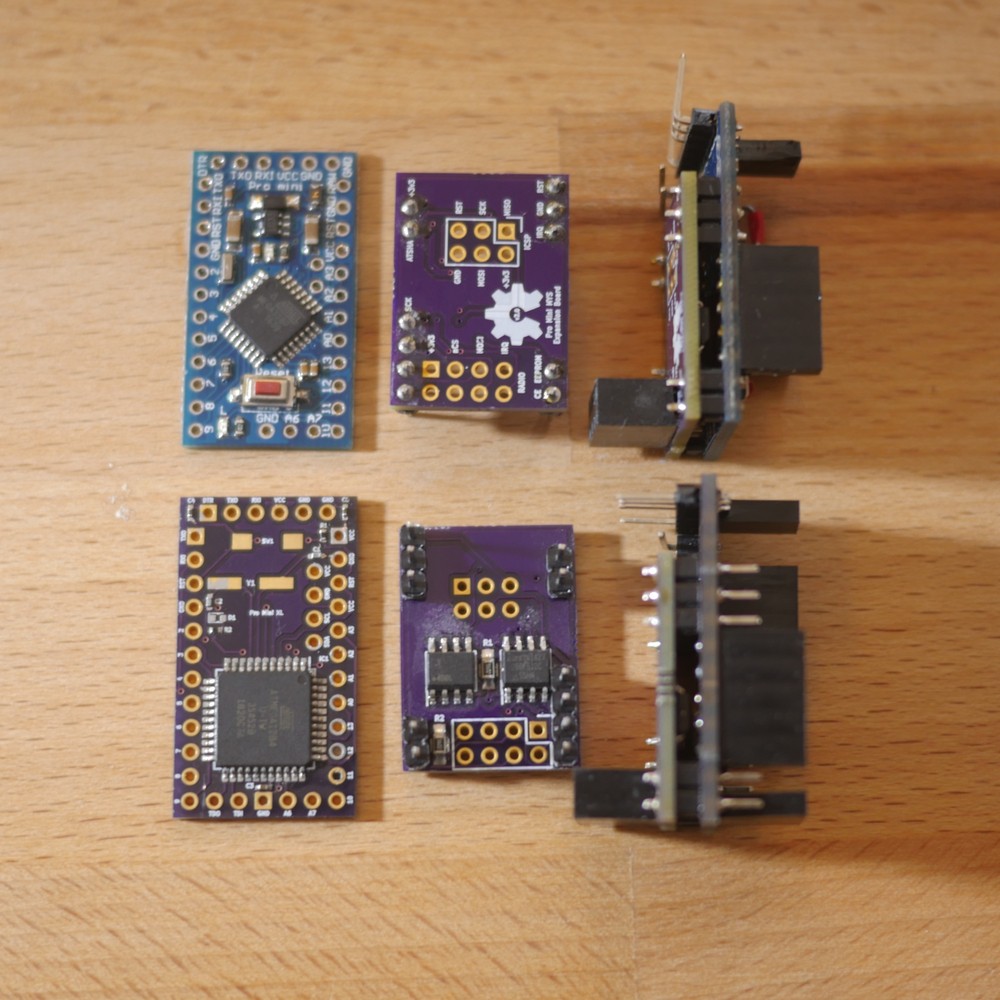
As a quick test, I plugged a freshly fabricated Pro Mini XL into an existing 328p Pro Mini daughterboard I’d made.
The board features a custom radio board socket, ICSP pins, ATSHA (for encryption) and external SPI flash (for FOTA updates).
![]()
I then added an RFM69HW and SI7021, the latter making use of the added power pins next to the I2C, and there I had a long-range wireless, temperature/humidity sensor with encryption and FOTA support.
![]()
However.
At this point, the 32-bit world was beckoning...
Over to you…
So that’s where I am with the Pro Mini XL right now.
- What do you think?
- What would you have done differently?
- What other components or features would you liked to have seen?
- How important is an on-chip regulator for your projects?
- How do you handle project power distribution?
Please let me know and I'll join you in the comments.
Thanks for reading!
- 4x the Program Memory
Searching for a better Pro Mini
I LOVE the Pro Mini! But it has limitations. To overcome some of them, I’m designing the Pro Mini XL & Pro Mini nRF52. What do you think?


 Nestor’s hardware modification is simply to power the mCard from the RPi 2’s 5v supply and interface.
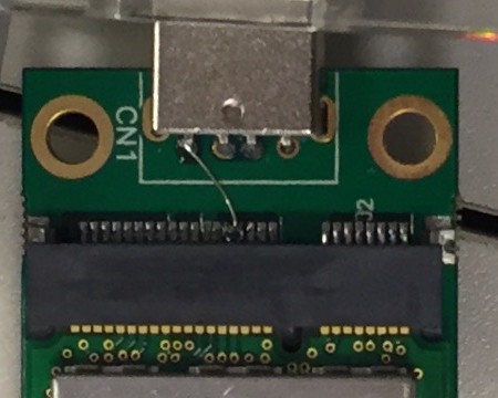
 Therefore, the new hardware is NO LONGER compatible with Nestor’s tutorial.
 Thermal Solutions
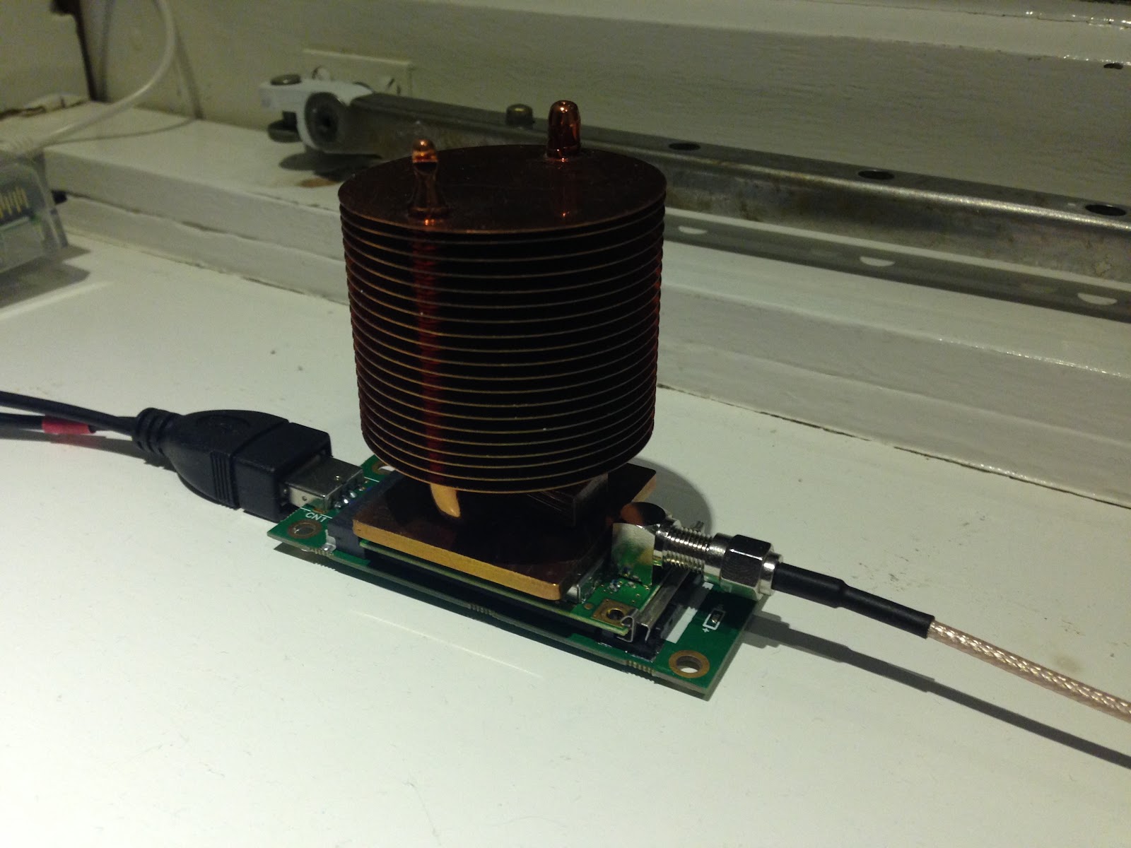 ...a very big heatsink!
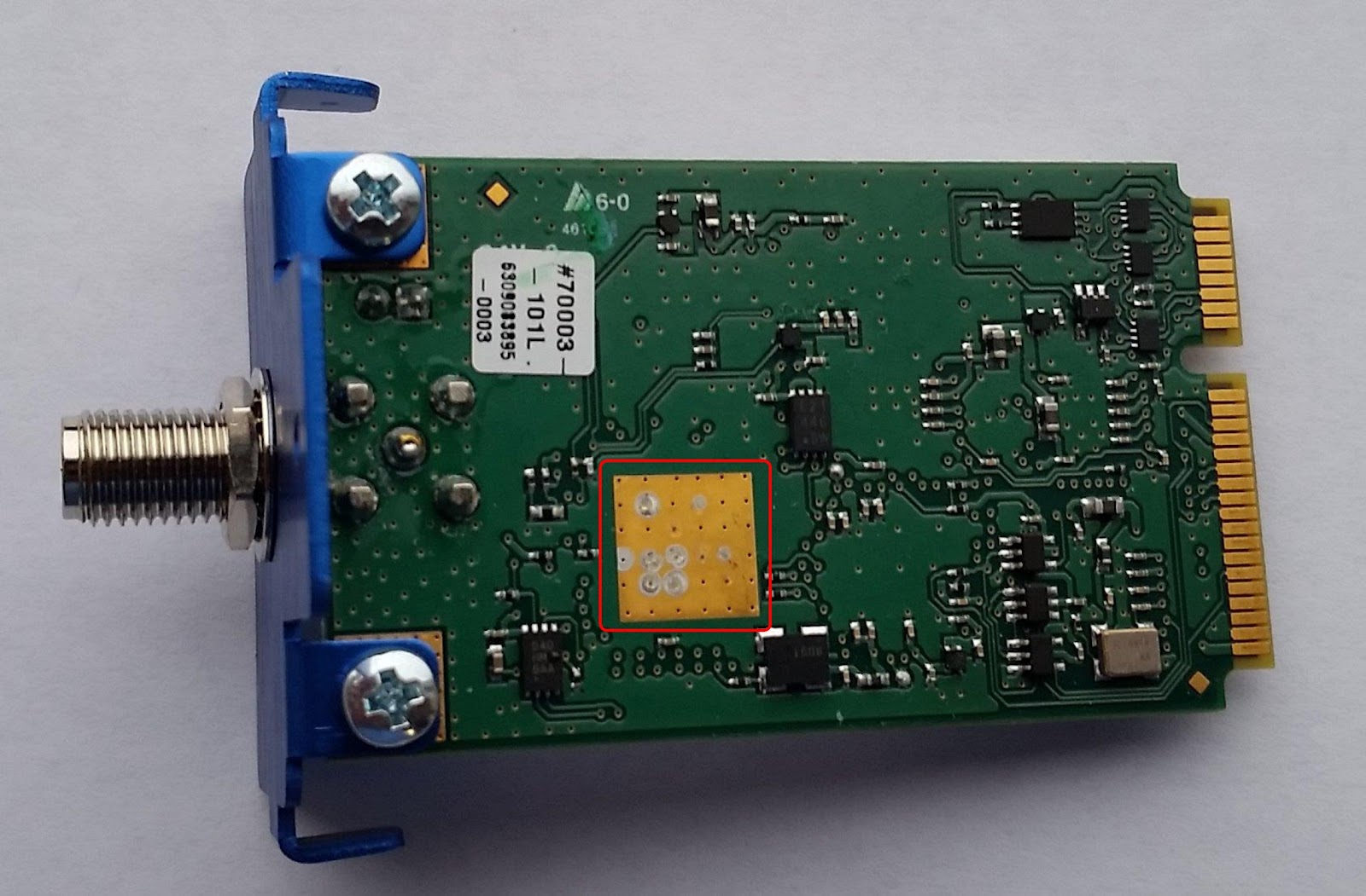 My gateways tended to become unpredictably unreliable (worst of both worlds) when they got too hot - and
 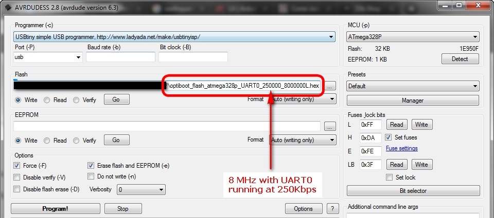 Why?
Why?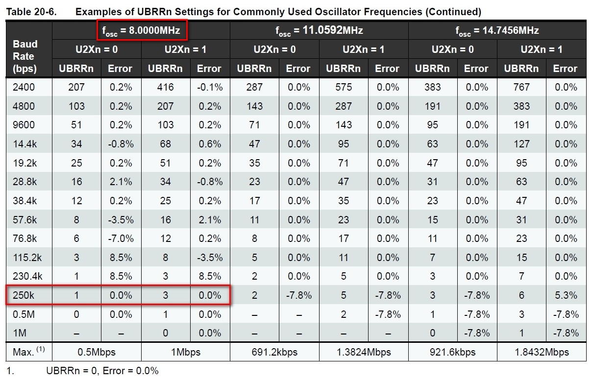 In fact, you’ll notice it’s still 0% right up to 1Mbps!
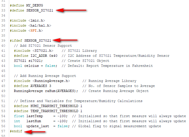 For the unfamiliar, wrapping code sections with #ifdef and #endif allows the compiler to ignore whole sections of your code if a #define is not present.
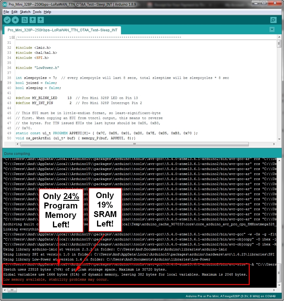 This (very) basic sketch uses up 76% of the available program memory and uses a further 81% of the available dynamic memory (SRAM).
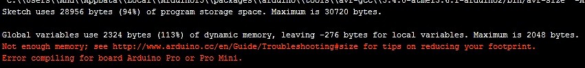

 Then I literally took the same wake-on-interrupt sketch and just changed the pin-mappings to those of the
 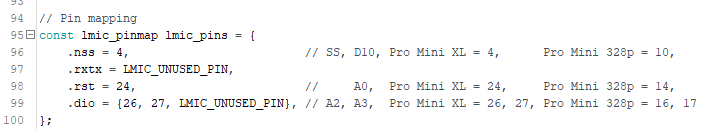 Finally, I needed to add the