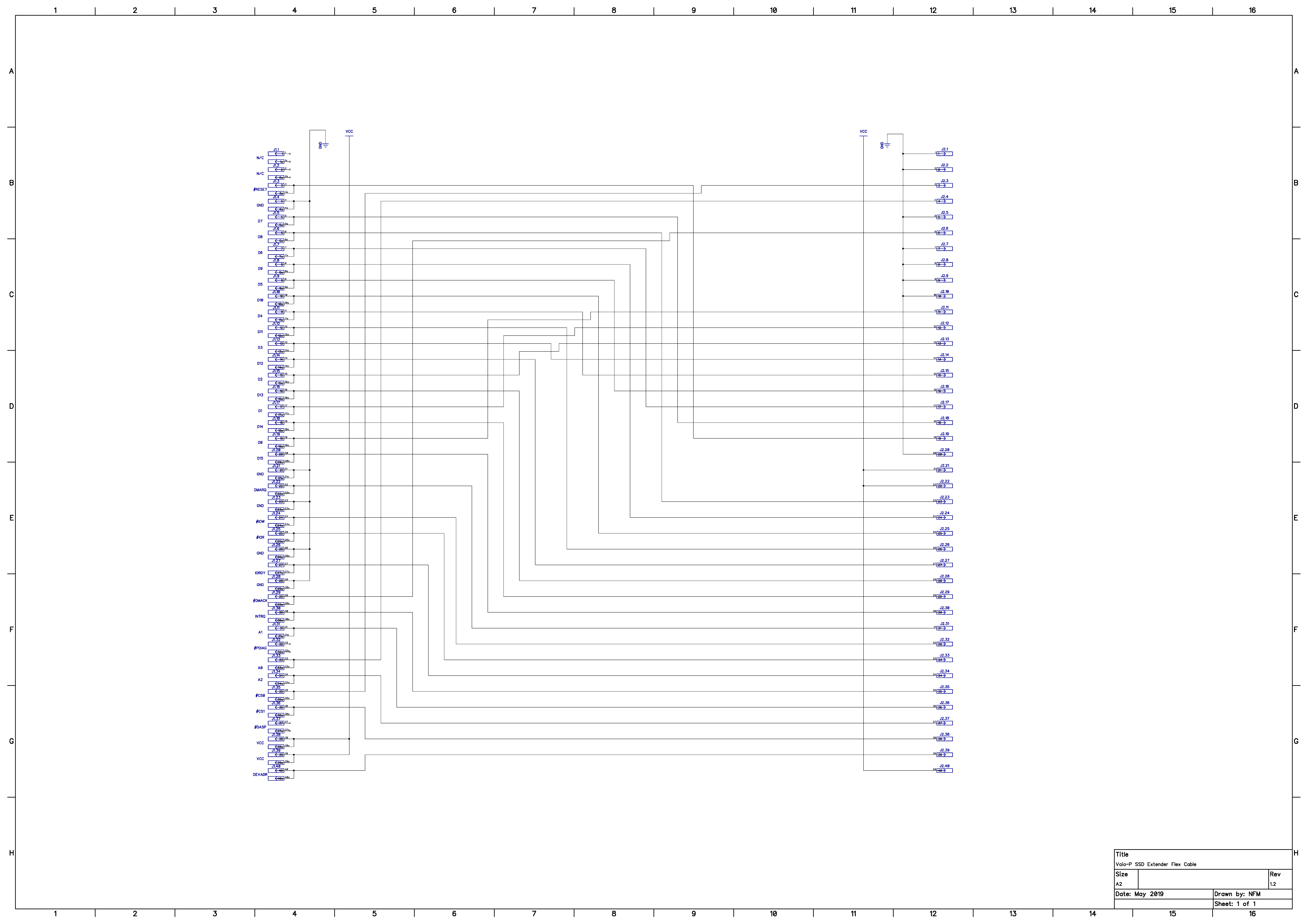
Here's the latest schematic. As dirty and messy as it is.....
Motherboard connector is on the right, ZIF pinout on the left.

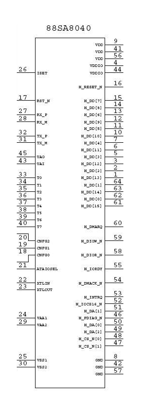
Pin 39 from the motherboard doesn't seem to have an equivalent pin in a HDD ZIF socket, it goes to pin labelled 'T1' (pin 34) on the Marvell 88SA8040 SATA Bridge chip.
I'm not sure what it does exactly (I think it's the 'device active' signal, to flash the HDD activity LED), so if anyone knows, let me know!
I have passed this pin through to pin 40 on the ZIF connector, it is used for Master/Slave select on the ZIF socket so it has no use here, so it will be fine to repurpose that pin.
It seems data is a bit hard to find on the Marvell 88SA8040 chip, beyond a basic pinout.
If anyone has more info, I'd be very grateful for anything that can be offered.

I've measured the voltage coming from the motherboard too, which is at 3.3V, so that's good. I only need one Vreg to give me a 1.8V rail.
Next step is to start designing the SSD daughter-board.
I think I'll forgo using the Marvell 88SA8040 chip due to it's lack of data etc, and instead use the more common JMicron JM20330.
The benefit is a data sheet and easier availability as it can be lifted from many ebay adapters.
 NFM
NFM
Discussions
Become a Hackaday.io Member
Create an account to leave a comment. Already have an account? Log In.