Bud Bennett
-
168 Hr Reference Aging Data
05/28/2019 at 21:21 • 0 commentsIt has been a week with the references running at the heater temp continuously. Here's the data (taken after the DVM ran for 1 hr at room temp):
2019-05-28 168hrs at temp
Meter params: HighZ, 100PLC, AZ on (Null for 1V and 100mV ranges)
Set Point: = 0.62785
Value Range
100.0068 100mV
1.000029 1V
2.49991 10V
4.99923 10V
10.00006 10VSo far so good. The 100mV reference drifted up by 1.1µV (0.0011%), tracking the upward movement of the 2.5V reference. The 5V and 1V references drifted up by 0.002%. The 10V reference did not move.
The box will remain powered for another 5 weeks or so.
-
Voltage Reference Results!
05/21/2019 at 19:15 • 1 commentAssembly:
I was careful to solder all of the surface mounted parts except the REF5025, which I hand soldered to the PCB using only the 5 pins that were connected to the circuit. I made sure to remove all of the flux with alcohol and a toothbrush. The through-hole parts were then hand soldered and the flux cleaned up as well. The LT1021 references were inserted into gold plated sockets. When power was applied all of the circuitry functioned as designed at first glance.
Two Problems:
I spent a couple of days chasing down bad assumptions.
The 2.5V Reference:
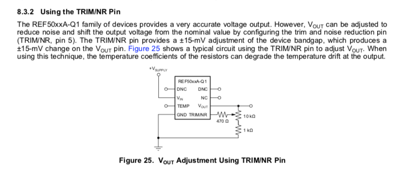
The TI REF5025 reference datasheet calls out the following circuit for the trim, which I copied without question:
![]()
When I first applied power to the board the two LTC1021 references measured within a few mV of the target value. The REF5025 was sitting at about 3.5V. My first thought was that I had a defective IC. I was able to trim the part in the range of 2.5V, but the trim was twitchy and even small tweaks to the trim pot generated several mV of change to the 2.5V output.
I Googled "REF5025 trim error" and the search brought forth many references to the data sheet -- even a data sheet with a Burr-Brown logo, which must have been published back in the last millennium. Nobody was complaining about the trim circuit.
I then removed the 470Ω ressitor from the circuit and measured the untrimmed output voltage -- which was within a couple mV of the correct value. I also measured the resistance of the TRIM/NR pid to GND with the circuit unpowered: 1MegΩ!
So now I'm thinking that there is some serious error in the data sheet and that the 470Ω resistor should be in the range of 470kΩ instead. So I soldered a 470kΩ resistor to replace the 470Ω and viola! (I used to play the viola) the trim became much more manageable. I could now trim the 2.5V output to less than a 50µV error.
The Heater:
The entire heater/reference system was supposed to be assembled into a small box with insulating foam to isolate the PCBs from the ambient temperature. When I tested the heater circuitry I used an open cell foam which probably does not have a very good R-factor. I used a styrofoam packing material when I assembled the two PCBs into the 100x68x50mm plastic box that I intended to use for this fixture.
The component values that worked for the bench testing did not work for the new box configuration. The improved insulation and enclosed box allowed for much lower power dissipation in the heater to reach the same temperature for the set point.
The first cycle with the breadboard component values required about two hours to settle to the set point temperature, but the step response indicated that the system was pretty stable with a phase margin of better than 45 degrees. But 2 hours is too long, so I replaced the resistor, R59, that was setting the integrator time constant with a smaller value, 100kΩ instead of 680kΩ, to decrease the overall time to settle. The result was a shorter settling time, but less phase margin (maybe less than 25 degrees). This is what the response to a perturbation looks like:
![]()
Pretty ringy-dingy, but it still settles to the correct set point in about 30 minutes. This data is produced by the Keysight 34461A DMM, which doesn't attach a timestamp to the data -- go figure -- I had to assume a sample rate for the above plot to get the time information for the x-axis. If this was a design meant to be for production I would never go for this, but for a one-off it might just work. It's pretty clear that my attempt to model the physical and electrical system was way off, but it's not worth the time to figure it out for just one instance.
OTJ Learning:
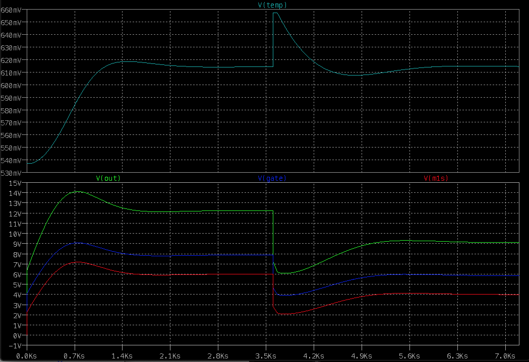
I trimmed the references to the target values, at room temperature (about 12°C in my shop), and then enclosed the heater/reference PCBs within the box. I let it settle for about 1 hour and took some measurements.
![]()
The high voltage references were spot on after trimming, but the 100mV reference was too high -- measuring 100.013mV -- 0.013%. I was expecting it to be less than 0.005%. In addition, the 1V reference was a bit high as well, measuring 1.00013V, which was above my target range. Both of these reference voltages were derived from resistor dividers.
I removed the top cover and proceeded to probe various nodes in the circuit to get an idea of what could be wrong. My initial suspicion was that there was a voltage drop caused by the PCB trace resistance. I measured a few voltages between various nodes across the PCB -- I found that there was about 50µV of offset due to thermocouple effects between one node or another with just a copper wire length and two solder joints between the two nodes. With that large of thermocouple error it seemed hopeless to expect the measurement error of a 100mV source to be less than ±10µV. But the thermocouple errors should cancel if the temperature differences are small. But then I learned that there was a "Null" button on the 34461A DMM. If you are measuring µV signals then the Null button is your friend.
Enlightenment:
While I was probing the PCB to try to determine what the problems might be I noticed that the temperature of the REF5025 IC was pretty close to the set point temperature. Apparently, the heater and reference PCBs are close enough that the heater can manage the temperature of the reference board even without a cover applied. The power requirements will be higher, but it was doable.
So I just trimmed the references (with the Null feature subtracting the µV errror, as if they were in the box and regulated to the set point temperature. After I closed the box and screwed the lid down I let it soak for about 30 minutes. And then took the following readings (DMM settings: 100PLC, AZ on, High Z):
100.0057mV (0.0057% error) (nulled) 100mV range
1.000005V (0.0005% error) 1V range
2.49989V (-0.0044% error) 10V range
4.99913V (0.0174% error) 10V range (trimmed to produce accurate 1V reference)
10.0006V (0.006% error) 10 V range
These readings are well within the specification tolerances of the 34461A DMM. I'm going to let it run for about 1000 hrs (~6 weeks) and see what kind of aging drift shows up.
-
Results!
05/15/2019 at 23:22 • 0 commentsThe Keysight 34461A arrived today! I completed the current reference board yesterday...almost perfect timing. I plugged in the 34461A and let it warm up for a couple of hours at room temp (72°F/22.2°C). I adjusted the current reference potentiometer to put the three current reading errors approximately centered between the three readings. I took these photos of the front panel for each of the three current reference values, with Aperture set to 100 60Hz line cycles, and Auto Zero on.
![]()
![]()
![]()
I received a calibration certificate with the unit. Here's the relevant data:
DCI 10mA on 10mA range. Reading: 0.0100000 Error: -0.0003%.
I don't know what these guys are smoking, but the above line of text doesn't make any sense. I believe that if they are truly reading 10mA on the 10mA range then the reading should be 9.99997. It seems that they have the DMM range set to 1A, which would yield the correct reading of 0.01 for a 10mA current. They did not calibrate for lower values than 10mA! Let's assume that the 34461A is perfectly accurate and go from there.
The first reading on the 100µA range has an error of +0.0018% (90 day spec = ±0.065%), that's 1.8nA. The second reading on the 1mA range has an error of -0.0028% (90 day spec = 0.036%. And the third reading on the 10mA range has an error of -0.0052% (90 day spec = 0.032%).
So it appears that the current reference accuracy is at least 6x better than the tolerance of the 34461A. Not bad!
[Edit 2019-05-21]:
I found a major flaw in the layout when I proceeded to take a 10mA measurement with my old HP972A DMM. The ground lead of the 1000µF filter capacitor is dangerously close to the common probe pin. The probe slipped off the lead and shorted the meter across the 15V supply. That blew the protection fuse and killed the BAV70 diode clamp on the 10mA output. That was the first time that I'd ever blow a fuse on a meter...since the 1960's!
I desoldered the filter cap and installed insulating sleeves over both leads before reattaching it.
The other problem that I noticed is that the HP972A measures the 1mA source inaccurately -- about 20% low on the 4000µA range, but gets the correct value (0nly two digits: 0.99mA) on the 40mA range. It turns out that the meter uses a 550Ω shunt resistor to measure the current on the 400µA and 4000µA ranges, and an 8Ω resistor to measure current on the 40mA and 400mA ranges. The 550Ω resistor develops 0.55V across it when measuring 1mA -- this is enough to turn on the BAV70 diode and siphon off some current to the supply. The solution is to put a small battery in series with the DMM to boost the voltage above the supply. A 1.5V cell should do the trick.
If I was going to redesign the circuit I would add another BAV70 diode between the anodes of the three clamp diodes and the positive supply rail. That would provide a compliance of nearly 1V.
-
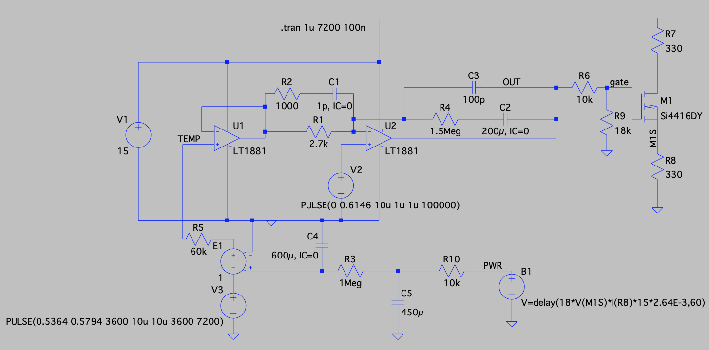
Experimenting With The Heater PID Controller
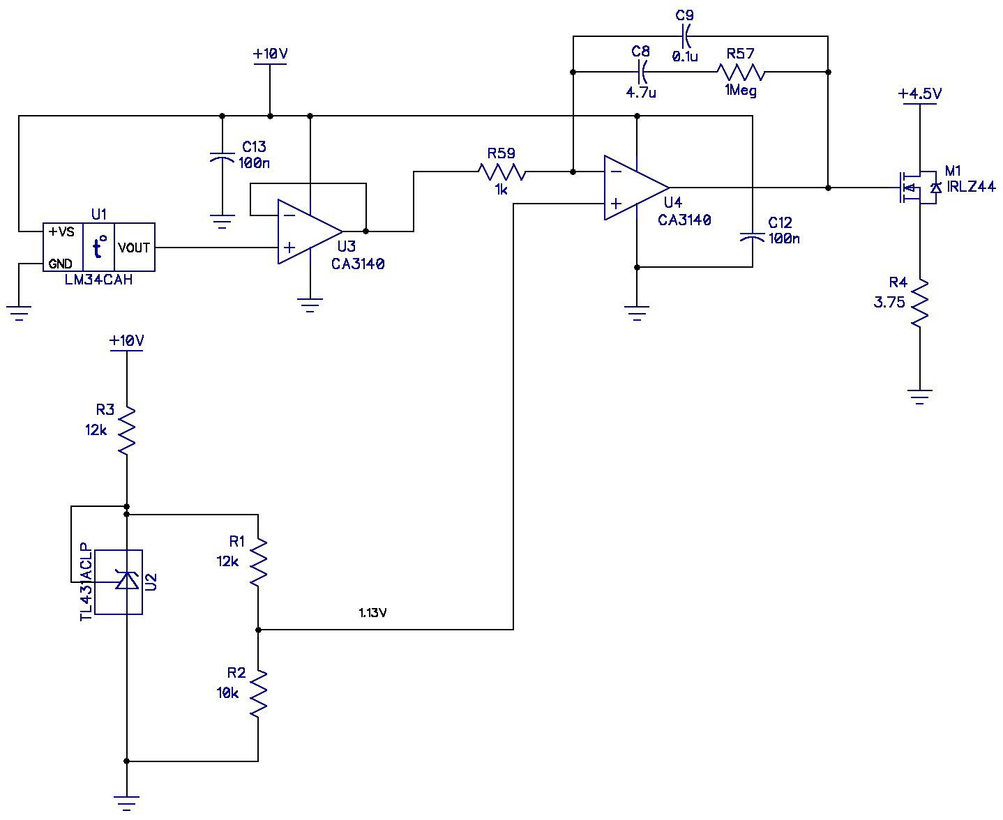
05/03/2019 at 00:01 • 2 commentsBefore I committed to fabricating the PCBs for the voltage reference I decided to conduct a simple experiment to get a handle on possible problems controlling the temperature of the enclosure. I chose two CA3140 opamps from my inventory (probably 40 years old) for the two opamps. I also found some LM34 temperature sensors in metal cans that probably hailed from the 1970s. A IRLZ44 FET completed the component search and I integrated them all into the following schematic.
![]()
The LM34 was taped to the middle of the array of resistors that made up R4. U2 provides a 1.13V reference for the LM34, which should cause the PID to regulate the temperature of R4 at about 113°F.
The 4.5V drain voltage on M1 in combination with R4 should generate 5.4W of power across R4 to lessen the amount of time required for the heater to reach temperature.
I wired the LM34 with 8 inches of lead wire and taped it to the center of the PCB containing the R4 resistors. I then wrapped the enclosure with Duck tape to seal the edges of the foam enclosure around the R4 PCB.
I flipped the switch on the two power supplies and watched the show. It was pretty boring. The temperature of R4 slowly ramped from 56°F to about 115°F in about 15 minutes. When my temperature probe indicated 120°F the gate of M1 started to drop to about 5.6V and the PID took over the temperature regulation of R4.
For the next 15 minutes I watched the display of the temperature probe. It varied from about 119.6°F to 120°F. That's only 0.22°C. I observed no anomalous behavior or strange oscillation of either the gate voltage of M1 or the temperature reading of the probe.
It appears that the PID controller is ready for prime time.
[Edit 2019-05-12]:
Later in the day I attempted the same experiment with the PID temperature controller. The shop temperature had increased to around 60°F by then. When I applied power to the bread board it oscillated rail-to-rail -- not what I expected. I determined that the cause for the stable response was that the Z44 FET was in its triode region and the system gain was relatively low. When the ambient temperature increased, the FET came out of its triode (linear) region, which increased the open-loop gain.
I also found that the opamp U4 was oscillating because of the load capacitance -- the drain-gate capacitance of the FET. This was fixed with a resistor divider 10K on top, 12k on bottom, between the opamp output and the FET gate. Unfortunately, the system now oscillated rail-to-rail with a 5 minute period. After 2 days of fiddling with the breadboard I determined that the problem was a 60 second delay in the heater. A delay is really bad news since it is an exponential phase error. A 60 second delay is totally awful. I was unable to get a stable system by substituting components and waiting 20 minutes for the system to settle into a steady-state bang-bang oscillation.
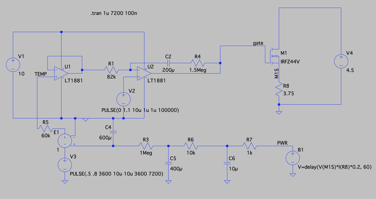
Now I turned to LTSpice to simulate the problem. LTSpice will yield a reasonably accurate result (if your models are accurate) in a few seconds instead of waiting 15 minutes on the bench. Here's what I eventually came up with as a working model:
![]()
The heater is modeled with a behavioral voltage source, B1, that converts power to voltage to emulate what the LM34 is doing. B1 also inlcudes the 60-second delay in the heater. The RC network tries to model the time constants involved with converting power to temperature. Heat transfer is a linear differential equation which can be modeled as a simple RC time constant between each physical interface. Note that C2 is now 200µF, a considerable increase from the initial 4.7µF. V3 simulates a changing ambient temperature from 50°F to 80°F to get a feel for how the loop gain affects stability as the ambient temperature changes. This circuit accurately modeled what I was seeing on the bench with the original component values -- a rail-to-rail oscillation with a period of several minutes.
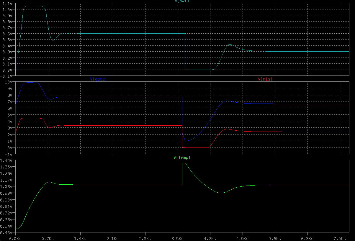
![]()
The above is a two hour simulation. Note that the system settles in about 1/2 hour and the overshoot and ringing are consistent with a 50° phase margin for the 50°F ambient case, and overdamped when ambient is 80°F.
I plugged similar component values into the breadboard and lo and behold the system settled to a stable value at 110°F. I then changed the setpoint to 85°F and when I came back after an hour the system was holding that temperature. (Ambient was 60°F in both cases.)
Changes to the PCB components:
I modeled the heater system on the PCB with the circuit below.
![]()
B1 emulates the temperature sensor in the REF5025 voltage reference IC, with the included 60 second delay. Since the PCB has been ordered I have little leeway with component sizes. In particular C2 will be a stack of 2 100µF 1206 capacitors in place of the original 0805 capacitor. The simulation results are similar to the breadboard simulated results.
![]()
Again, the system settles to within a fraction of a °F within about 1/2 hour after turn on. I haven't yet assembled the heater PCBs and installed them in the plastic box. Things may change. I'll edit this log if things don't work out as planned.
[Edit: 2019-05-14]:
Well...I wasn't thinking clearly when I posted the previous edit. I am having trouble finding a 200µF ceramic capacitor (or even two 100µF) with more than 15V rating. So the simple fix is to increase the resistor values by a factor of ten and reduce the capacitor from 200µF to 22µF. It did not quite work out that way in the simulations, but I'll wait until I can assemble a heater board and test it on the bench, and in the box, before publishing any more changes.
The TLV170 opamps have an input bias current of 10pA so the increased resistance won't significantly affect the temperature setpoint error. I don't normally use any resistor value above 1MegΩ, but this circuit will be enclosed in a nice case and I will make sure to clean off any solder flux residue.
-
A Current Reference Too
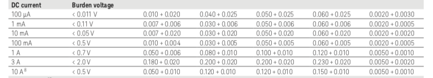
05/01/2019 at 23:00 • 0 commentsIt was inevitable. Checking voltage accuracy is all well and good, but not enough. I have been thinking about how to provide a set of reference currents that are accurate enough to keep the 34461A honest for a few years. It's tough, but doable. The 34461A specs for DC current are:
![]()
I tried to design for four reference currents, but gave up on the 100mA current -- too much power dissipation (1W) with the approach that I chose. So the current reference will provide only three currents: 10mA, 1mA and 100µA. In much of my work the accuracy of currents exceeding 10mA is usually not critical. The circuit below is what I came up with after a few revisions.
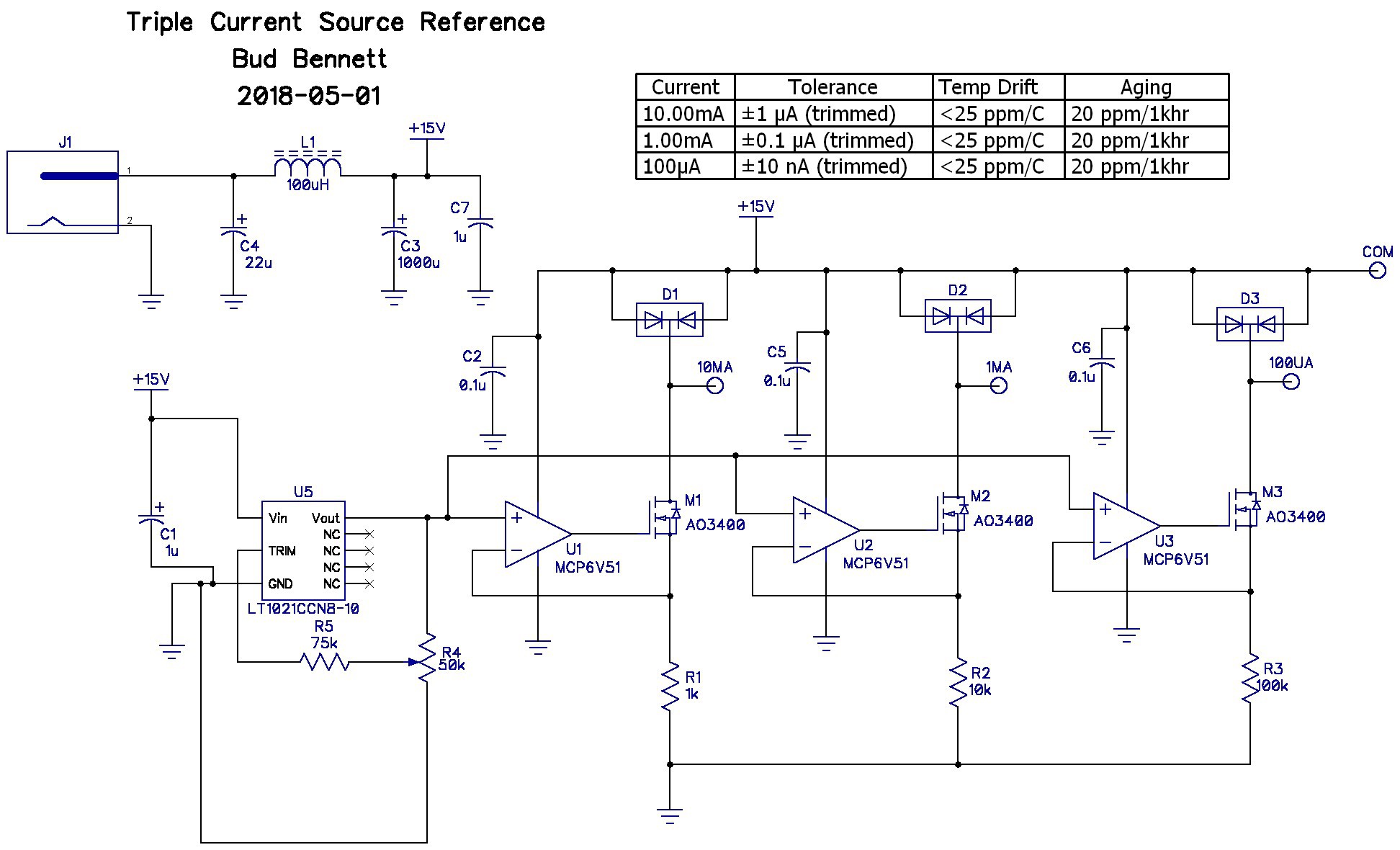
![]()
Current is just V/R. You need a good V and some good R's. This is a lot different that making an accurate voltage reference where ratios of resistors are important. In this case the absolute value of the voltage reference and the resistances determine the accuracy of the current. I chose the LT1021C-10 for the voltage reference. It has an initial accuracy of 10V±5mV. I added a trim to improve it, hoping to get 0.1mV trimmed accuracy.
I entertained the thought of just having the DMM measure the current through the resistor directly, but the burden voltage is too high and injects an unspecified error into the measurement. In the circuit above the DMM will connect between the COM pin and the current source to be measured — there is no need for large voltage swings. This makes the design a lot easier than a general purpose current source. Note that when the a current source is not being measured its current flows into a diode to limit the voltage swing to less than 1V below the supply rail, keeping the opamp and FET operating normally. When the DMM is measuring the current source the voltage across the diode will only be a few mV and the diode will have a negligible effect on the measurement.
The resistors, R1-R3, are expensive, 0.01% initial tolerance, 10ppm/°C tempco, through-hole types (~$7/each from Digikey). If the opamp has low offset and drift then the current in the drain of the FET transistors, M1-M3, should be very close to V/R. I chose the MCP6V51 chopper stabilized amplifiers for this reasoning: low Vos (15µV max), low Vos drift (36nV°C), very low input bias current (80pA), single supply operation to 45V, with moderate GBW, low supply current (470µA), in a small SOT23-5 package.
With a reference trimmed to 0.001% and resistors specified to 0.01% I expect the current sources to be on the order of 0.01%, if I don't screw up the PCB layout. This assumes that there is no significant leakage from gate-to-source or gate-to-drain from the AO3400 FET ( I checked -- the data sheet says < 100nA @ 12V VGS), so I'm hoping that there is less than 1nA of gate leakage current with room temperature conditions and lower gate-source voltage.
There are a lot of things to worry about with the PCB layout -- is the reference voltage compromised by load currents through traces?, or is the trace resistance low enough to not degrade the tolerance of the expensive resistors? Or are there parasitic leakage currents from nearby traces?
I added guard rings around the sensitive nodes -- the probe points used for the currents, and the high-voltage terminals of the R1-R3 resistors. Elsewhere I made sure that the PCB trace resistance was negligible where it made a difference (the GND terminations of R1-R3). The GND pin of the LT1021 connects to the GND trace of R1-R3 with little current flowing in the trace, so voltage error should be minimized. Also, the connections of the opamp and the source of the FET are Kelvin to the top pin of the resistor.
If the PCB parasitics are eliminated (or at least minimized) then all that’s left is the errors from the voltage sources (the Vref and opamps). The 80 pA input bias current of the opamp, and the value of the resistor. I expect the Vref to be trimmed to around ±0.1mV (±0.001%). The opamps contribute 15µV, or 1.5ppm, which is only 0.00015%. The resistors will dominate the error, so assume that the initial error will be very close to 0.01%. That’s about 5x better than the specification of the 34461A, but we haven’t accounted for temperature or aging errors.
Temperature drift of the reference is specified as <20ppm/C over its temperature range. The typical drift is quite a bit lower — 5ppm/C — and even lower over the small range of expected temperatures the circuit will be exposed to in the lab. The opamp is chopper stabilized with nearly zero offset voltage drift (36nV/C). That leaves the resistor with 10ppm/C. Over the ±8.5°C range of operation the current sources should move less than ±0.013%.
While the aging characteristics of the voltage reference are known within bounds, and the opamp errors are insignificant, the resistor aging is largely unknown. I saw references to ±0.01% drift after 2000hrs @70°C, or ±0.03% after 8000hrs at rated temperature and power dissipation, and a stability of X ppm after one year of shelf life. I guess we’ll see what happens. I don’t plan on running the current reference for months (or even hours) at a time to let it burn in.
I’m ready to order PCBs tomorrow.
-
Adding A 1V Reference Voltage
04/29/2019 at 21:44 • 0 commentsI’ve been bothered about the choices for reference voltages lately. My new Keysight 34461A has voltage ranges of 0.1V, 1V, and 10V. My old HP972A (a freebie) has ranges of 40mV, 400mV, 4V, 40V, etc. If there is not another reference around 1.0V the 34461A I will not be able to test that range effectively. The 972A can use the 0.1V, 2.5V, and 10V references to cover most of its ranges. It’s interesting that neither the HP or Keysight DMMs need the 5V reference for calibration.
The easiest way to get 1V is to divide it down from another reference voltage. I chose to make a 1:5 divider from 5V to get the 1V reference. The divider uses the same 20kΩ resistors that went into the 0.1V reference. It will not use 50 resistors (there’s no room on the PCB) and will require the loading of the DMM to be higher than 10MegΩ — therefore only useful to the 34461A.
The accuracy of the divider is expected to be only around 0.05% (0.1%/√5). But the 5V reference can be trimmed to yield the correct value at the 1V output if the 5V output is not expected to be used as a voltage reference for calibration. That’s the plan.
Either the 5V or 1V references can be brought out to terminals with the current PCB layout, but I expect to not use the 5V option, given the ranges of my current collection of DMMs.
Both the layout and schematic have been updated in the project details section to reflect this change.
-
The Heater
04/26/2019 at 22:52 • 0 commentsI need the heater to keep the reference PCB at a constant temperature while the ambient temperature varies from about 10°C to 30°C. The heater PCB will be about the same dimensions as the reference PCB in order to fit into the case. I expect to insulate the two boards with about 1/2" of open cell foam, with a thin piece of foam separating the two boards within the enclosure.
To wit, I set about to determine how much power the heater would require to keep the temperature at the desired value. There is a lot of fat finger estimation going on here, but you gotta start somewhere. If I get it wrong it's not the end of the world.
I found that the amount of power needed to drive the system to 30°C from about 18°C is surprisingly small -- only about 2W, depending upon the degree of insulation within the box.
The Experiment:
I have a couple of PCBs that are populated with an array of 10Ω/1W carbon resistors that were created explicitly to be a heater. I enclosed one of these PCBs in a sandwich of open cell foam with a thickness of about 1/2 inch. I made a good effort to seal the edges to prevent air movement and leakage. I also placed a K-type thermocouple lead in the middle of the PCB to take the necessary temperature readings.
The experiment consisted of applying a known power dissipation across the PCB and measuring the temperature rise from ambient temperature after the internal temperature was allowed to stabilize. The purpose of the experiment was to estimate how much power would be necessary to keep the temperature internal to the enclosure constant over the expected external ambient temperature range.
The Results:
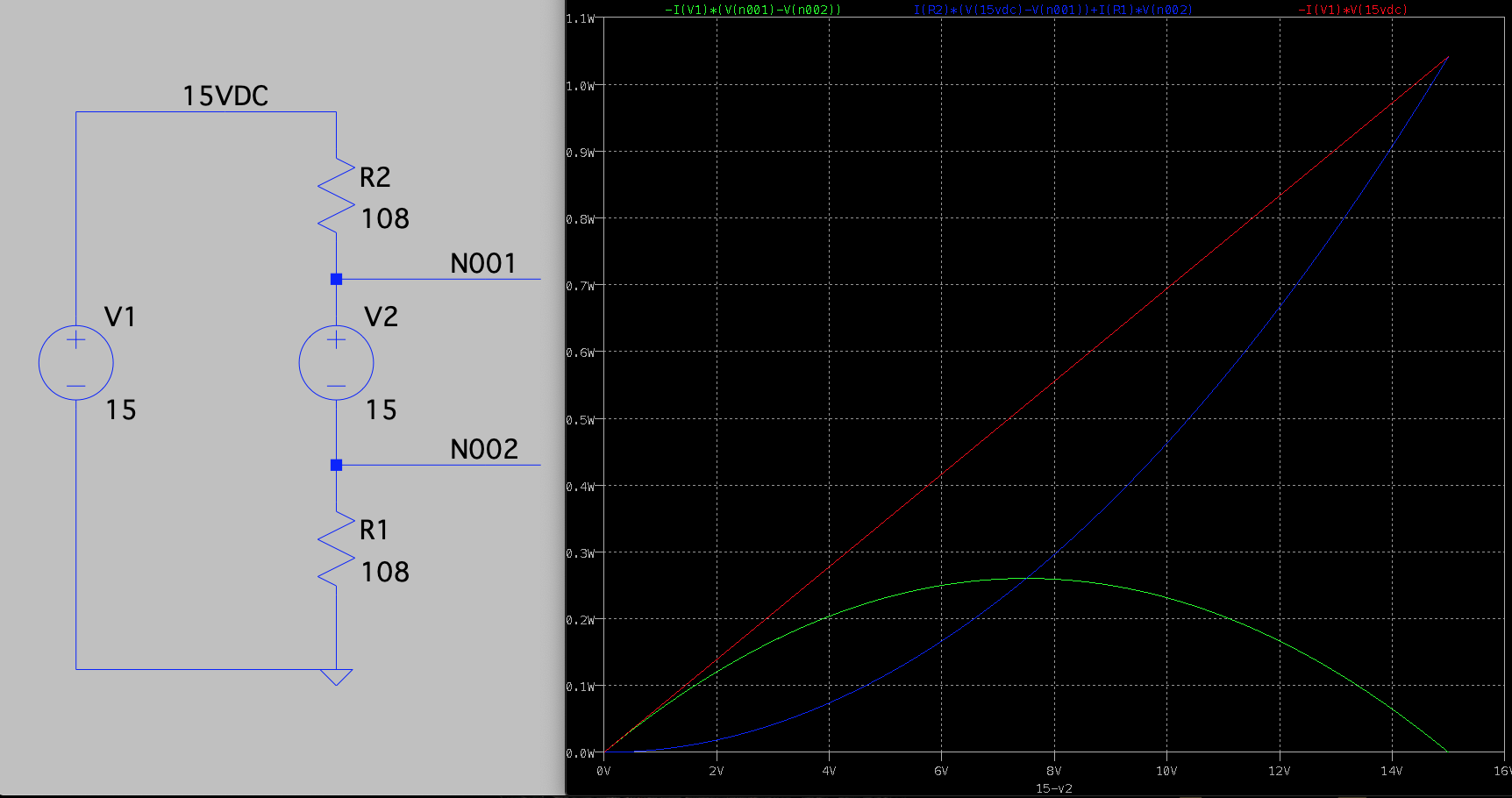
I applied exactly 1.0W of power to the resistor array and waited until the temperature stabilized -- about 1 hour. The difference between the internal temperature and the ambient temperature was 11°C. I then applied 2W of power and got a 22°C rise. I measured a 33°C rise with 3W applied. This translates to a thermal resistance of 11°C/W.
I also ran a simulation of the proposed heater circuit to see how the power dissipation varied between the active devices and the passive devices. The green trace is the power dissipation in the FET (or voltage source in the simulation), the blue trace is the power dissipation across the resistors, and the red trace is the total power dissipation in the circuit. It turns out (no surprise) that the preferred power dissipation should be between Pmax and Pmax/2 so that the passive devices dissipate most of the energy instead of the active device. Here's a plot of the relative power dissipation between the FET and the resistors. I was assuming that the heater would require 10W maximum which was too high by a factor of three.
![]()
But it is interesting to note that the maximum power dissipation of the active device peaks when there is 1/2 the supply voltage across it.
The Design:
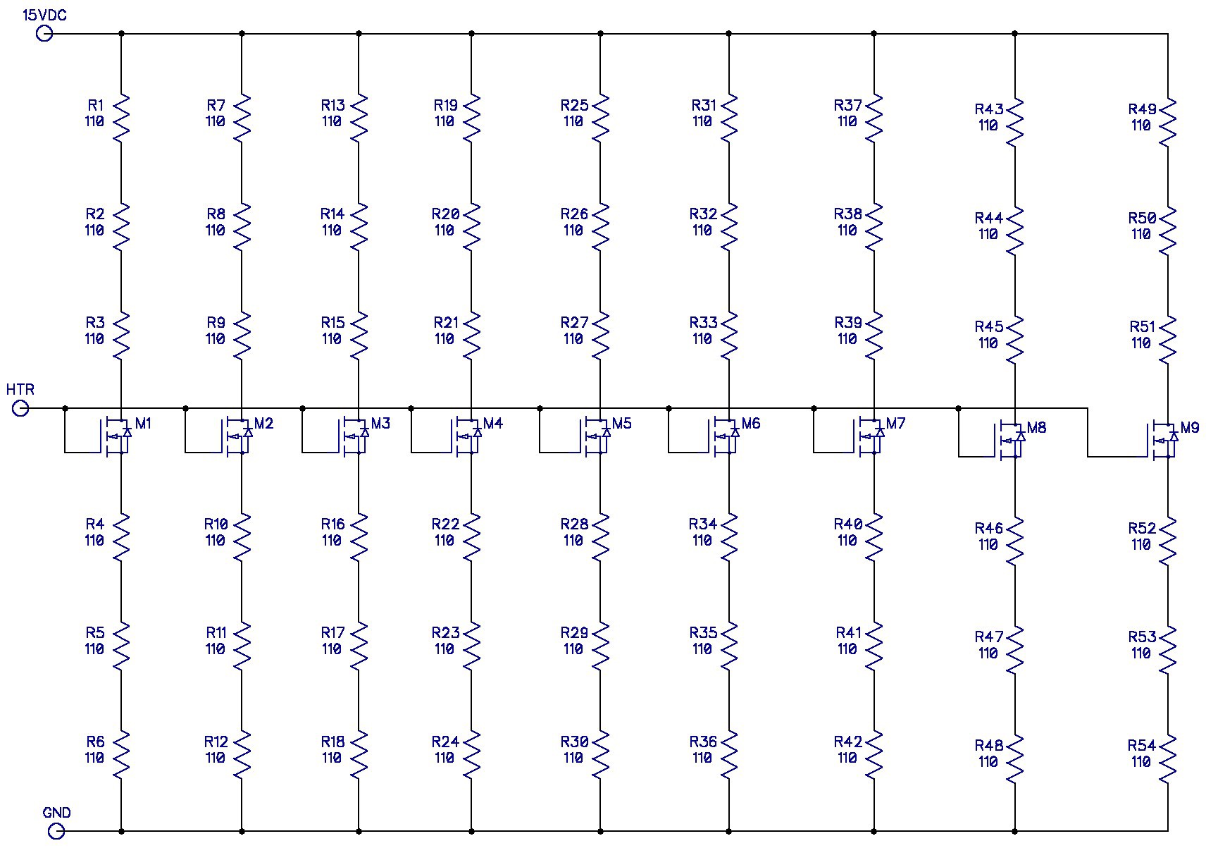
This is the first pass of the design for the heater:
![]()
When there is nearly zero volts across the AO3400 FETs the maximum power dissipation is a bit over 3W: 9 x 15V^2/(6 x 110Ω). In that case the power will be dissipated across all of the resistors and very little power consumed by the FETs.
The smallest estimated power dissipation is about 1W, when the ambient temperature is 80°F (27°C) and the circuit is attempting to keep its target temperature at 100°F (38°C). In this case most of the power is dissipated across the FETs, but it is not a significant amount and the expected temperature rise is only about 6-8°C in the FETs. I estimate this based upon the AO3400 data sheet which claims that the thermal resistance from junction to ambient is between 80-100°C/W.
The resistors are 2512 smd 5% tolerance. They are rated at 1W maximum dissipation/each, with an expected thermal resistance of 80°C/W.
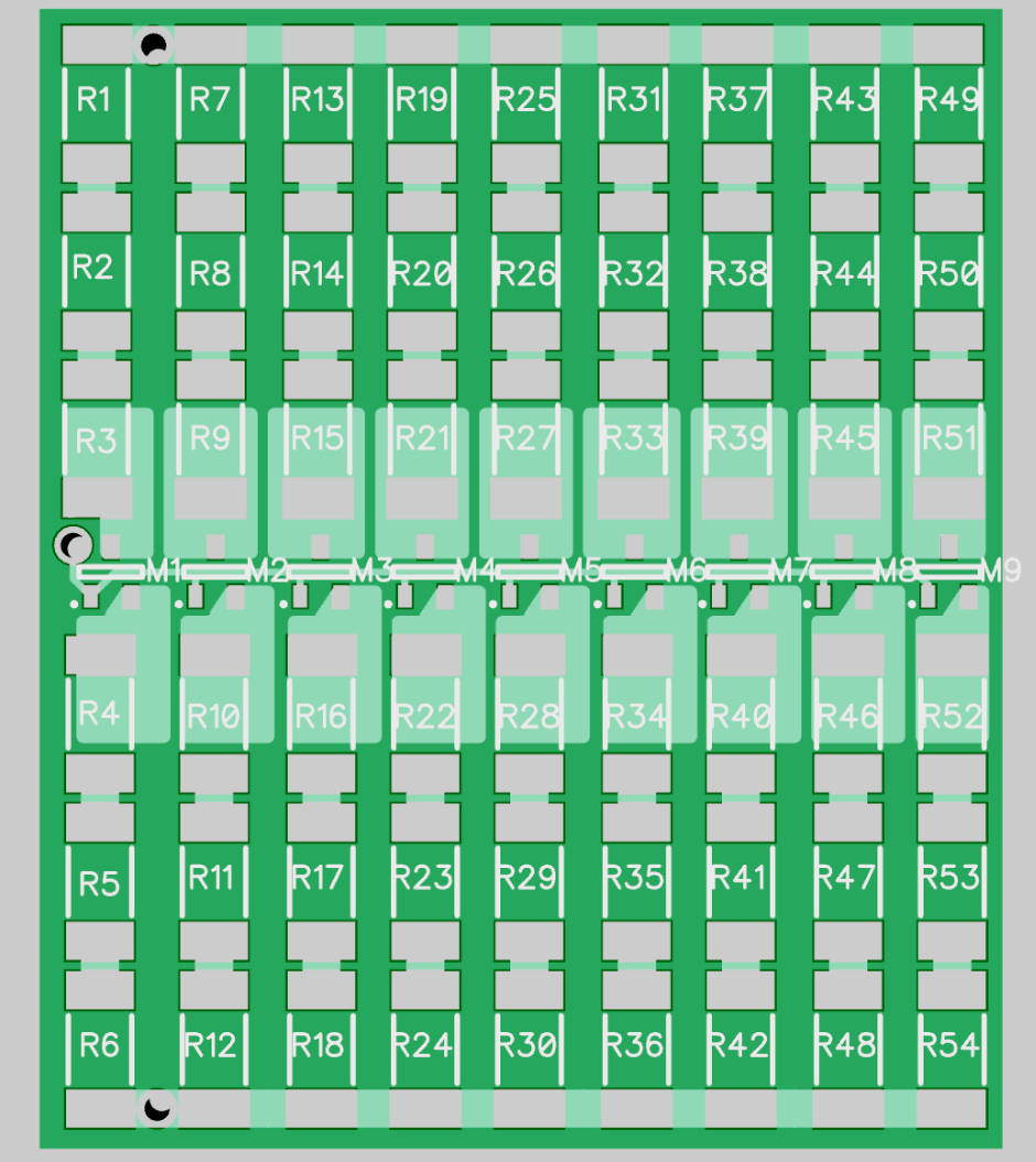
If I get it wrong, then it is a simple matter to order resistors with a difference value to populate another Heater PCB. Here's what the PCB layout looks like today:
![]()
I placed a lot of metal around the FETs to distribute their heat across the PCB. There is also a large ground plane on the back side (which will face the refrerence PCB) to help even out temperature differences even further. The PCB is the same size as the reference PCB to make the packaging easier.
-
The Input Filter
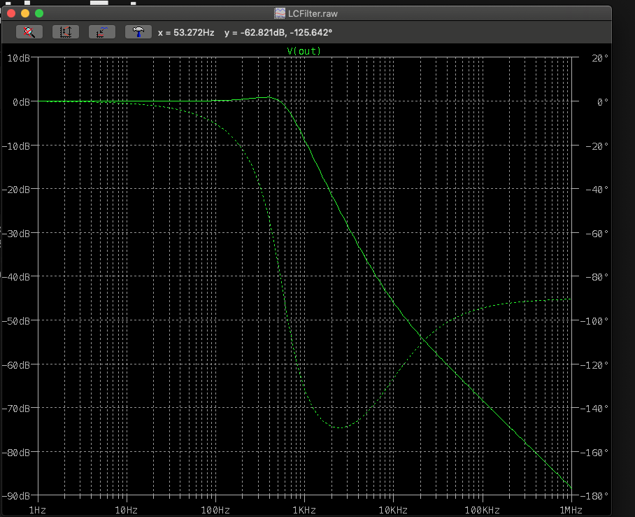
04/25/2019 at 21:10 • 0 commentsI decided not to employ a separate linear regulator to power the circuit. I did not want the additional source of heat or the possible temperature gradient. Therefore I'll just use a 15V wall adapter as the supply for the entire system. The wall adapter is a switching power supply so I must get rid of the switching noise. I tried several combinations of inductor/capacitor filters and settled upon a 100µH power inductor followed by a 1000µF/25V electrolytic capacitor. A big factor was that I have both of them already in my inventory.
The LTspice AC simulation predicts the typical 20kHz switching noise to be reduced by about 55dB.
![]()
-
Resistor Divider Layout
04/25/2019 at 19:01 • 0 commentsObtaining an exact 25:1 ratio is a difficult task. I wanted to keep the output resistance of the divider relatively low to help minimize any loading effects. A 20kΩ divider resistance with a 10MegΩ load from a volt meter will cause a 0.2% (200µV) error in the measurement. The 833Ω divider resistance yields a more reasonable 8µV error.
But the metal interconnect resistance between 24 parallel 20kΩ resistors causes significant errors. 1 oz. copper PCB traces have a sheet resistance of about 0.5 mΩ/square, with a tempco of 3900ppm/°C. The large tempco will destroy any accuracy the divider has if the trace resistances connecting the divider to the input source don't match correctly. This means that PCB trace resistances must be calculated as part of the divider ratio.
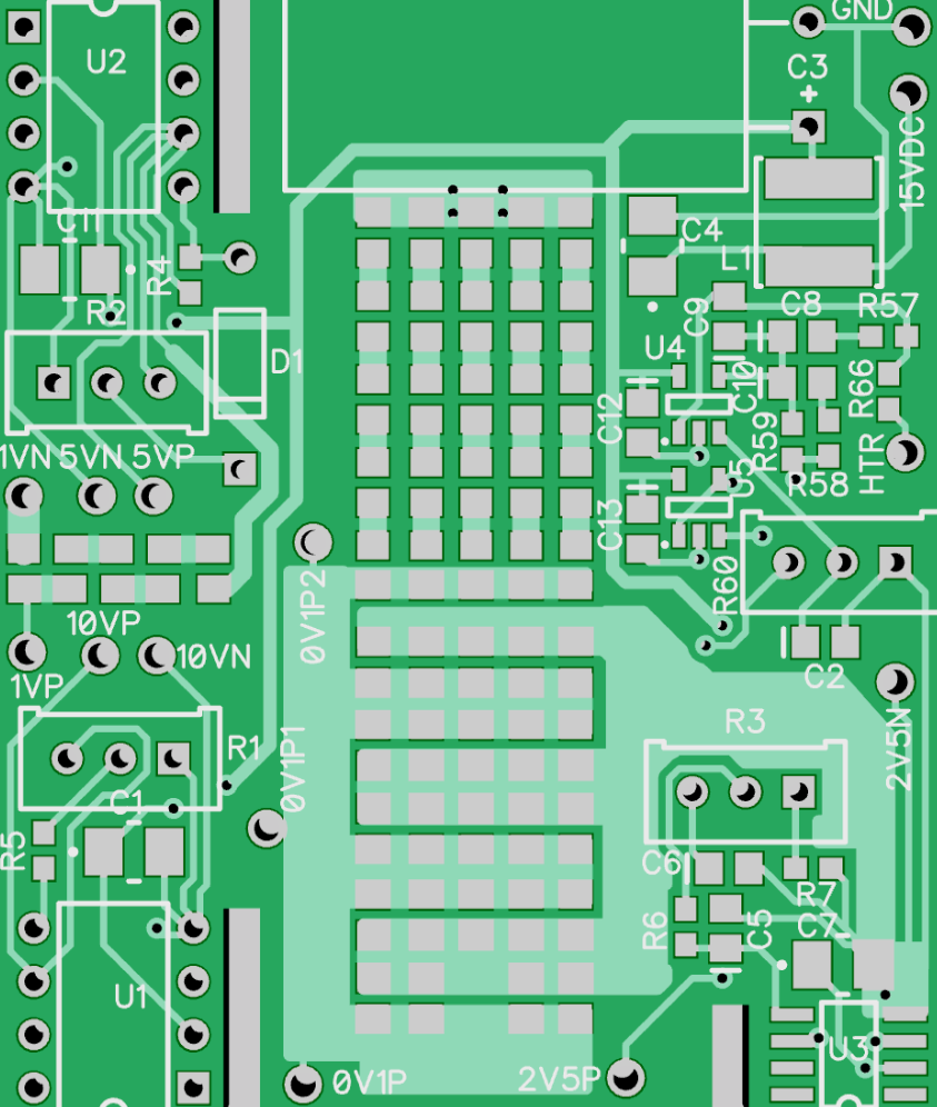
My first attempt to layout the resistors resulted in too much distance between the resistors -- I had to remove the reference designators from the top silk screen in order to pack the resistors more closely. My best effort to date yields about 7 squares of copper trace from the 2V5N kelvin connection at the GND pin of the REF5025 IC. That's only 3.5mΩ of resistance -- I was pretty proud of myself until I calculated the static error and temperature effect on the ratio and got 10µV of error with a 17°C change. Here's the top of the PCB layout:
![]()
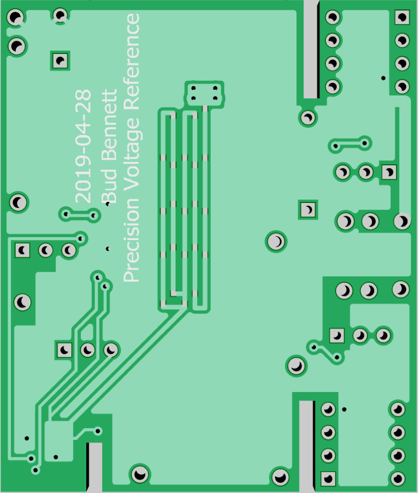
It turns out that the ratio of the PCB trace resistances must match the resistor divider ratio in order to cancel out the errors of the traces. I needed to get 7x24 = 168 squares of trace resistance to the top of the divider. That's more difficult than it first appears. The trace width needs to be less than 10 mils to obtain 168 squares of metal from the top of the divider to the VOUT pin on the REF5025. The variation of a 10mil trace is not something I want to depend upon. The approach that I took was to use a serpentine route using a 20 mil wide trace. There should be much less width variation on a 20mil trace than a 10mil trace.
![]()
My rough calculations now show a +0.17µV error at room temperature, which expands to +3µV with a change of 17°C. If I choose to use 2 oz copper, then the error drops to +1.5µV over temp. Still paranoid that I missed something, I added pad openings along the trace so that I could measure the error and possibly short out some of the trace to correct some of the error. If the trace needs to be longer, then I can cut the shorted trace on the left and short between pads to get the desired result.
In addition, I added three pads for different pick off points along the length of the parallel resistors. If there is a measurable difference between the three points then just pick the best one to feed to the terminal.
-
Lies, Damn Lies, and Statistics
04/23/2019 at 19:50 • 0 commentsI was unable to find a simple method to predict the variation of the resistor divider output by trolling the internet. I found quite a bit of misinformation out there...and webpage calculators that don't appear to yield the correct result. I had to roll my own.
I am definitely not a guru when it comes to statistics. I tend to use simple theory to predict results and when that fails I turn to the internet...and when that fails I turn to Mathematica (which happens to be free on any Raspberry Pi computer.)
Unfortunately, the probability density function is not known for the resistors that I will use in the divider. Vishay only publishes a tolerance. If you're interested, the resistors are Vishay TNPW 20k 0.1%. (They do however specify stability at 70°C over 8000hrs < 1000ppm (0.1%). I'm hoping that they all drift in the same direction.
Some Background Statistical Theory:
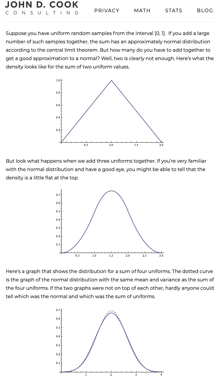
The simplest distribution to assume for resistor variation is the uniform distribution -- all values within the tolerance are equally likely and there is is no likelihood of a value outside of the tolerance specification. If you have a string of resistors in series then the probability distributions sum as well, but that involves convolution. There is a pretty good explanation of it on the web (credit --site):
![]()
So the lesson here is that when you get more than 4 sums of uniform independent random variables they can be treated just like normal probability distributions with mean, variance and standard deviation.
But that's not all. When you add resistors together you add their variances. Then the standard deviation of the sum of resistors reduces by the square root of the number of resistors: SDsum = SD/sqrt(n). That is the theory behind using 49 resistors to make a 1:25 resistor divider. My fat finger says that the standard deviation of the divider should reduce by sort(49) = 7. Roughly 0.014%.
Monte Carlo to the rescue:
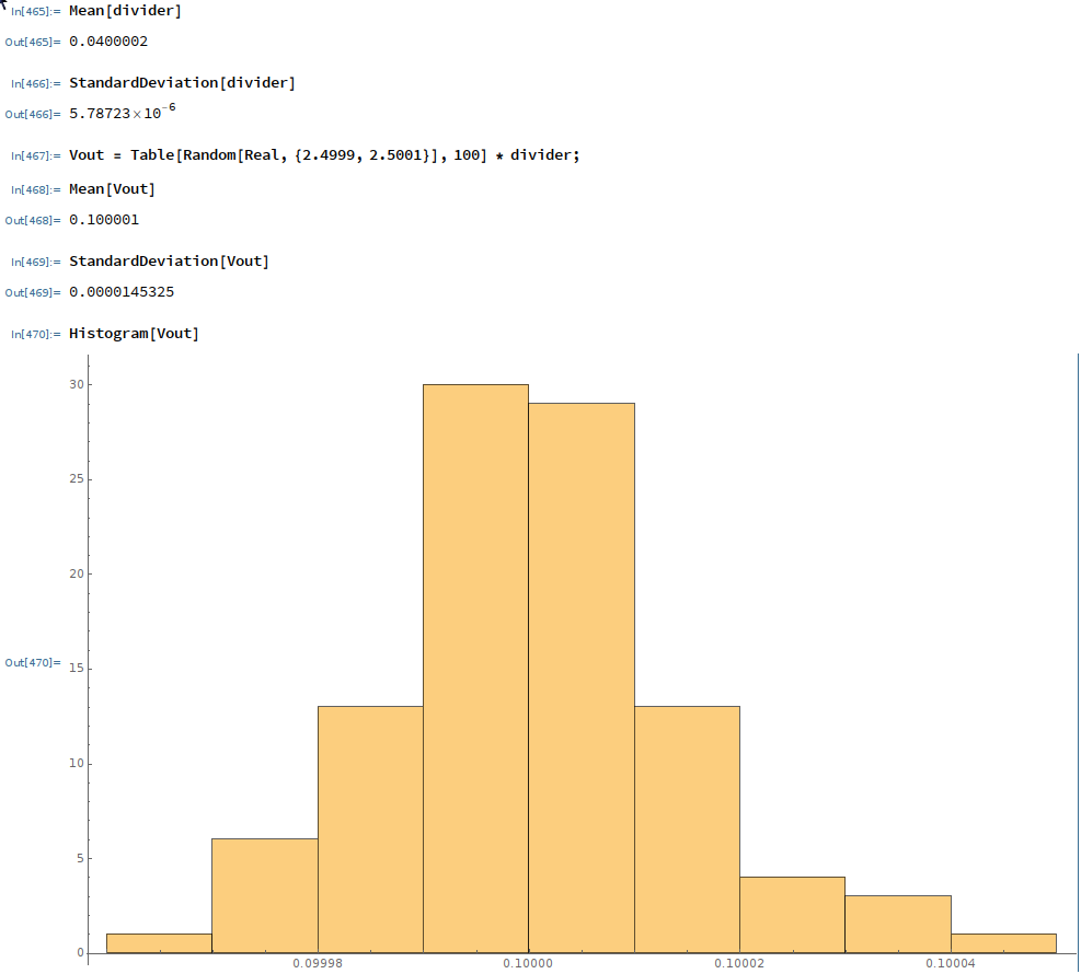
I created a Monte Carlo simulation in Mathematica to perform 100 experiments to simulate the expected value of the resistor divider. I will upload the Mathematica notebook file to the files section of this project. Each resistor was given a uniform probability density between 0.999 and 1.001 and a list of 100 random values created for each resistor. The the resistor divider function was calculated 100 times to yield a list of the divider output values. I also assigned a ±0.1mV uniform distribution to the 2.5V reference voltage to include it's expected variation. Here is the final resulting mean, standard deviation and histogram:
![]()
There is better than a 50% chance that the output voltage will lie within 10µV of 100mV. It looks like the result is pretty close to a normal density function to me.
Precision Voltage and Current Reference
A little something to check your digital multimeter accuracy occasionally.