20161116:
Just to be sure the kids understand, and to help one kid who was sick last time, let's redo the charge pump expermient. This time, with screenshots and more bugs.
Let's start with the oscillators : the classic 74HC04 provides 2 inverters, then we hook a resistor and a capacitor. By now, the kids should do this circuit without any difficulty :-)
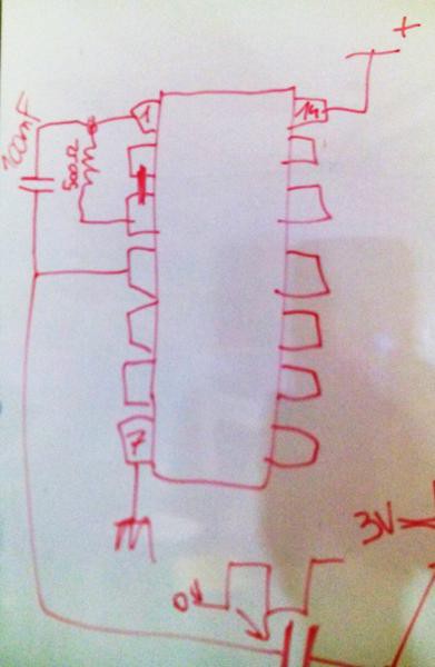
What are their value ? I have set the goal to 10KHz. A previous workshop has shown that the frequency is about 1/2RC and we have C=100nF. Let's compute the resistance...
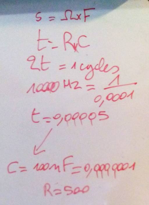
Some whiteboarding later, I come up with 500 Ohms. I can find 510 ohms in my stash of resistors so let's go. We get about 8KHz, that's -20% of the goal but pretty close, considering the other unknowns.
There's a problem though : of the 3 circuits that were assembled, 2 showed problems as they would not oscillate. The reason is not clear, bad capacitor ? Maybe a too low resistance ? (I don't have smaller capacitors at hand)
The behaviour is odd, as the scope shows a small burst of activity then the trace turns flat, mid-point between 0V and 3V.
So we focus on the only circuit that seems to work.
We connect a 1µF ceramic capacitor to the output and connect the other electrode to the scope probe.
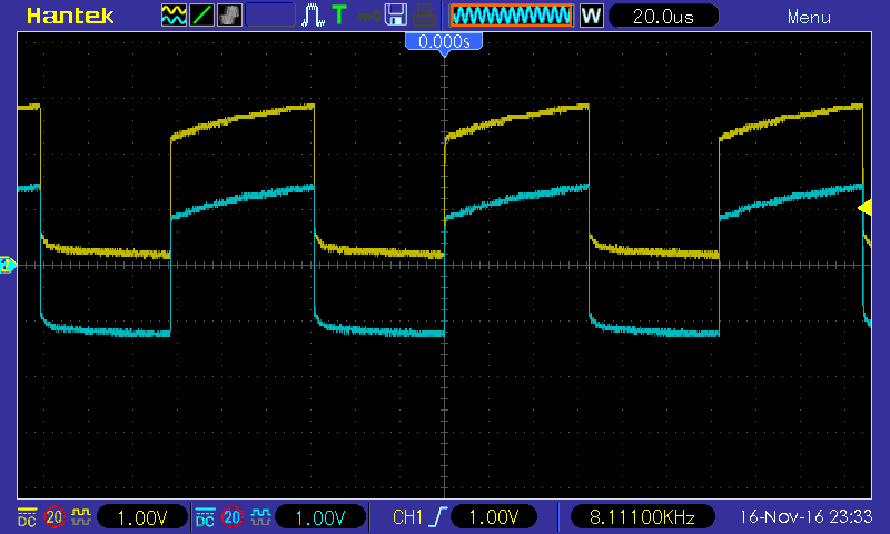
The blue trace is initially a copy of the original yellow square wave but it quickly drifts (in about one second) toward -1.5V/+1/5V
This is explained by the capacitance of the scope probe: 1µF × 1M Ohms = 1second
Cue in discussion about low-pass, high-pass, time constants and what if we set the probe impedance to the 10× mode :-)
Then let's introduce a diode : current passes in one direction but not another. Tthe diode is connected to the +3V rail and the passing direction is outward the rail.
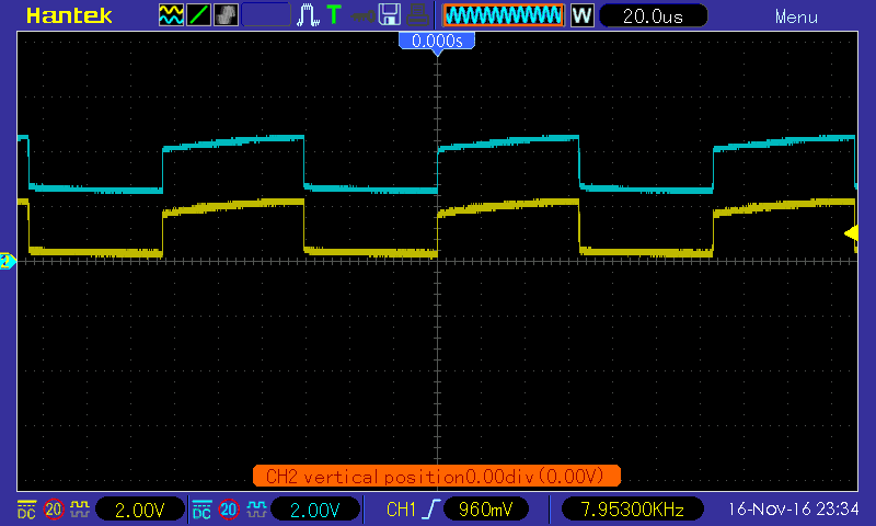 The trace has shifted upwards, the capacitor's electrode is at a higher mean voltage than the power supply.
Now, let's see with the diode connected to 0V:
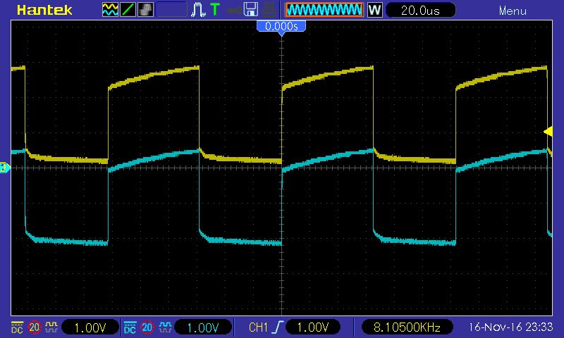
The waveform has shifted below 0V, but there is still a part that reaches 0.7V, which is the "drop" of the diode. The output voltage now reaches -3V +.7= -2.3V (this was not apparent in the previous ss because of a bad setting of the 0V level)
Now, let's add the 2nd diode and a large capacitor. Oooops, it seems to overload the 74HC04 which stops working, so let's use only 1µF.
We measure the generated voltage : with a step-up configuration and 1µF, that's 4.74V. When adding a 150K resistor load in parallel with the filter capacitor, that's 4.54V, or a 200mV drop. From there we can calculate the impedance of the generator and estimate the drop with other loads (approx 1mV/Kohms, or 1M Ohms of impedance...)
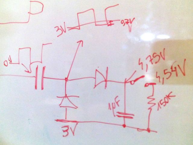
It's not efficient, but advantageous to generate very high voltage when cascaded.
Discussions about diodes lead to other applications, in particular the antique keyboards, and diode matrix ROM (oh, wait, a common subject these days :-D)
From there, how does one creates a diode ROM ? It's a matter of decoding. What can it be used for ? Let's say, a 7-segments decoder :-)
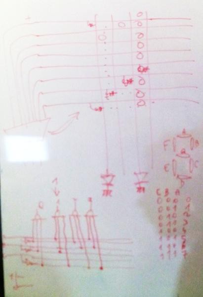
How does one decode the ROM ? it's another matrix, but with AND gates this time. Very easy to design on Minecraft, once you know how to copy-paste an element :-D
Back to the proto boards and actual (N)AND gates. The simple N-MOS inverter is shown again, and a second transistor is added to prevent it from conducting current to 0V : that's how we make a NAND.
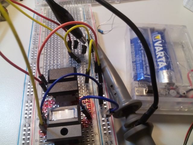
If the transistors are in parallel, it's a NOR.
Considerations about complementary MOS circuits are discussed : less power draw, faster, but at this time we're happy with a pull-up resistor. We measure the rise time (when the button is released) at about 400ns : that's slow but we don't need to run at Megahertz speeds...

 Yann Guidon / YGDES
Discussions
Become a Hackaday.io Member
Create an account to leave a comment. Already have an account? Log In.
For the record, I first discovered this circuit on the #Charleplex Xmas Tree without uC project. I knew for decades about the HC14 oscillator but the HC04 version puzzled me. It has found use in the #DYPLED where I was conscious about power draw so there is a significant resistance. But during the workshop, which does not take place in my own workshop, I had to adapt... Maybe it would have been interesting to study how capacitors behave in series and parallel :-D but all I had was 100nF.
Are you sure? yes | no
Is this a phase-shift oscillator? I at first suspected a relaxation osc, but that would more likely be a 74HC14 (Schmitt trigger) and only one gate in the loop.
Are you sure? yes | no
It is a sort of derivative from a relaxation oscillator, the HC04 is a HC14 without hysteresis and the 2nd gate and connections create the hysteresis.
Are you sure? yes | no
There is an interesting section on problems with relaxation oscillators built with two 'HC04 gates in the 3rd edition of the Art of Electronics (p.426-427). I have to run now, but I'll draw the circuit they suggest in a bit, in case you don't have the book.
Are you sure? yes | no
I don't have that book :-)
Are you sure? yes | no
They recommend this circuit, saying that the speedup cap at C2 is necessary for reliable operation.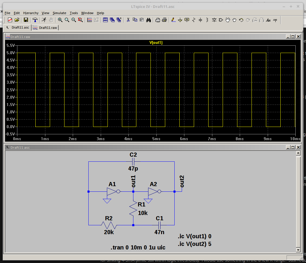
Are you sure? yes | no
OK I start to get it : A1 is the oscillating gate, biased toward Vcc/2 by the resistor network R1,R2
I'm puzzled about the ratio, though, I would have swapped their values. But the resistor network would provide some hysteresis, which C1 will overdrive with a pulse...
C2? why is it necessary ?...
I prefer the 1R 1C oscilator :-)
Are you sure? yes | no
The book says that C2 is required as a speed-up due to slow transitions of A1 from capacitive loading. They mention bad edges and parasitic oscillations at around 100 MHz. The also note that the original circuit (without C2) was listed in the 74HC4060 datasheet. I haven't looked at all the various manufacturers but this one has the circuit:
http://cache.nxp.com/documents/data_sheet/74HC_HCT4060_Q100.pdf?page=15
it may be that other datasheets for this part provide some more info.
Are you sure? yes | no
The resistor determines the charging/discharging current, so peak is like 5V/500 ohms = 10mA. The part is for sinking 4-5mA (while still within logic thresholds). I would use something in the a few K range. Just reduce the capacitance if you want higher frequencies.
Are you sure? yes | no
This was one of my hypothesis because when I used the output to drive the other capacitor, the circuit would collapse easily. But
a) it seemed to work in some cases
b) I didn't have smaller capacitors
c) it didn't work better at 1K
Anyway, it's good to know for next time :-)
Are you sure? yes | no
Using a larger R means that the efficiency would be slightly better as you are wasting less energy charging and discharging a smaller value caps.
Are you sure? yes | no
N.B.: I use 3V (2×1.5V alkaline batteries) so the current is in the 6mA range, just on the edge of 5mA... What a coincidence.
Are you sure? yes | no
The driver impedance would be higher at lower voltages. The actual charging/discharging voltage is a fraction of Vcc as these are running closer to their thresholds.
Are you sure? yes | no