Theory of operation
Much of this is abbreviated from the TS50 project so you can get more detail there. The sine bridge is an implementation of Direct Digital Synthesis (DDS). The controller produces a set of fixed frequency, duty-cycle varying drive signals connected to an H-bridge that send the modulated high-voltage square wave thru a set of LC filters to produce a low distortion 60Hz sine wave.
The bridge operates at 48kHz which allows for a sine pattern with 200 discrete values per quarter sine. Each value represents the time equivalent of a sine angle from 0 - 90 degrees. The controller ‘plays’ the pattern forward & backward for each half sine and then repeats the process for 180 - 360 degrees.
Electrically, the H-bridge functions a bit different from one driving a transformer.
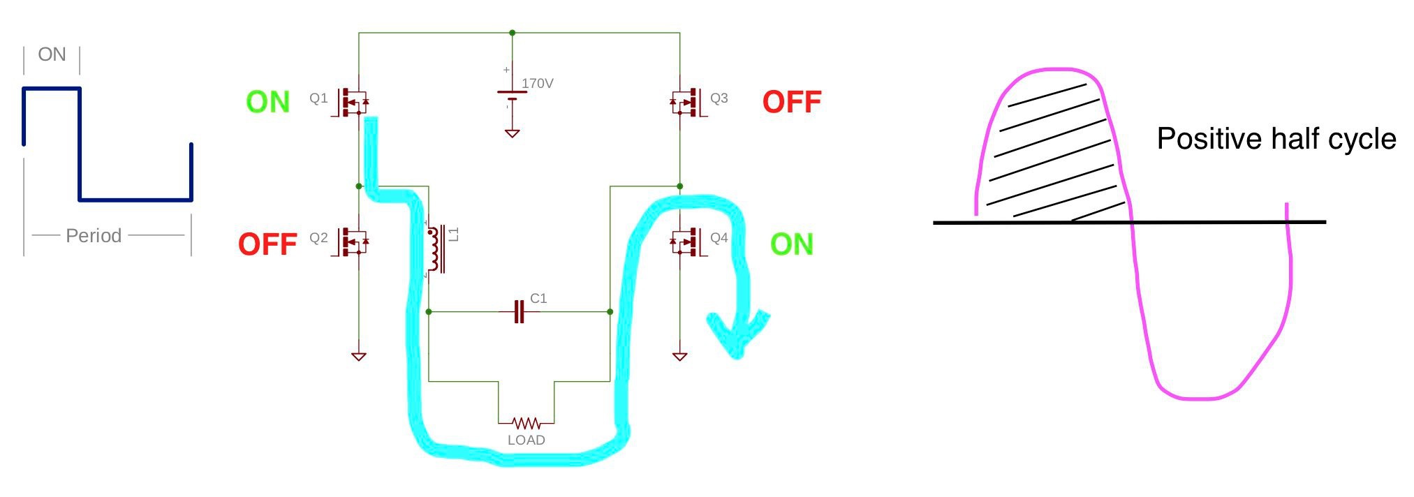
During a given half cycle the low-side switch Q4 remains on (no switching) which connects the load to the high voltage supply negative pole. When the high side switch, Q1, is on, inductor L1 is charging and current flows thru the load to the negative supply pole.
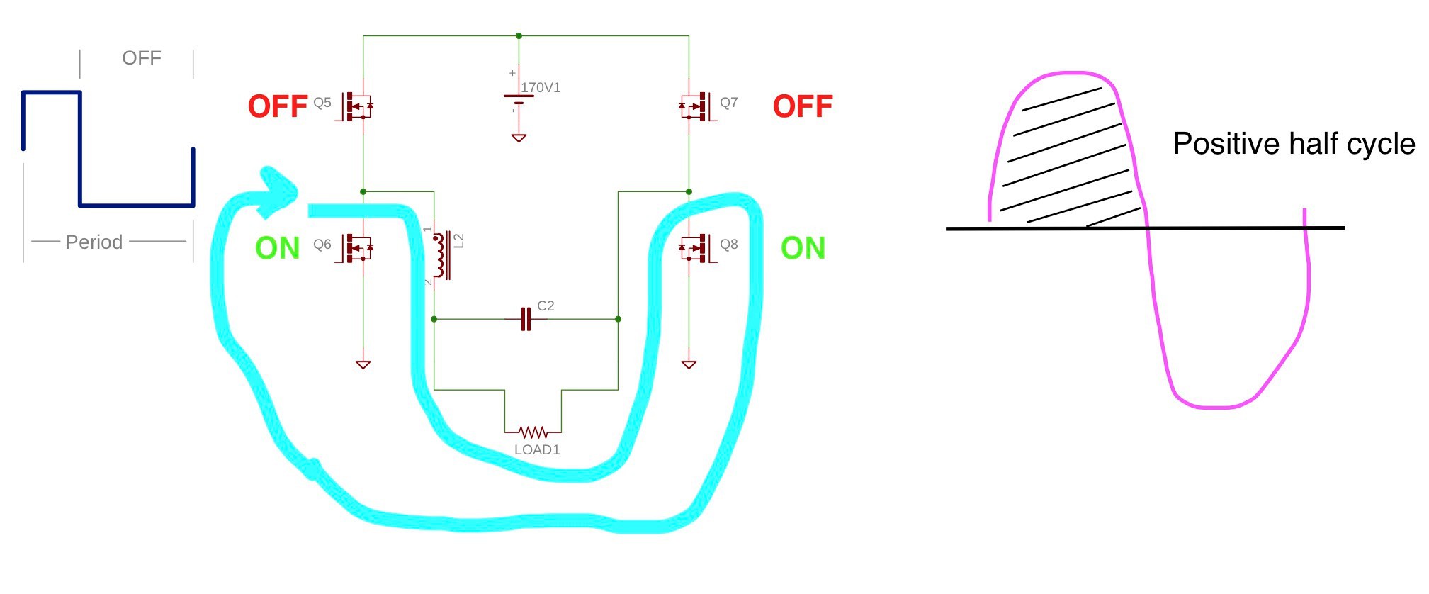
When Q1 turns off L1 reverses polarity to maintain current flow. To close the circuit Q2 turns on. Current no longer returns to the high voltage supply but instead uses the ground plane to flow thru Q2 and return to the negative node of the inductor.
This process repeats for one half sine cycle and then reverses with the other half of the bridge performing the switching. Although the diagrams only show a single LC filter, the TS350r1 has one for each leg and functions the same. The architecture could be thought of as two alternating and parallel buck converters.
Power Supplies
The sine section has three supplies. The Vcc supply is derived from a full-bridge rectifier on the transformer auxiliary winding and provides 13V via LDO U403. Vcc powers the gate drive and bootstrap circuits. Vdd provides the 5V logic supply for the controller, temperature sense, and communication isolator. An unregulated tap is also taken directly from the rectified transformer auxiliary that is used by the controller as a proxy for the high voltage supply (and is spared the dissipation of a resistive voltage divider).
The high voltage supply consists of a full bridge rectifier and powers the H-bridge. Heat sinking is required, so to conserve space dual common anode/cathode TO220 packages are used. Three lower-value capacitors are placed in parallel to provide bulk capacitance. This allows for a lower maximum mounting height with no trade-off in PCB space based on the layout. The cost is just slightly more for three smaller vs. one big one.
With a two stage inverter design such as this, more capacitance for the high voltage supply isn’t necessarily better. It costs more, takes up a lot of space, and can complicate short circuit hardening for the H-bridge. It also puts more strain on the boost stage, both at startup and to keep it charged when under heavy load. This design’s transformer has poor regulation so the bulk capacitance helps reduce the sag to keep the minimum AC RMS voltage a bit higher than it would otherwise be.
Controller Card
The controller card houses the gate drivers and MCU. It’s physical design is very similar to the inverter: right angle 100mil pins, vertical mount. This allows for a more compact design and small gate drive loops.
The gate drivers are the same component that is used for the inverter. And, as with the inverter section they allowed for minimal components to manage parasitics. Even though the controller to gate drive signal lines behave as a lumped system, the traces lengths are matched to ensure clean timing.
The MCU’s main job is DDS pattern generation which includes a crude form of voltage regulation. Secondarily it monitors the bridge temperature and turns the AC output on & off in response to assertion of the CMD pin.
The DDS pattern generation is performed with a mix of MCU peripherals and firmware.
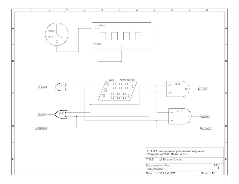
The bridge frequency is provided by Timer2 and drives PWM5. PWM5 drives the Complementary Waveform Generator (CWG1) which is configured as a half-bridge (HB). In HB mode the ‘A’ line is high when PWM5’s output is high (the duty cycle) and the ‘B’ output goes high at the end of the duty cycle and remains on for the duration of the period. CLCs 1-4 steer the CWG’s output to the side of the bridge that’s active. The ‘ENABLE’ tags determine which side is active.
To properly generate the sine, the duty cycle must change each period. A firmware interrupt triggered by Timer2 retrieves & loads the next duty cycle value to PWM5’s registers. At 90 degrees the pattern is loaded in reverse (high->low DC). At 180 degrees the bridge direction is reversed by reversing the ‘ENABLE’ pins, and the DC pattern loading process repeats. All of this must happen in less than one period (20.833uS) and leave sufficient time for some foreground processing.
Hence, the MCU must be run fast and is a limiting factor in the pattern generation’s resolution. That said, testing has shown that 200 samples per quarter sine is quite sufficient for a low distortion sine. The only advantage of higher speeds is a reduced output inductor but at the expense of more memory and a faster processor. Since the sine pattern is an array loaded in program flash care must be taken to minimize access times since it is much slower than SRAM. This is why each array element is first copied to SRAM (of course with enough SRAM the entire array could be copied there first).
The DDS algorithm also provides course regulation of the AC output voltage since the inverter stage doesn’t regulate. Because the MCU doesn’t have the processing power to dynamically calculate the angle timing, the DDS pattern is selected from a fixed array to keep the output voltage within 5V RMS of the nominal output. The resolution is limited by the resolution of the sine pattern and the available flash.
Array selection is done using a simple PI control loop that executes in the foreground. The rectified auxiliary voltage is sampled using the ADC and compared to a reference from which the proper array is selected. Array patterns are switched only at the start of a new sine (0 degrees) to prevent distortion.
The foreground loop starts the bridge when the Run pin is set TRUE. Once running the Acknowledgement pin is set TRUE. When the Run pin is set FALSE the bridge stops at 0 or 180 degrees which can take up to 8.333mS. The intent of this is to provide a soft (0V crossing) off for connected equipment (zero current crossing would be better but isn’t possible since the AC current waveform isn’t monitored).
The MCU also monitors the temperature of the bridge in the foreground loop using comparator C1 and the DAC. If the temperature is above the Hot threshold the bridge will not start. If it is running it will continue to do so but set the Acknowledgment line FALSE and allow the main controller to determine if operation continues. if the temperature exceeds the Overheat threshold the bridge is stopped.
Bridge
All high current & high speed switching generates a lot of EMI. Keeping the current loops as small as possible helps. When heat sinking is required, as in this design, faraday screens help reduce common mode noise on the supply. High voltage switching further complicates the layout. Placement of the ground plane must ensure short return paths but avoid placement under the switching nodes to avoid additional common mode noise thru the parasitic capacitance of the PCB.
This design does a better job addressing these issues than its predecessors but the switching loops (bridge to LC filters) is still too big. Ideally the LC filters would be placed on the opposite side of the PCB opposite the bridge. This would provide a very small switching loop but would require a layout & size dimension that conflicts with other objectives in this design. Note that the mounting edges of the PCB use a via fence to contain EMI. The bottom edges of the PCB ground plane are also exposed to ensure the metal enclosure is grounded so it can function as a faraday cage.
This switching and LC arrangement works well for an isolated (non-grid connected) inverter. It’s reasonably efficient because all switching is handled by the MOSFETs (as opposed to the body diodes or external anti-parallel ones) and the dual LC filters provide a very low distortion sine.
But it does have significant drawbacks. It can’t be used in a grid connected system because the switching arrangement would create a short if operated with a supply voltage less than that of the grid. Second, the dual LC filter arrangement adds a lot of bulk and cost. Alternate designs perform all the switching behind a single LC filter and achieve good results. A single LC could be used on this too - in fact the TS50 does just that. But this significantly increases the radiated EMI because one leg of switching is done thru the entire AC loop.
Speed Matters
But not in the way you’re probably thinking. The semiconductor OEMs marketing folks will have you thinking that faster switching is always better - smaller inductors, more compact designs, etc. But faster brings with it a more complex design that is less forgiving. Note that when you get to the technical material that addresses design & troubleshooting from those same OEMs that the first recommendation for a parasitic problem is, wait for it, - slow it down!
The original MOSFET I selected for the sine bridge was the STP46NF30 from ST. I selected it for its speed, low Rds(on), and generous SOA which is necessary to survive inrush and equipment shorts in inverter applications. But, as I began load testing, the low side switches would instantly fail with an applied inrush or a load exceeding a few hundred watts.
Here’s a trace of the scene of the accident.
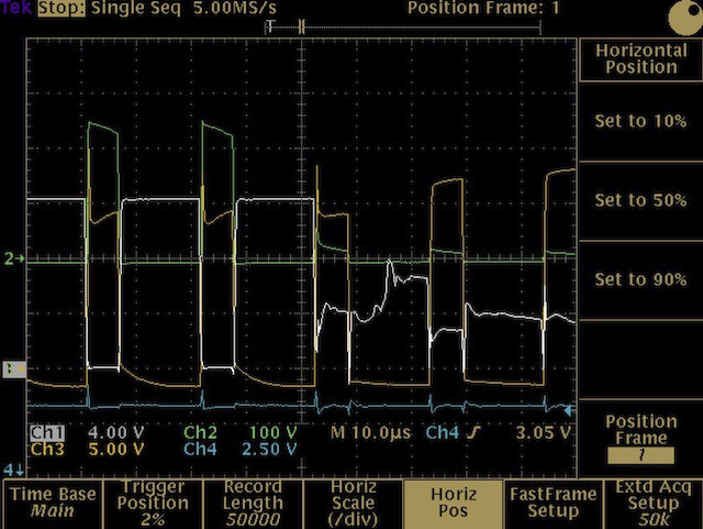
CH1 is the low-side gate drive, CH2 is the center of one leg of the bridge (e.g. output to inductor), and CH3 is the same side high gate drive. You can see the gate break down and subsequently short the bridge. I spent weeks on it. It defied all logic: the high side transistors had all the voltage stress and they should have been the casualty. But not a single one of them failed. After finally abandoning the idea that it was an SOA issue I began searching for more subtle parasitics.
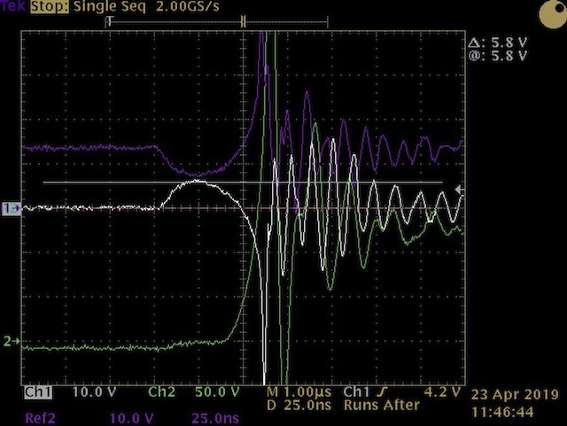
This trace is the detail behind the prior trace at the moment of failure. CH1 is the low side gate drive, CH2 is the center tap of the bridge. Notice the bump highlighted by the cursor - about 5.8V over 50nS. That bump is caused by the voltage drop across the low side gate resistor due to the high dv/dt of the high side MOSFET turning on and the resultant charging of the D-G capacitance on the low-side switch. Now, let’s look at the MOSFET’s gate & switching characteristics.
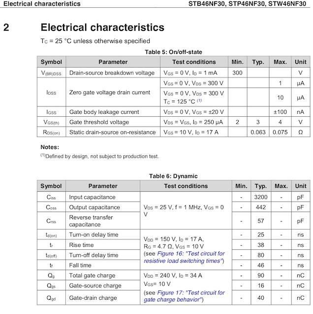
The minimum gate threshold is 2V - a poor margin for a high power design and something I should have picked up on during selection. Note the turn-on delay of only 25nS and a rise time of only 38nS. This thing is too fast for its own good. I tried lowering the gate resistor (beyond safe limits) and even a small shunt capacitor G-S but was not able to eliminate the problem; I would have to select another transistor.
I fell back to a variant in the same family that I used on the prototype but selected one with a much better D-S rating: the Fairchild FDP20N50.
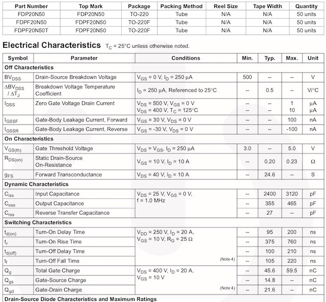
It’s slow and has an Rds(on) over three times that of the STP46NF30. But its reverse transfer capacitance is half the ST and has a better gate threshold margin. Also note the differences in total & G-D charge Here’s a trace of the same event with the Fairchild MOSFET.
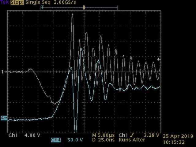
No gate bump. Note that the dv/dt of the high-side turn on is just as high the the Fairchild as with the ST. That’s because it’s induced by the inductor reversing polarity and not the switching speed of the high-side transistor. This is confirmed by the measured dissipation of the sine bridge. The thermal model for the FDP20N50 showed switching losses of over 12W but long runtime @ max load tests never got near that. I had to add a derating constant to the model to match observed results. And I haven’t gotten one to fail in destructive testing.
So why such a dramatic difference? I’m no expert on MOSFET construction but I have learned that it is very important to not only understand the parameters but to also how it relates to the transistor’s construction. Putting all the parameters together: switching speed, gate charge, gate threshold, D-S rating, etc., along with the performance graphs helps to do this. And carefully consider how the device will operate in the design and all of the stresses that adjoining components will place on it.
Last, make sure you have bench equipment fast enough to analyze high speed events. This design’s operating frequency its only 48kHz but switching events are much faster. Note the timebase in the last two traces - 25nS with a sampling rate of 2GS/s. These events weren’t even visible at 100nS. I was fortunate to have equipment fast enough to catch it.
Discussions
Become a Hackaday.io Member
Create an account to leave a comment. Already have an account? Log In.