Mark Omo
-
Probe-Scope Frontend Divider: A Dive into Black Magic
07/07/2019 at 04:14 • 0 commentsThe frontend (input) divider of an oscilloscope is one of the most critical components of the whole system. It needs to attenuate the incoming signal a precise amount over a very wide frequency range; in the case of the Probe-Scope, from 1 Hz to 50 MHz or more. This requires careful consideration of the parasitics on the PCB.
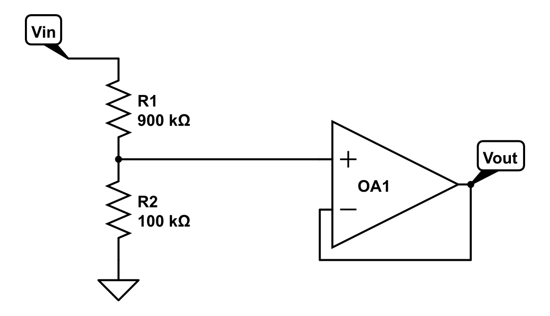
First, it’s important to know what an ideal frontend looks like. It’s a resistive divider with a buffer, with a constant divide ratio vs. frequency:
![]()
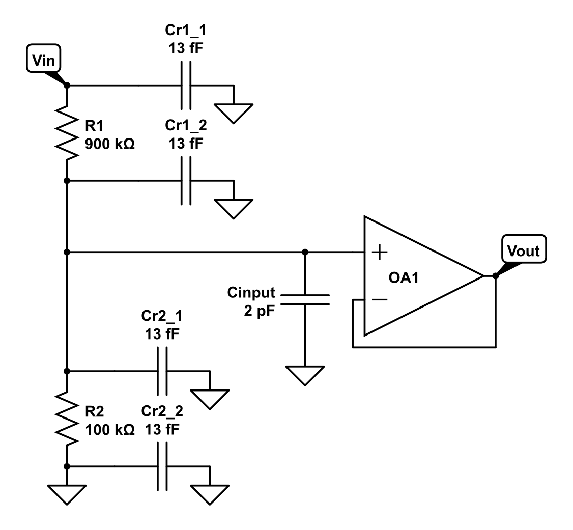
However, in the real world, things are not as simple as they might seem. Every component has what are called “parasitics”, i.e. parasitic resistance, capacitance, and/or inductance: these are the result of unwanted interactions between elements. In the case of our divider, parasitic capacitance has the largest effect on the system. The first major contributor is the capacitance of the op-amp’s non-inverting input. We are using the Analog Devices AD8055 for our buffer, which has a typical Input Capacitance of 2pF. The effect of this capacitance on the circuit can be drawn in the schematic:
![]()
The next elements that contribute capacitance are the resistors themselves. The pads on the PCB that they sit on form parasitic plate capacitors with the ground plane below:
![]()
The formula for a plate capacitor is C=(k ϵ0 A)/d. Because the size of each pad is 700μm by 800μm, assuming a standard PCB thickness of 1.6mm, as well as a dielectric constant of 4.2, that gives each pad around ((4.2)(ϵ0)(0.56mm^2))/1.6mm=13fF of capacitance. Here’s what those look like in the schematic:
![]()
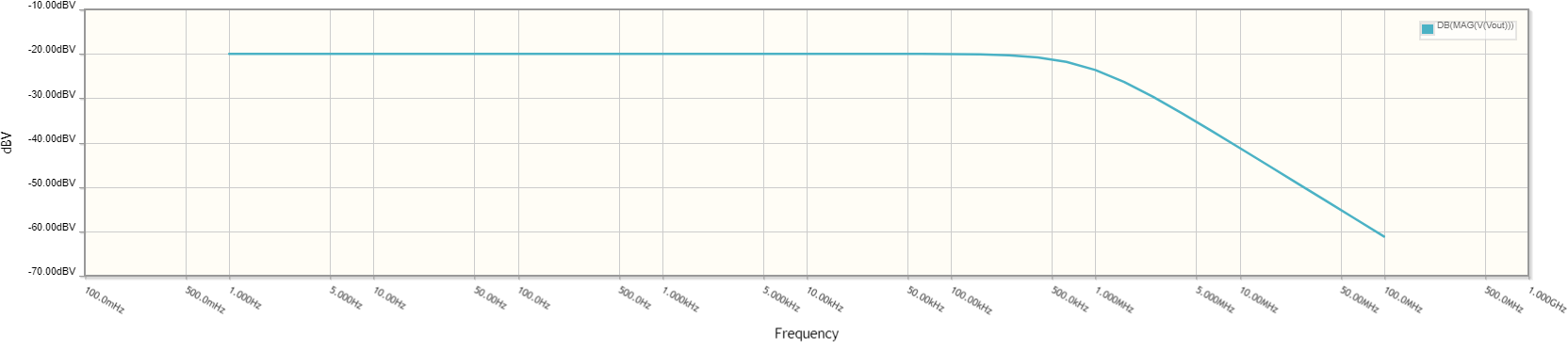
If we analyze the frequency response of that circuit, it’s clear that it won’t work for our target bandwidth of 50MHz. The parasitic capacitors form a low pass filter with the resistors, giving the front end a response that’s far from ideal:
![]()
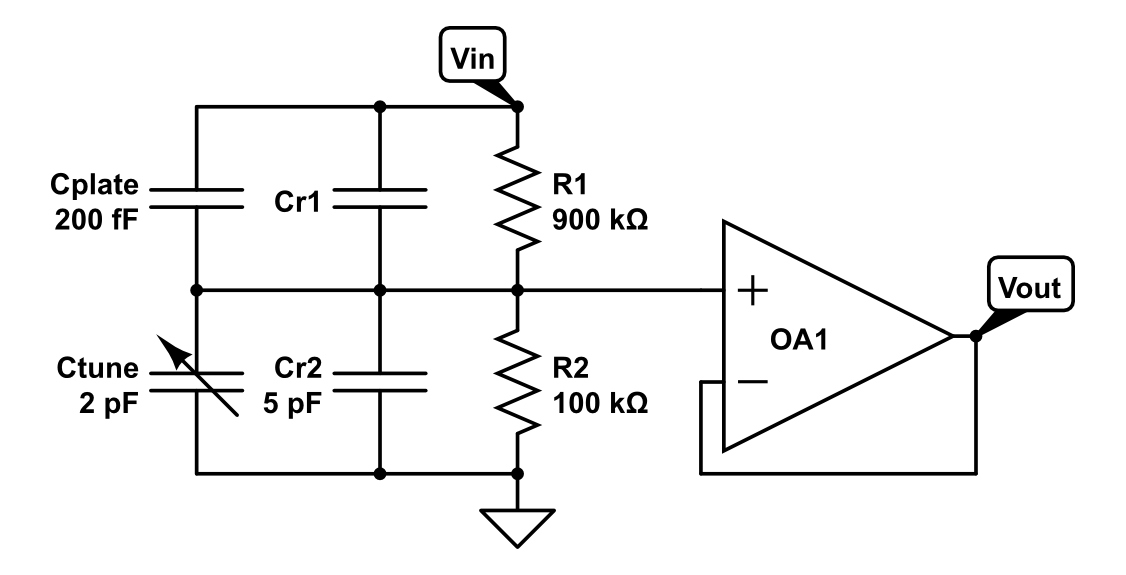
So, since that doesn’t get the system where it needs to be, we need to compensate for it somehow. If we simplify the system, we see that there are two critical values, the capacitance across R1 and across R2 (where CR1 includes other parasitics, putting its value is in the 0.1pF range):
![]()
For the divider to have the same ratio for all, frequencies C_R1 needs to be one tenth the value of C_R2, which means it needs to about 0.5pF. Because the parasitics are not well controlled we need to add a tuning cap, but there’s a problem: tuning caps in the 0.5pF range are VERY expensive (in the $20+ range), while inexpensive turning caps start in the 2pF range. To accommodate an affordable tuning cap, CR2 would need to be in the 20pF range, however that would result in the whole frontend having a high capacitance.
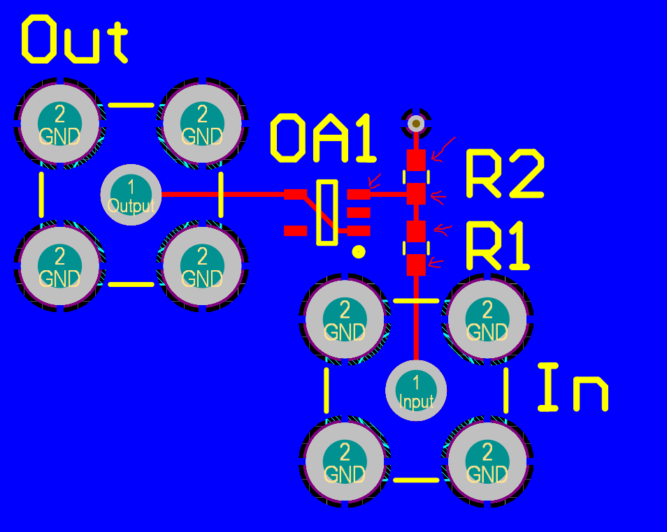
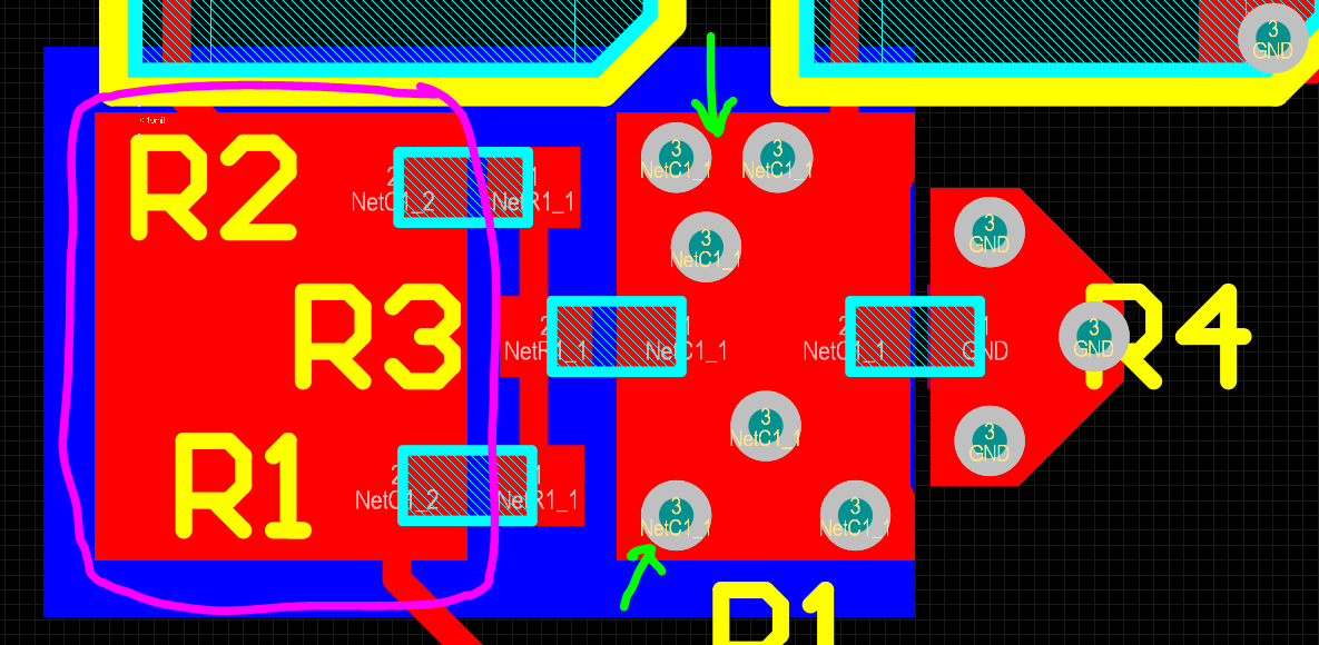
Instead, we can intentionally add some parasitic capacitance to R1 and add a 2pF tuning capacitor to R2. This will give us the desired response and a small input capacitance, without driving up the cost. We achieve this by extending the node between R1 and R2 as a plane on the bottom of the PCB, and placing another plane above it that’s connected to the top of R1 (Vin). Below is a screenshot of the layout of the Probe-Scope input divider, where R1, R2, and R3 form the top resistor (R1 in the schematic, it ends up being a weird value hence the multiple standard resistors) and R4 forms the bottom (R2 in the schematic). The area circled in pink is the top plate of the parasitic capacitor, and the green arrows indicate the vias that connect the divider node to the bottom plate of the capacitor.![]()
Here’s what our model looks like now:
![]()
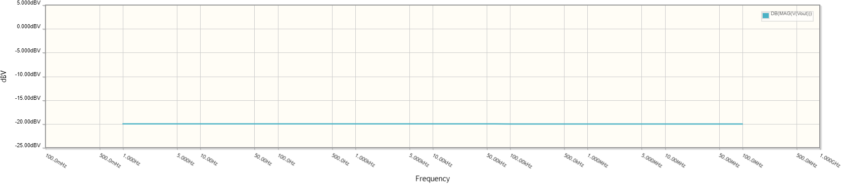
And with all that in place, here’s our ideal frequency response!
![]()
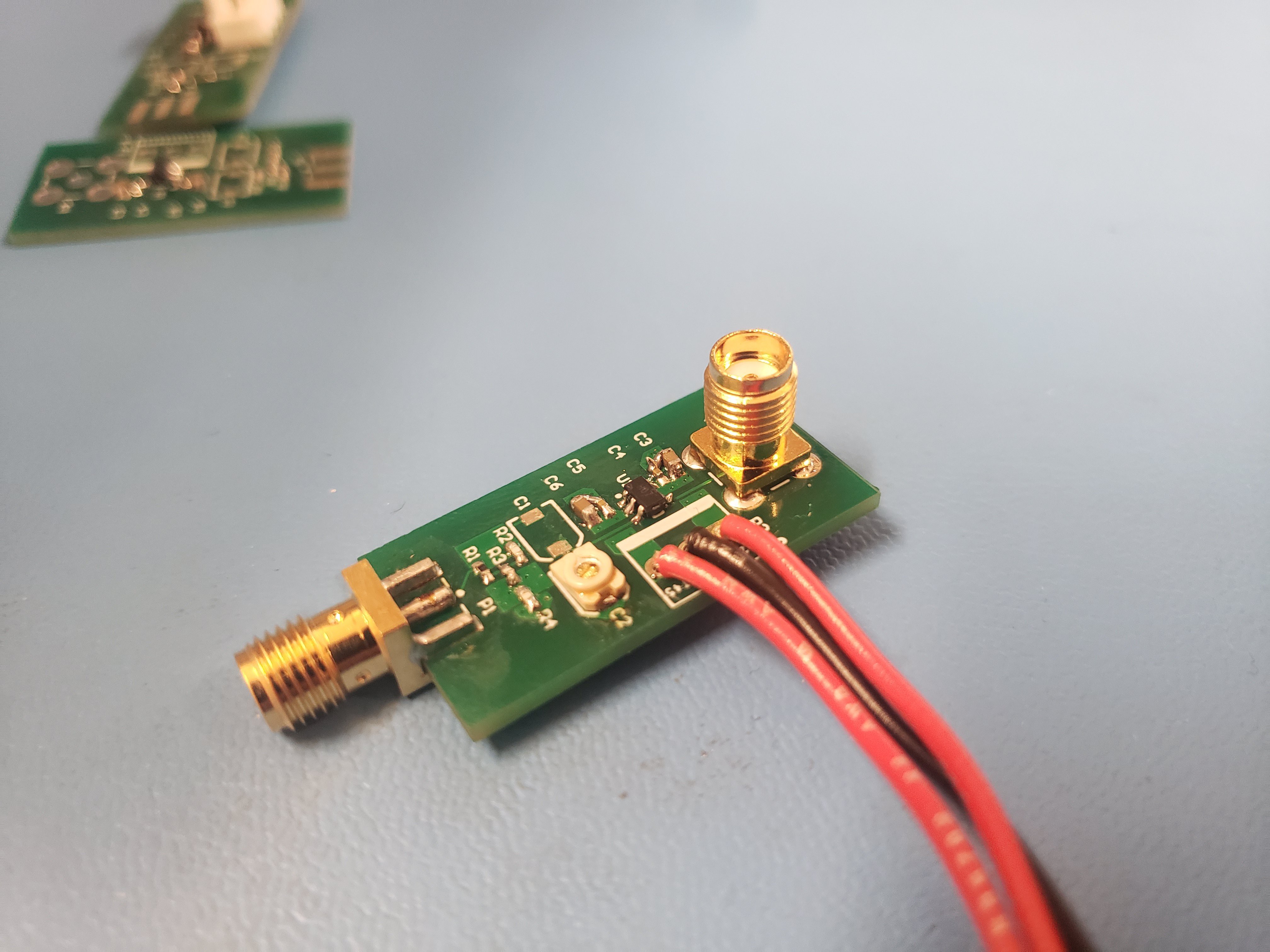
We elected to put the frontend divider on its own PCB for the first round of prototypes, rather than integrating it with the rest of the frontend so we can test each component independently.
Here’s a picture of the board, it's slightly more complex than the example presented above. A detailed post about the frontend performance will come shortly!
![]()
-
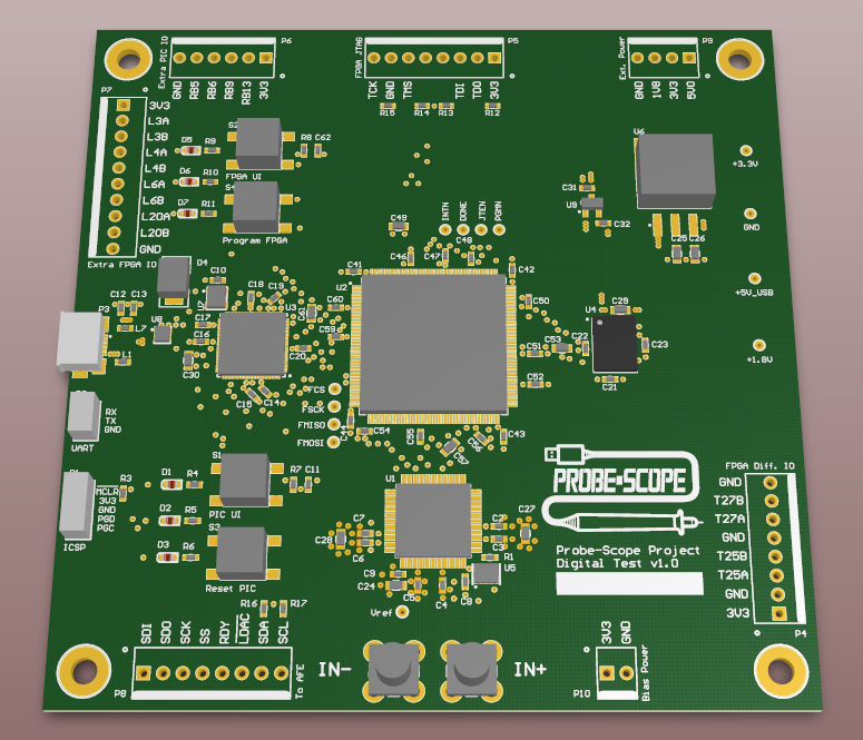
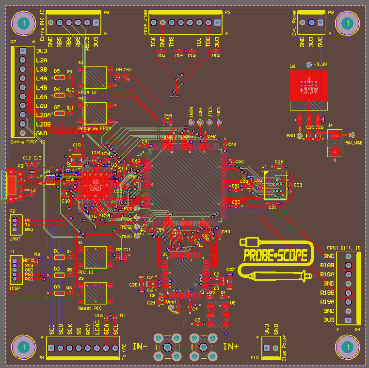
Digital Test Board
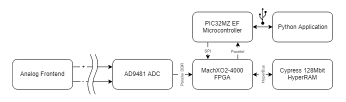
06/29/2019 at 23:58 • 0 commentsIn a similar fashion to the Analog Input Test Board, we created a Digital Test Board, so that we could compartmentalize development efforts and get both halves of our system up and running at the same time. The Digital Test Board contains the Analog Devices AD9481 ADC and everything needed to get data out of it and on to a computer over USB: to accomplish this it uses a Lattice MachXO2-4000 FPGA, a Cypress S70KS1281 self-refreshing DRAM, and a Microchip PIC32MZ2048EFH MIPS microcontroller.
![]()
The ADC is clocked by a Microchip DSC1103 250MHz LVDS MEMS oscillator, and since its output is 250Msps Double Data Rate (DDR), its output clock is 125MHz. It has two output ports, A and B, each 8 bits, with A being valid on the falling edge of the clock and B on the rising edge. The data clock output from the ADC is used as the clock source for the FPGA, which has built-in DDR support on the bottom IO cells.
Once the data gets into the FPGA, it’s stored into “EBR” SRAM in FIFO mode (a hardened feature of the MachXO2), where it waits until it can get send out in blocks to the Cypress “HyperRAM” device. Also at this time, the FPGA checks the incoming data for a trigger condition. We use the FPGA’s PLL to generate a 166MHz clock for the HyperRAM, which is its top speed. Since the HyperRAM is a self-refreshing DRAM, it does have to spend some time refreshing occasionally, and we also have to reset the address when we get to the end of the memory, so we can’t just write continuously at the ADC’s output frequency. Instead we run it slightly faster and write out bursts of data, allowing for control and refreshing to occur in between bursts.
![]()
The PIC controls the FPGA via SPI (using the FPGA’s hardened SPI peripheral) and also with simple GPIO. It sets the trigger conditions for the FPGA, and when a trigger is detected, it requests the relevant slice of data from the FPGA, which will transfer it out of the HyperRAM and into the PIC via a parallel port. At the same time (since in most circumstances the PIC cannot hold all the data at once), the PIC transfers the sample data over USB to a Python application running on the user’s computer. The design data for the digital test board can be found on our GitHub, and here is a direct link to the PDF:
Our boards have finally been shipped, so we'll get them hopefully on Wednesday and build them this week.
-
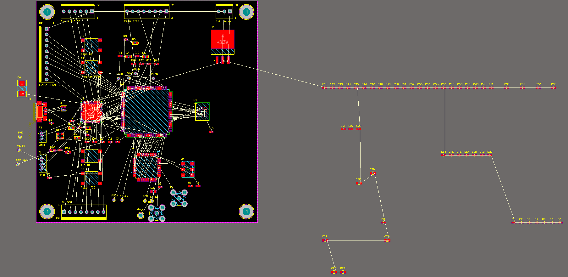
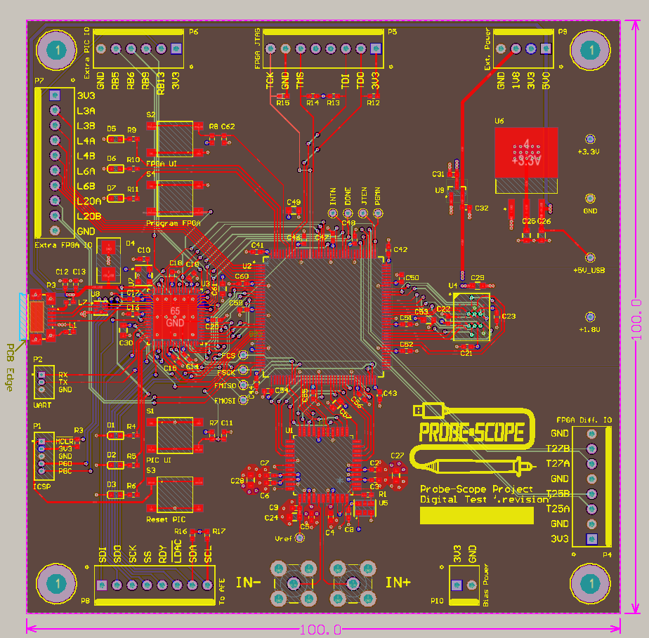
Progression of a PCB
06/26/2019 at 01:21 • 0 commentsWhile designing our Digital Test PCB (which I'll be posting about in detail in a day or two), I decided to take a couple screenshots of the board as I worked on it, thinking it might be fun to see how it comes along. In the center of the board is the MachXO2-4000 FPGA, with our PIC32MZ2048EFH processor on its left port, the AD9481 ADC on the bottom, and a 128Mbit Cypress HyperRAM on the right port.
I start by defining the board size and bringing in all the components from the schematic, then placing the connectors and major components:
![]()
The board is 100x100mm as that's the cutoff for PCBWay's lowest price. I organized everything around the FPGA since it's really the hub of all our signals. You might notice that the final version has a few more connectors - since we're in the early development phases, it's a fairly fluid process, and Mark thought of some more nice-to-have features so I just went ahead and threw them on.
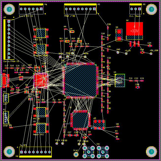
Next, I get all the decoupling capacitors next to their associated ICs (with some old-fashioned pen-and-paper action) and roughly place minor components:
![]()
Now for the "draw the rest of the owl" step, I route everything and finalize component placement. This board took me roughly 10 hours to route (very roughly, I should have timed it). I put a ground plane on layer 1 and a power plane on the bottom, so I tried to avoid those as much as possible but completely avoiding them wasn't practical. I'd have gone into a bit more detail with the pictures, but it's really just drawing lines that can't cross for hours until it's done. Here's the result:
![]()
Of course, there's always still a few tweaks to be made. I made the power test points a little more logical, moved our debug differential IO to the top port which has true differential drivers, and made a single trace going under the RAM a couple mils thinner as the manufacturer informed us that there is a wider clearance between BGA pads and other copper in the normal process (it would have cost around $400 instead of about $50!). We also realized just in the nick of time that we required the 1.8V version of the HyperRAM part in order to get the full speed which we needed, so a 1.8V rail was added for that.
So here's the final design we sent to the manufacturer:
![]()
On the final board, I'm planning to get a timelapse of the whole layout process (unfortunately none of this layout will be reusable as compactness is a priority). You can check out the board on our GitHub page, and I will be writing another post about its design and function in a couple days. Hopefully we'll have them built up a few days after that!
-
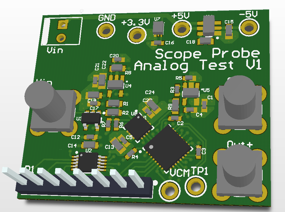
Analog Input Test Board
06/14/2019 at 04:41 • 0 comments![]()
We created a test board for the analog input section of the Probe-Scope to test the frequency response and the noise floor. This board contains the input divider/buffer, vertical offset amplifier, and programmable gain amplifier (with filters); it connects via SMA to a companion digital test board which hosts the ADC and necessary acquisition hardware. The schematic of the analog test board is shown below.
![]()
-
Introducing the Probe-Scope
06/10/2019 at 15:01 • 0 commentsAs the maker community continues to expand, there is a growing demand for entry-level tools that are affordable, and chiefly, simple. The basic tools of electronics development haven’t changed in a long time, but much like the TS100 iron made precise soldering more accessible, we aim to make signal analysis more accessible through our entirely self-contained oscilloscope and probe: The Probe-Scope. At its core, the Probe-Scope is a compact single channel oscilloscope with all the acquisition hardware contained along the cable (either in the probe body or into an enlarged USB connector, we’re still working on that detail).
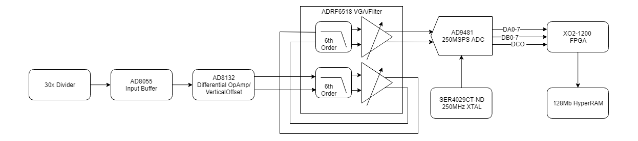
Architecture
![]()
The Probe-Scope’s architecture can be described in three sections: the input divider and buffer, the programmable-gain amplifier (PGA), and the acquisition hardware.
Input Divider/Buffer
The input signal first goes through a fixed 30x divider, the output of which is buffered by a high-speed op-amp, giving the probe a ±15V range, ±150V in x10 mode. Then the signal goes to a differential op-amp configured to sum the signal with an offset signal from a DAC, before finally going into the gain settings in the PGA. One of the most critical parts of the frontend is keeping noise low: total noise is proportional to the bandwidth that you measure over, and we’re targeting a bandwidth of over 50MHz, meaning any noise on the frontend will have a much greater impact than at a lower bandwidth. (For reference, the largest single noise source is the input resistor divider.)
Programmable-Gain Amplifier
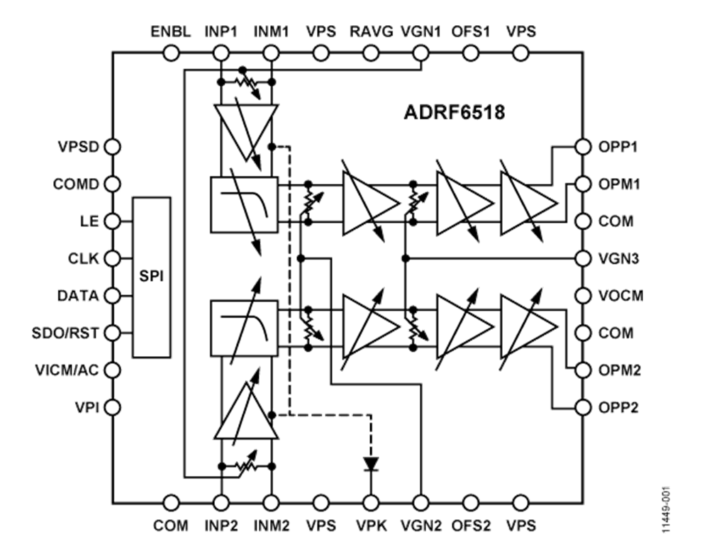
![]()
The PGA is a single ADRF6518 that contains both a programmable-gain amplifier and filter, with two identical paths. It serves two functions: boosting or attenuating the input signal in preparation for the ADC and performing anti-aliasing. We take advantage of the ADRF6518’s two paths by looping the signal through twice, to achieve a very sharp anti-aliasing filter response. The filter’s response is effectively a 12th order filter (from two sequential 6 pole filters), providing 240dB/decade of rejection and allowing us to reach 50Mhz of (noise free) bandwidth with only a 250MSps ADC.
Acquisition
To sample the signal in our digital section, we have selected the AD9481, an 8-bit 250MSps ADC which has an ENOB (equivalent number of bits) of 7.9 bits, providing high performance. The ADC’s output is fed into a MachXO2 FPGA, which in turn stores it into a 128Mb HyperRAM, providing 16Mpts of memory. The triggering is all digital, handled by the FPGA.
Not shown in the diagram is a PIC32MZ EF which is also connected to the FPGA. After all the data is acquired for one trigger, the PIC32 reads it off the HyperRAM (through the FPGA) and then transmits it over USB to a PC for display. The PIC32 also controls the vertical offset DAC, communicates with the ADRF6518 via SPI, and sets the triggering on the FPGA.
60MHz Bandwidth 250Msps Probe-Scope
The Probe-Scope is an open source 60MHz 250Msps oscilloscope probe with all guts built right in, that plugs directly into your PC via USB