-
A Word From Our Sponsors
08/26/2019 at 17:08 • 0 commentsWe'd like to thank our two sponsors for this project:
![]()
PCBWay, who was the manufacturer for all our PCBs and who also did the assembly for the final boards, kindly offered us a substantial discount on our final PCBAs. They have consistently made high quality PCB(A)s and have been responsive and pleasant to work with, and their low prices have helped us keep costs down on the job and made many personal projects (like this) affordable that wouldn't have been otherwise.
![]()
Marcus Engineering, LLC, the mutual employer of all our team members, paid for our final round of boards, which we're very grateful for since these were quite expensive in prototype quantity. At Marcus Engineering we provide high-end electronics engineering and product development services covering the entire product development lifecycle; we are based in Tucson, AZ.
-
Probe-Scope Video
08/25/2019 at 13:58 • 0 comments -
Dear Judges…
08/25/2019 at 10:24 • 0 commentsWe know you have a lot of projects to get through, so we’ve put together this brief on our project as it pertains to the criteria of the Hackaday Prize.
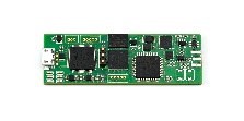
First of all, what is the Probe-Scope? It’s an open-source oscilloscope running at 250Msps with 60MHz of bandwidth, in the form factor of a cable; imagine you cut the BNC end off of an oscilloscope probe, and replaced it with a USB port: that’s the Probe-Scope.
i. Is this a unique solution to a particular challenge facing the world today?
The Probe-Scope is an innovation in the world of oscilloscopes, bridging the gap between the current low cost, low performance open-source oscilloscopes, and professional, expensive, closed-source oscilloscopes.
The Probe-Scope grows as you grow, giving you as many channels as you have USB ports; it’s almost infinitely expandable to tens (or more!) of channels. We are shooting for every channel to cost around $100, putting it on par or even cheaper than the commercial closed-source solutions out there today.Closed-Source Comparison:
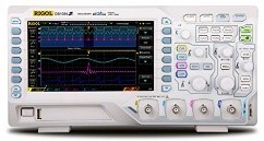
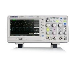
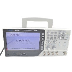
Scope Model Probe-Scope RIGOL DS1054Z Siglent SDS1052DL Siglent SDS1202X-E Hantek DSO4102C ![]()
![]()
![]()
![]()
![]()
Price/channel $100 $88 $130 $180 $145 Open Source? Yes! No No No No Bandwidth 60MHz 50MHz 50MHz 200MHz 100MHz Voltage Range 300V Pk-Pk 300V RMS 300V RMS 300V RMS 300V RMS Memory Depth (Per Channel) 16Mpts 3Mpts 16kpts 7Mpts 20kpts Vertical resolution 8 bits 8 bits 8 bits 8 bits 8 bits Rise time <5 ns 7 ns 7 ns 1.8 ns 3.5 ns
Open-Source Comparison:Scope Model Probe-Scope Scope Fun OpenScope MZ ![]()
![]()
![]()
Price/channel $100 $375 $75 Open Source? Yes! Yes Software Only Bandwidth 60MHz 100MHz* 2MHz Voltage Range 300V Pk-Pk 40V Pk-Pk 40V Pk-Pk Memory Depth (Per Channel) 16Mpts 64Mpts 32kpts Vertical resolution 8 bits 10 bits 12 bits Rise time <5 ns 3.5 ns 175 ns *The Scope Fun has no anti-aliasing filter and therefore can give misleading results
Clearly, there is a large market gap for a low-cost, high-performance open-source instrument. This is the gap that the Probe-Scope is designed to fit in.
ii. How thoroughly documented were the design process & design decisions?
We have updates detailing every step of the design processes, everything from tricky design and analysis of high speed dividers to our process for laying out and assembling our boards.
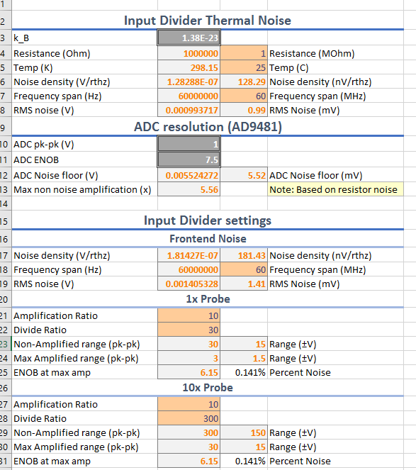
We started with our detailed design and spreadsheets:![]()
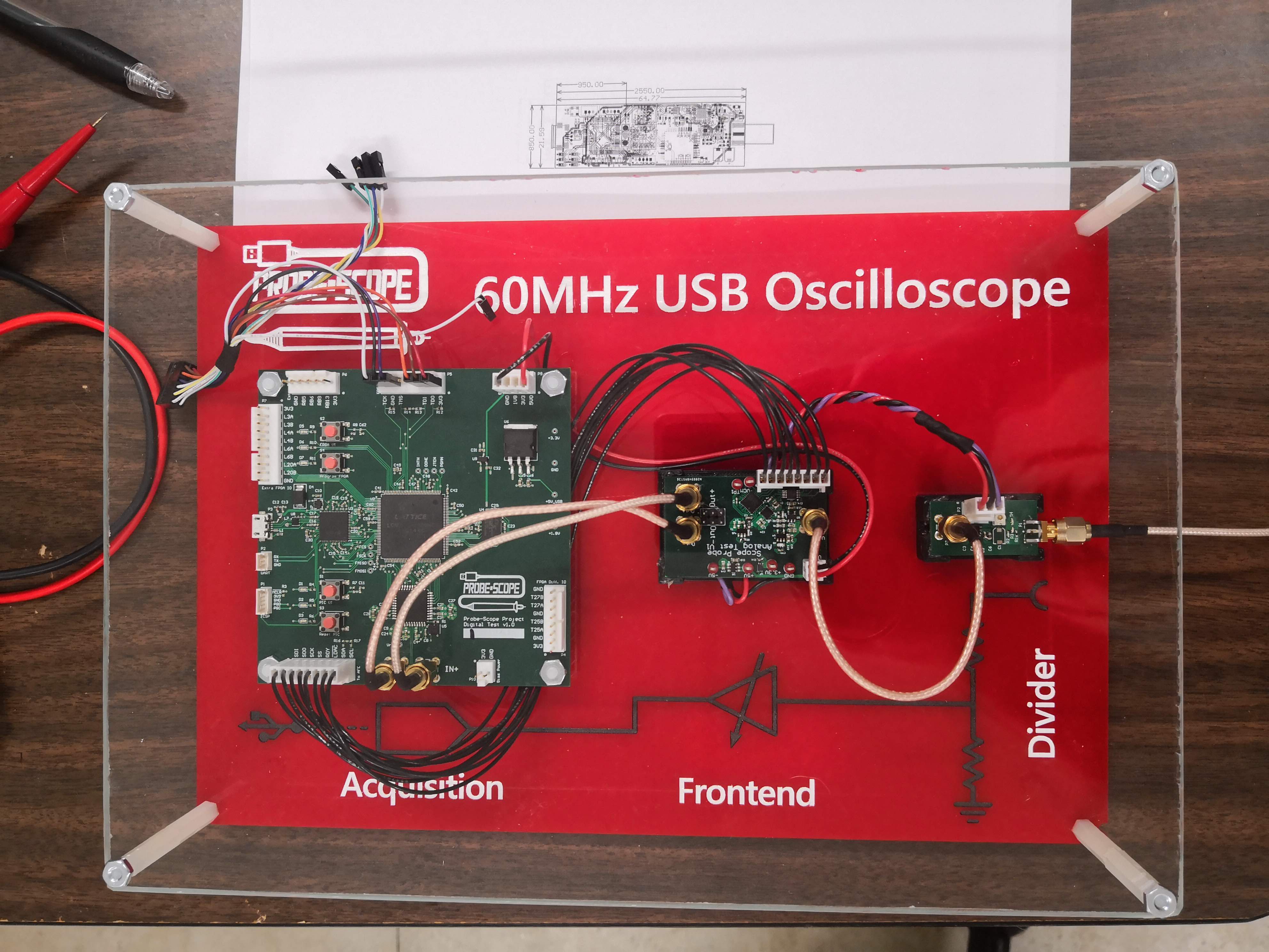
Then we moved on to a set of spread bench test PCBs to test all our subsystems:
![]()
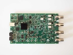
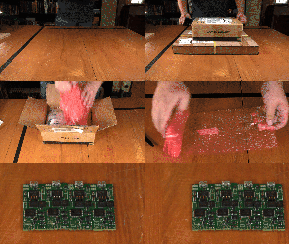
And now we have our final PCBs hot off the press from PCBWay!
![]()
Here is a guide to all our updates:
- Introduction and Overview
- Analog Frontend:
- Digital Section:
- Final Design Bring up
Here is a guide to our GitHub Repos:
- Probe-Scope V1.0 PCB
- Embedded Software:
- PC Software
- Test Boards:
- Misc:
iii. How ready is this design be taken to market?
The hardware design is complete; our final PCBs were produced and assembled by PCBWay and functioned as expected right out of the box. We are planning on using the same design for volume manufacturing, with only minor changes to the connectors. The software is coming along nicely, more details on that in our next section.
iv. How complete is the project?
We have come a long way, having completing the following portions of the project in only 5 months:
- Market research, and viability
- Predesign
- Noise, Sensitivity and Bandwidth analysis (See our original calculations)
- Pre-BOM Pricing
- Feasibility and Form Factor
- Subsystems testing and development:
- Analog Frontend:
- Designing, building and testing Frontend Divider and VGA/Filtering PCBs
- Exceeding our initial bandwidth and noise specs
- Digital Board:
- Designing, building and testing the entire digital side of the system
- Testing all the components
- Providing an easy to debug test bench for Software Development
- Analog Frontend:
- Final PCB Production:
- Designing and Producing a very complex compact PCB
- High Speed, Length Matched busses
- 0.5mm BGA
- 6 Layer
- Blind/Buried Vias
- Via in Pad
- 3/3 Trace/Space
- Reducing total board area by 88% (18.8sqin to 2.2sqin) from our development boards
- Designing and Producing a very complex compact PCB
- Embedded Software
- PIC32MZ
- Created and implemented USB CDC protocol to transfer data. (See our protocol specification)
- Implemented USB CDC, SPI, I2C
- Implemented FPGA Interface for reading samples
- MachX02 FPGA
- Implemented sampling subsystem
- Implemented sampling FIFO
- Implemented PIC32 Interface
- PIC32MZ
- PC Software
- Implemented the USB CDC protocol
- Implemented capture, scaling and display of the ADC Data
- Implemented measurements subsystem (pk-pk RMS ect…)
From here this is our software roadmap:
- Expand current FPGA sample buffering subsystem to take advantage of the full HyperRAM (giving us 16M samples of memory)
- Implement trigger sharing on FPGAs
- Implement trigger delay on the FPGA
- Implement better (More “scope like”) horizontal and vertical scrolling on the PC software
- Implement many more measurements on the PC software
- Implement trigger sharing in the PC Software
- Change to dynamic Qt widgets to allow drag and drop rearranging of the capture display
We also have some stretch goals:
- Implement support for Sigrok decoders from the PC software to gain protocol decoding support
- Implement field firmware upgrades for the PIC32MZ and the FPGA (they are already hooked up just needs software)
- More things as we get more feedback!
-
Final Boards Received
08/23/2019 at 01:31 • 0 commentsThey're here a day early!
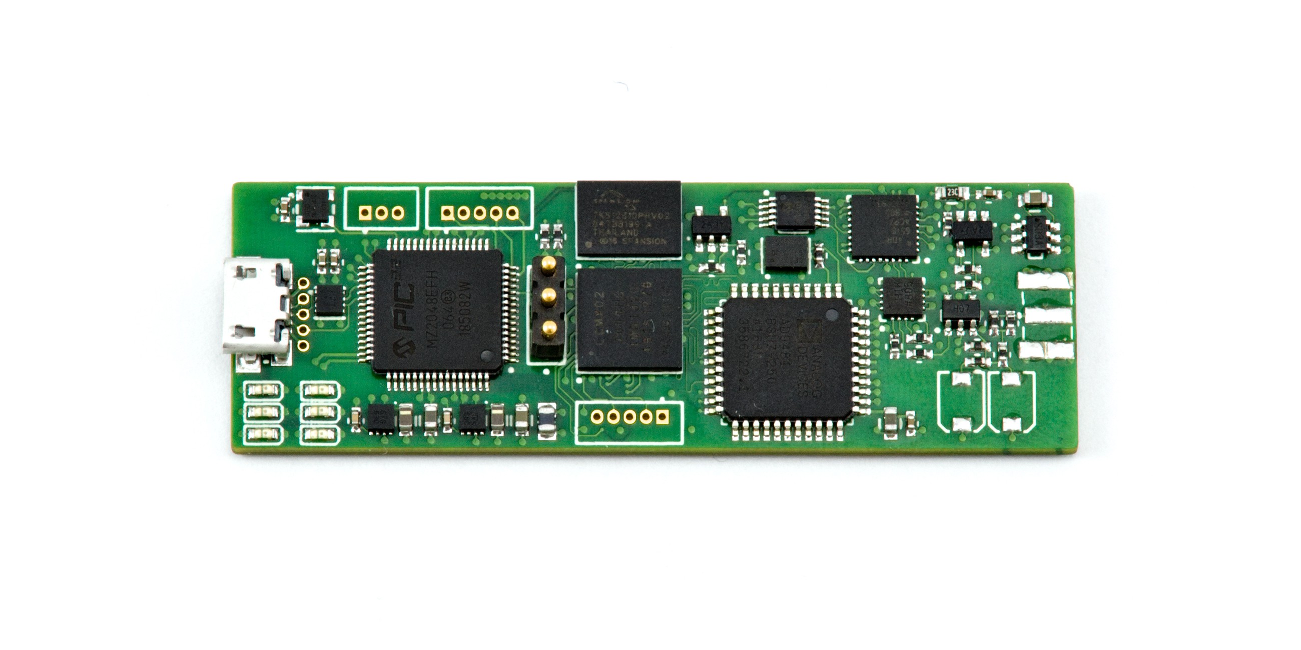
![]()
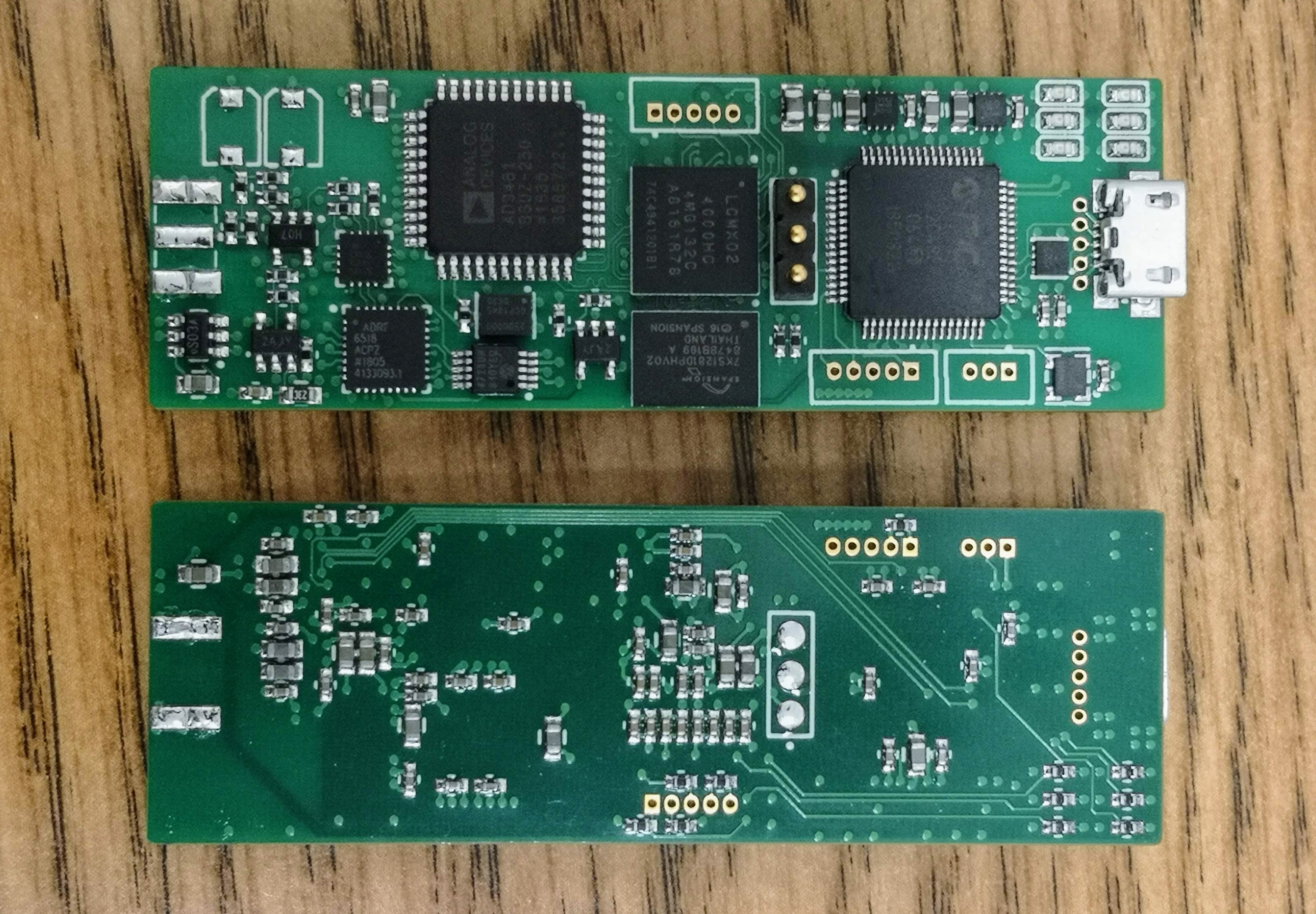
Our final boards came in this afternoon. Here's a closeup:
![]()
Kempton's making the cases for them now.
-
Acquisition Acquired
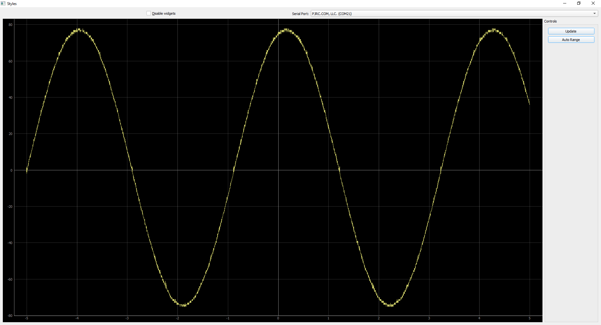
08/22/2019 at 03:58 • 0 commentsWe've squashed the bugs and straightened out the kinks... Here's the first screenshot of real data coming in from the ADC! We use pyqtgraph for the data rendering, which performs excellently and has all the plotting and UI features we want baked right in, so we've avoided sinking a ton of time into displaying the waveform. Tomorrow we will add the actual units to the GUI and support setting the parameters of the device, and on Friday we'll have the real boards in our hands.
(disclaimer: we're driving the ADC directly with a function generator here, just for simplicity's sake)
(also disclaimer: we're not using a teensy and I don't know why Windows thinks it is one, only on this computer does it say that...)
-
Software and Stuff
08/20/2019 at 22:33 • 0 commentsAs we mentioned a few weeks ago, we had hoped to post an update about the software by now. So where's it at? We haven't shared anything yet because we have a lot of moving pieces in this system (FPGA acquisition, FIFO, and sample output, PIC sample ingress, PIC USB comms and protocol, host comms and protocol, host GUI, and host measurement features), many of which are working quite well in and of themselves, but the product as a whole isn't quite ready to roll. We will be finishing it this week of course, and we're confident we will have something impressive to show off by Saturday.
We haven't been doing nothing, however: Aside from continually working on the software, we put together a demonstration unit and showed it off at the Microchip MASTERs conference about two weeks ago, along with a very early version of the software. Check it out:
![]()
And while it's not really relevant to what we're doing now, here's a neat short video I put together a while ago of us assembling the digital test board:
Finally, we just got word (and pictures!) from our PCBA vendor that our final boards have been assembled, so we'll get those in the next two or three days, just in time to show them off to you all in our final submission. Stay tuned!
-
Final Probe Scope PCB
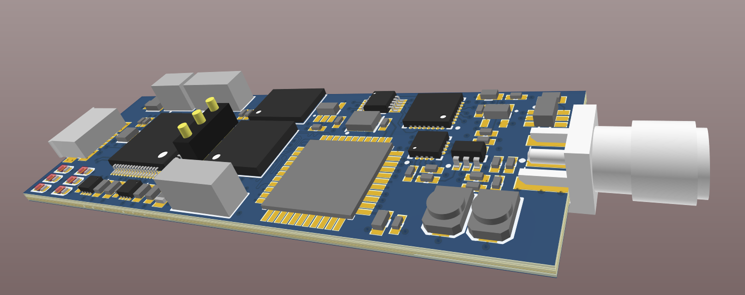
07/28/2019 at 17:40 • 0 commentsWe recently finished the layout of our final probe scope available on our github, now an obligatory PCB picture:
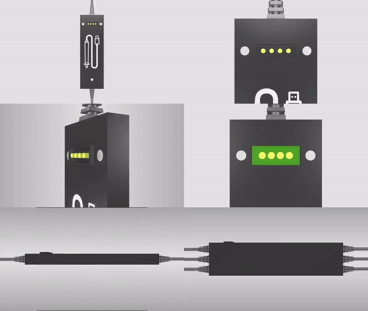
Here is an animation of how the Probe Scope stacks, to allow expanding to multiple channels all connected to one PC. The contacts on every Probe Scope distribute the trigger signal from the master Probe Scope to all the slave devices for synchronization.
![]()
We sent away the PCBs to our favorite PCB vender, PCBWay for assemble and fabrication.
In other news, we are working hard on the Digital Test Board, developing all the software. We hope to post an update at the beginning of next week.
-
Digital Test Board – Built Up, Lights Up
07/13/2019 at 05:01 • 0 commentsWe recently got our PCBs in and built up, and having detailed the testing of the analog boards, it’s time to show off the Digital Test Board in its early stages. Unlike the analog boards, where the bulk of the work was done in designing them before they were made, this was straightforward to design and will take much more effort to program. So, expect some more updates over the weeks as all the software and firmware gets put together.
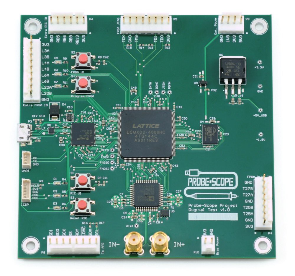
First, a glamour shot:
![]()
We need to get the final Probe-Scope board designed and sent out fairly soon, since the lead times for getting it made and assembled (and we will be getting it assembled) are pretty long due to the high density, and the competition deadline is approaching. So, to start off, we’re just verifying that all the pieces of the digital test board work so that we can be comfortable reusing those schematics in the final design. That means probing the ADC to make sure it’s outputting data (it is), loading code onto the PIC and FPGA to make sure they run with the correct clock sources, and then eventually (not done yet but soon) implementing a simple USB device on the PIC, and operating the HyperRAM with the FPGA.
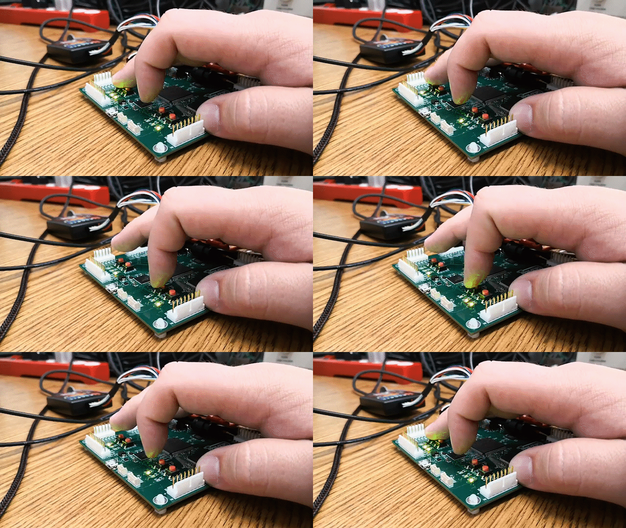
The PIC was easy to get running as we have some lightweight test code we often reuse, and it works just fine with the external 24MHz oscillator (which is basically required for USB to work). The FPGA, on the other hand, was a bit more of a challenge for me as I have not used Lattice Diamond before, and its documentation is very spread out. Pro-tip: the file list has tabs at the bottom… you really want to check out the process tab. At any rate, I got that running too, clocked off the output of the ADC. Watch it all blink:
![]()
This leaves the USB and the RAM to be tested. The USB connections and clock, I’m not too worried about, they match known good designs. The RAM however, I’m also not too worried about, but it remains to be proven that our concept of clocking it at a higher speed using the FPGA’s PLL will work in this exact configuration. Stay tuned…
EDIT: The PLL for the RAM worked perfectly fine, thanks to the configurator it wasn't a pain at all.
-
Assembly and Analysis of the Analog Frontend with VGA
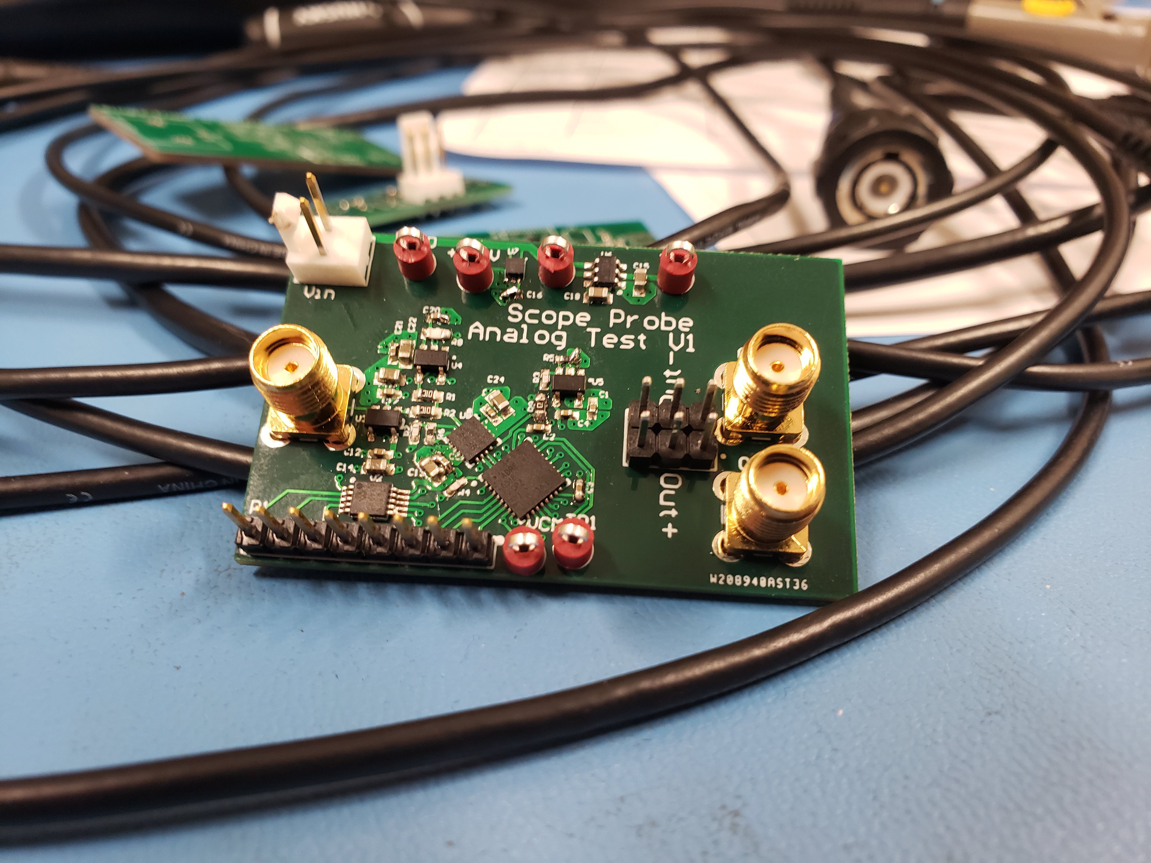
07/10/2019 at 14:58 • 0 commentsHaving recently received the parts and PCBs for all of our subsystem test boards, this post is one in a series detailing the buildup and testing of those boards. Today we’ll be showing off our Analog Frontend board, which includes the Variable Gain Amplifier (VGA) and Filter that makes the whole thing work. To start, here’s a picture of the finished board
![]()
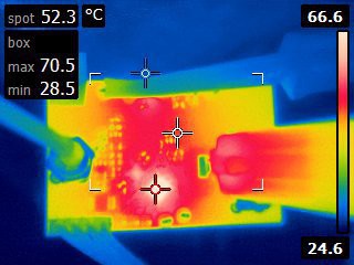
After cursing the designer of the board (me), who decided that 0402 was the right size for most of the components, I finally got it assembled and up and running. One of the first things that I noticed was that it ran hot. In the back of my mind, I knew that the VGA (an ADRF6518) drew a lot of power (400mA at 3.3V or around 1.3W), but I didn’t quite consider the thermal implications of that. Checking the board with a thermal camera (shown below), the VGA got all the way up to around 70°C, which is actually right about the calculated value, but of course, I forgot to calculate it beforehand…
![]()
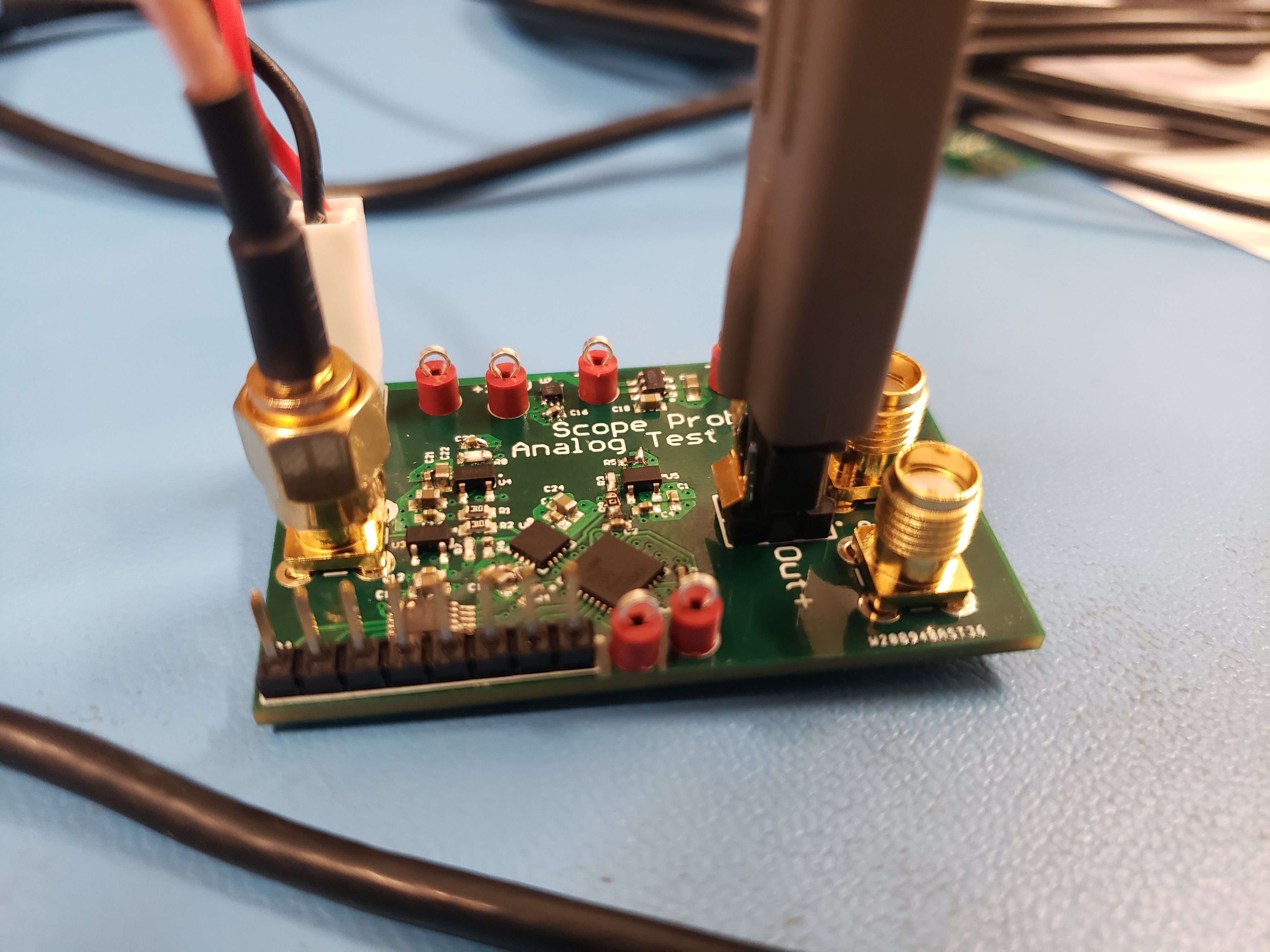
The first thing I did was write some Python scripts for my Raspberry Pi to control the ADRF6518 (over SPI), letting me play with its bandwidth and gain settings, along with controlling the MCP4728 DAC that set the Offset and Gain levels. Once I got it all set up and working, I connected it to our DG8SAQ VNA in order to get some frequency response plots, and they looked amazing! Here’s a picture of the board all hooked up for testing. I’m using a Tek P6248 differential probe (plugged in on the right) to feed the signal into the DG8SAQ.
![]()
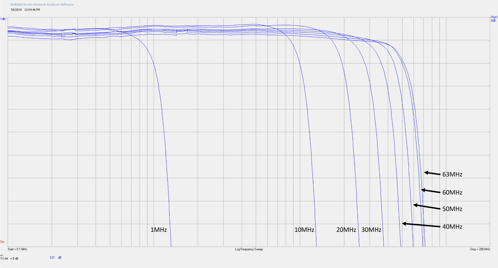
Shown below is a screenshot of the results, with five sweeps at five different bandwidth settings, from 1MHz to 63MHz (the maximum setting).
![]()
As you can see, the gain is flatter than 0.5dB overall, and for individual settings it’s better than 0.1dB. And now here’s a screenshot zoomed all the way out, with the bandwidth set at 50MHz. To achieve an ENOB of 8 bits, we need at least 50dB of rejection at our Nyquist frequency (125MHz) in order to prevent aliasing. Here we get 80dB of rejection, well beyond the requirement.
![]()
The frontend was working so well, in fact, that I decided to test it at 63MHz (the maximum frequency of our VGA Filter) and we were able to get 65dB of rejection! Therefore, we can comfortably rate the Probe-Scope’s maximum bandwidth as 63MHz, surpassing our design goal of 50MHz.
You can find the schematics and layout for this board on our GitHub, or if you go back to an older project log, there’s a screenshot of it too. Next on the list is the Digital Test Board, which we’ll have a short post about just verifying its hardware up soon.
-
Assembly and Testing of the Frontend Divider!
07/09/2019 at 05:16 • 0 commentsWe just got in the parts and PCBs for all our test boards, so this will be the first of several posts on the testing and bring up of the boards.
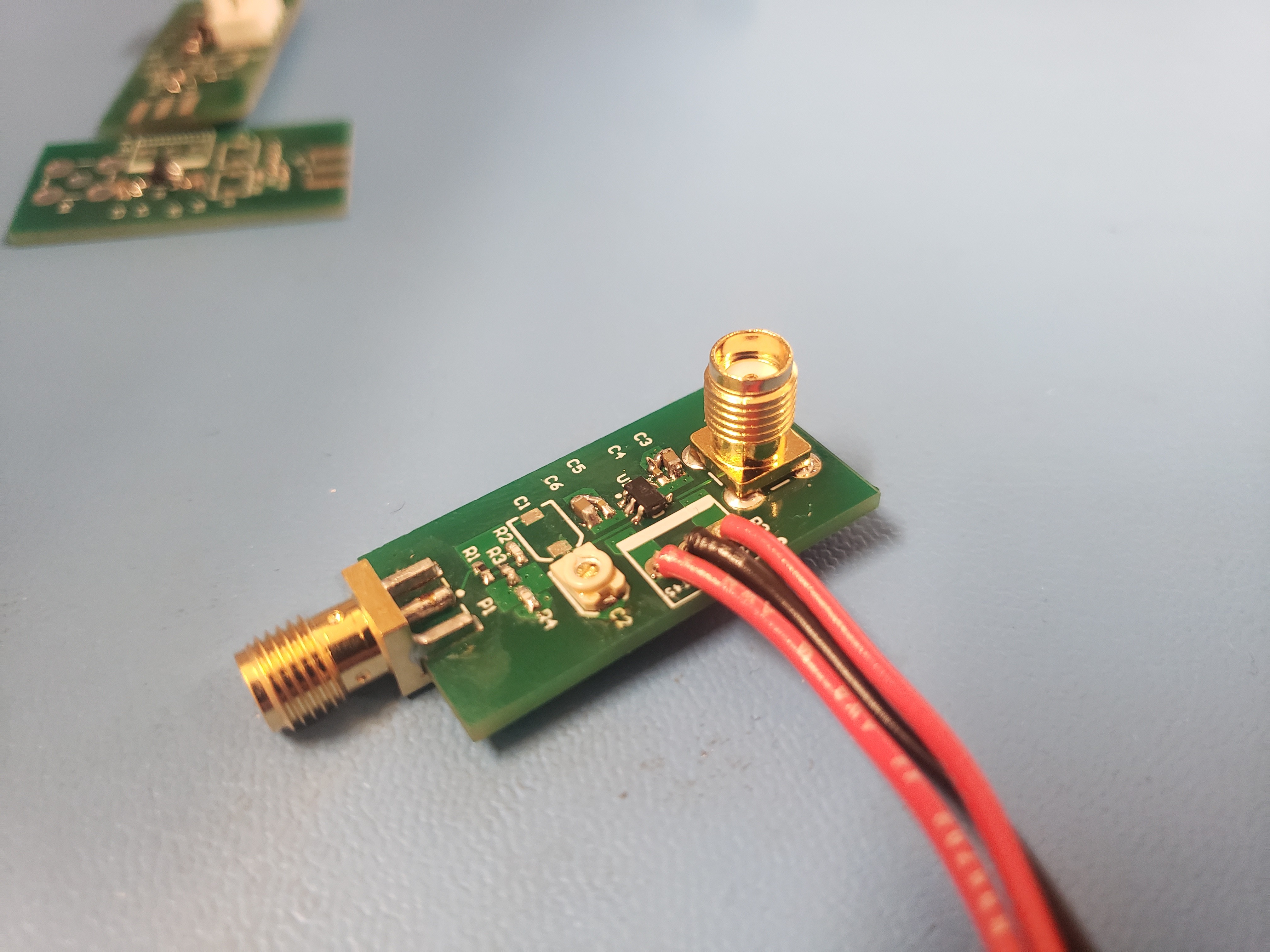
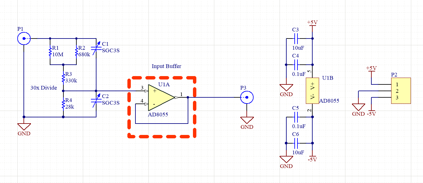
The first board we built and tested is the Frontend Divider test board (for a detailed explanation of why this board is so complex and needs careful attention, see our previous post). Below is the assembled Frontend Divider board. It contains a 30x resistor divider with special layout considerations, a tuning capacitor to ensure a flat response, and the frontend buffer amplifier.
![]()
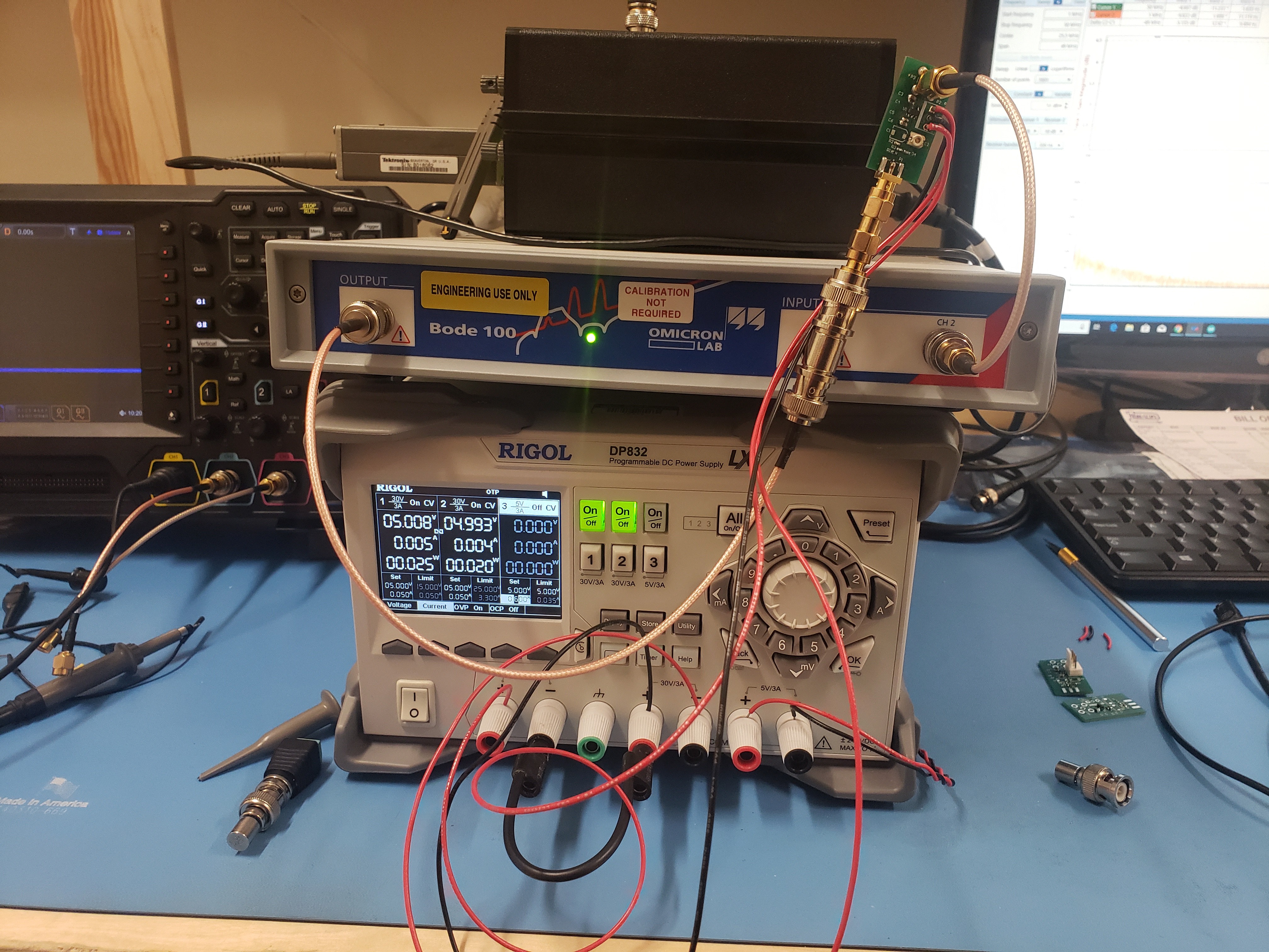
Ideally, we’ll be able to tune the divider so that the frequency response is very flat; in order to test that, I connected it up to our Bode 100 Vector Network Analyzer, a low-cost, (relatively) low bandwidth USB VNA. It can perform several measurements over a range of frequencies (from 1Hz to 50MHz), most importantly for us, it can measure Gain Magnitude, Gain Phase and Group Delay.
Here is a picture of the Frontend Divider board hooked up to the Bode 100… do ignore the mess.
![]()
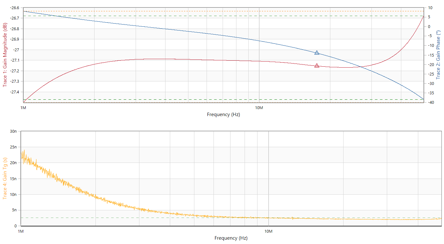
After a bit of fiddling with the tuning capacitor’s value, I was greeted by this beautiful bode plot:
The gain is almost perfectly flat across the board, and while the constantly decreasing phase might instill some concern at first, that too is our desired outcome. (It’s what we want in order to get a constant group delay, which we’ll cover in detail in a future article.)
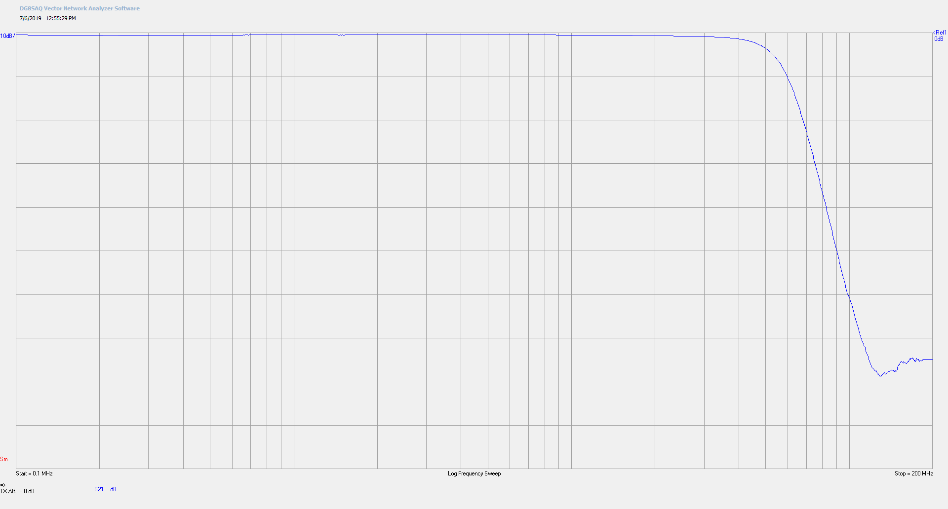
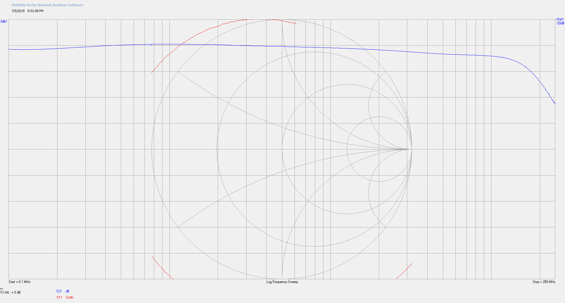
Here’s some more detailed plots of the Gain, Phase and Group Delay (shown as Gain Tg):Now, in order to measure past 50MHz and fully understand the performance of our Frontend Divider, we need to switch to another instrument: the DG8SAQ VNA from SDR-Kits. The DG8SAQ is a low-cost VNA which can measure from 1kHz to 1.3GHz. I swept our fronted from 100kHz to 250MHz. You can see from the plots below that the Frontend Divider is not the bottleneck of the Probe-Scope; it actually has a bandwidth of more than 150MHZ!
![]()
For the curious readers, the Frontend Divider schematic is shown below, and as with everything we do, the source can be found on our Github.
![]()
60MHz Bandwidth 250Msps Probe-Scope
The Probe-Scope is an open source 60MHz 250Msps oscilloscope probe with all guts built right in, that plugs directly into your PC via USB
 Mark Omo

