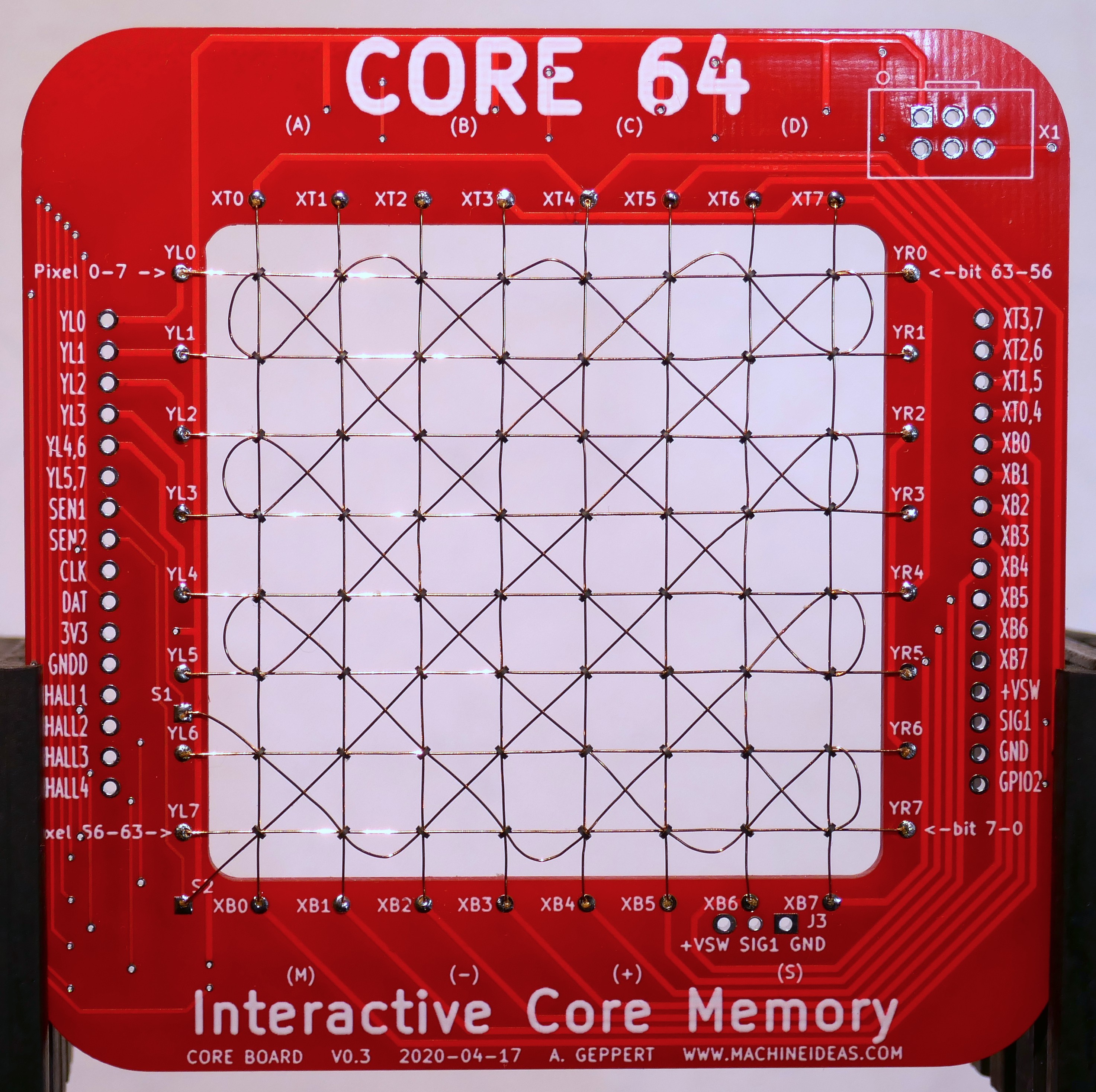
Despite a lack of log updates, I have been making a lot of progress toward the next round of prototypes. I have moved to a dual board design which presents the core array on its own circuit board. The decision incurred a lot of work in creating two new PCBs with proper interconnections. Regardless, I'm happy with the results so far. This time the core weaving went much faster, and the results are more consistent.

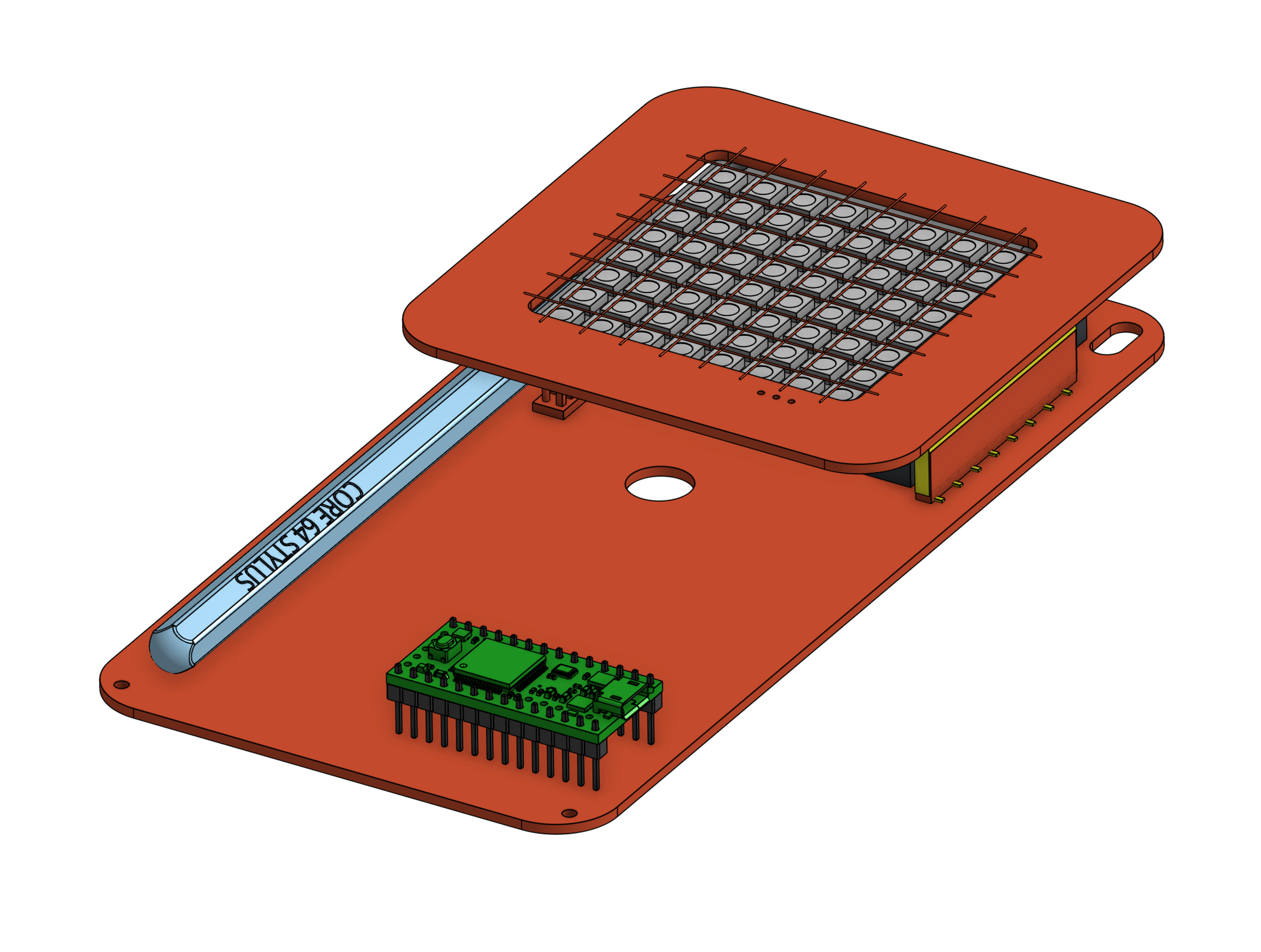
The second board is twice as tall, and will support all of the logic functions. The core board will plug into the top of the logic board, like this:

I'm looking forward to receiving the logic board in the next 3 days. In the meantime, I aim to complete the assembly of the core board and complete some basic tests.
The benefits of this revised approach are:
- A more physically robust design that does not require a supporting enclosure on the back side. It also sits flat/stable on a table surface.
- All of the components on the logic board are on the top which makes troubleshooting much easier.
- The core board can be sold separately with a much lower cost so potential buyers can make a minimal investment to see if they want to follow through with the complete project before committing to the more expensive logic board.
- It is easier to assemble the smaller core board on its own.
- The sandwiched design hides the battery pack between the boards, and provides an area to secure the stylus (with 3D printed balogna between the boards).
Here's to prompt shipping by FEDEX for the Digi-Key.com components, and to DHL for the logic boards from JLCPCB.com. It'd be great to receive them this weekend, please!
 Andy Geppert
Discussions
Become a Hackaday.io Member
Create an account to leave a comment. Already have an account? Log In.