-
Schematic
07/12/2019 at 01:57 • 22 commentsSchematic
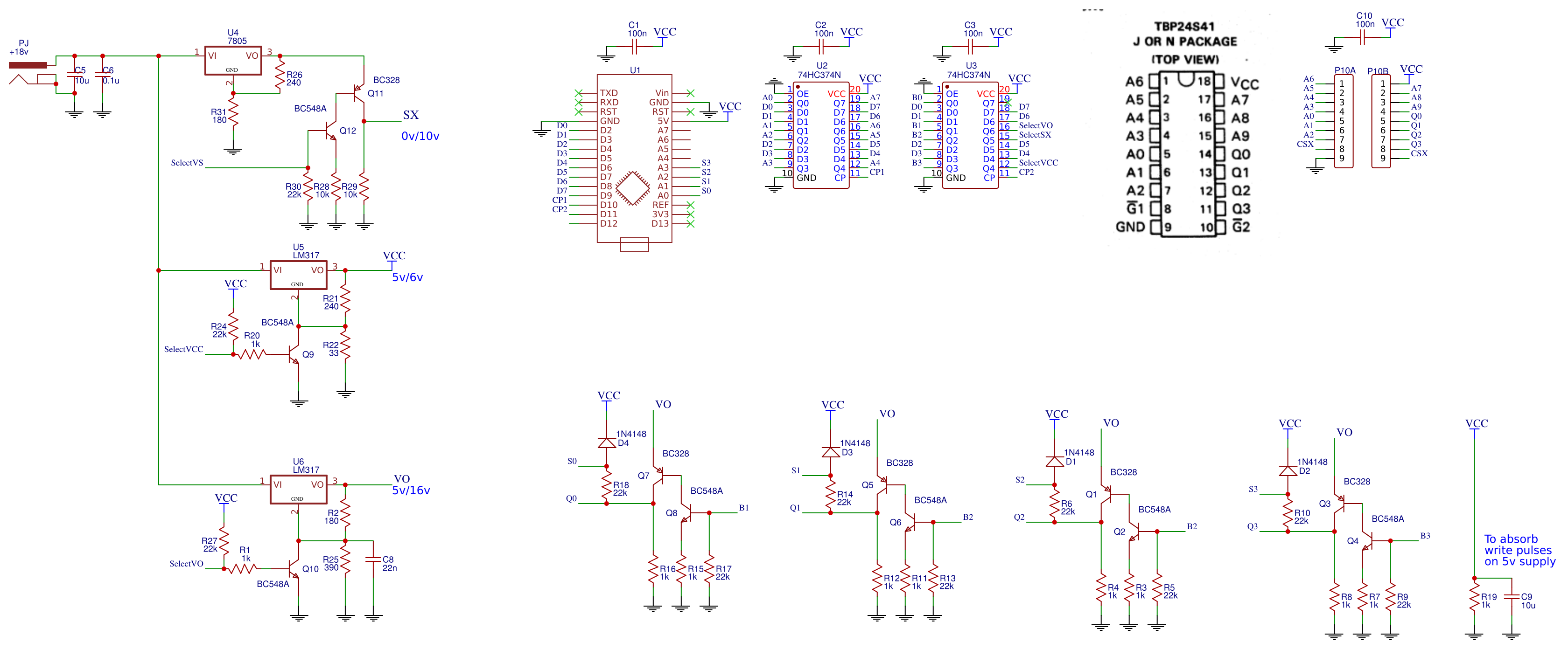
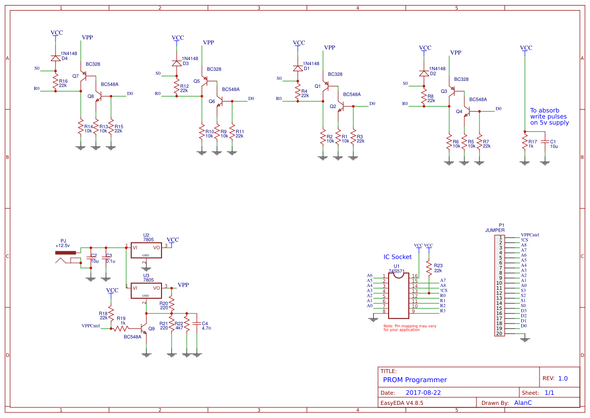
I knocked up a schematic for the programmer:
![]()
And I tested the component values (for the 16v pulse):
![]()
The voltage/current is pushing it for the BC328 so it may be necessary to check output voltage before using the programmer in "anger".
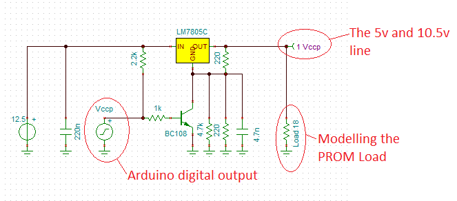
Here is the schematic that I simulated:
I probably should add a pull down resistor on the base of T1 BC547.
Without the "bit" switch the output from the regulator would look like:
![]()
Best to let the dust settle on the design before I do a last check and knock up the PCB.
Updates
The minimum input voltage is 18.5v rather than 18v, and R2 should be increased from 180R to 200R.
Also worked out how to pull VCC to ground if it is a desired feature of the programmer.
I also "spat the dummy" with EasyEDA and have migrated to KiCAD.
Nearly as bad! How can you have a recommended install with no libraries.
It is a real headache for a novice to workout what libraries are required, where to put them, and how to link them in.
I will get there but why make it so *%#$^!? hard!
Need
I don't actually have a need for this programmer so I will not be designing the PCB.
And Danny is keen to go the prototype path rather than the PCB path.
AlanX
-
The 24S41 Datasheet
07/11/2019 at 09:21 • 0 commentsIn the beginning
I have built a programmer for the74S471 PROM for my https://hackaday.io/project/12879-weird-cpu project. And I contributed to Yann Guidon's https://hackaday.io/project/25953-promer project.
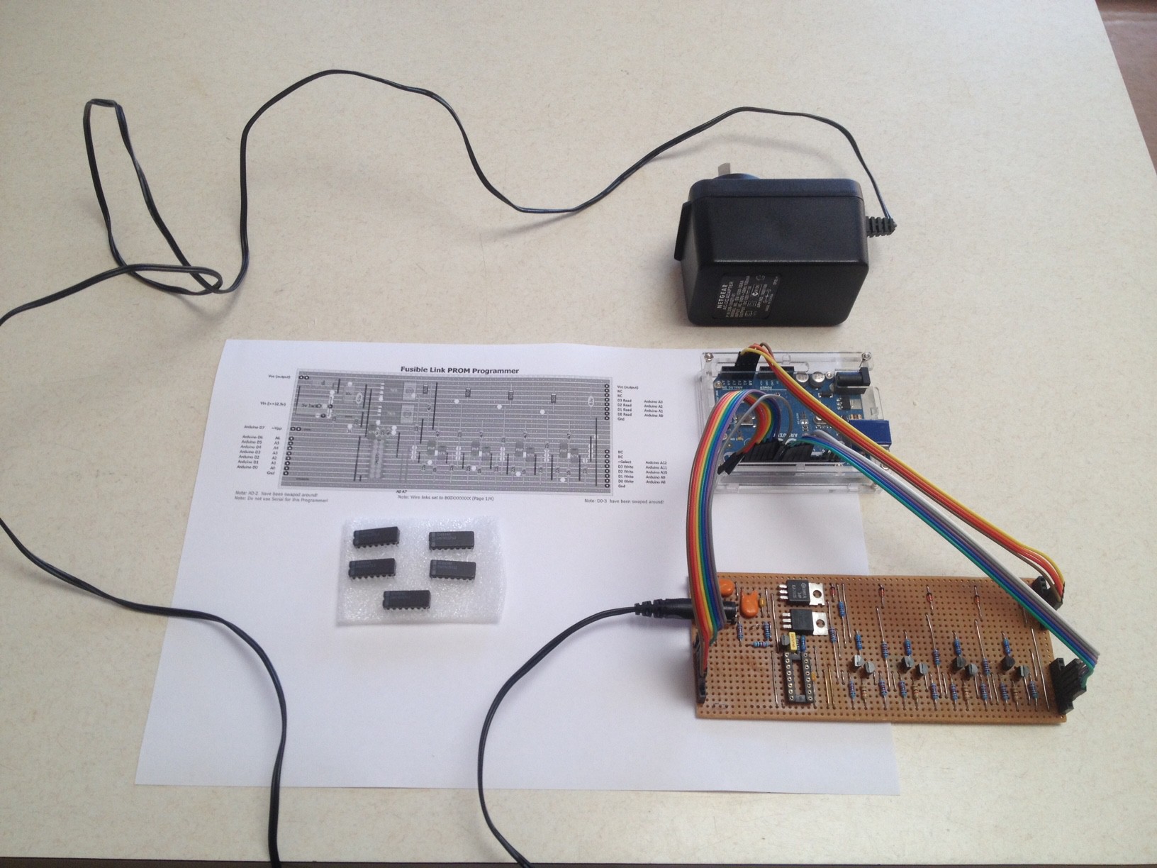
Here is my 74S471 PROM programmer:
So how hard could it be to design on fro the 24S41?
The process starts with finding and downloading the data-sheet:
https://www.ti.com/lit/ds/symlink/jbp28s42.pdf
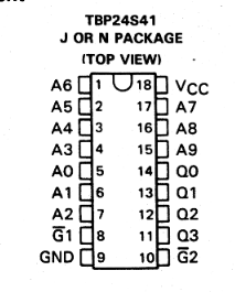
Okay, that was not hard. Here is the pin out in which I will need for the PCB design:
![]()
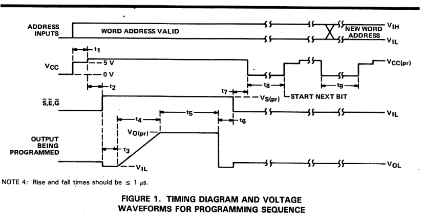
Okay, here is the timing diagram:
![]()
Not nice! Three (or is it four) programming voltages (5v/6v, 10v and 16v) that pull down to zero volts. Pulling down to zero is more difficult than just pulling down to 5v. The 74S573 by comparison only needs only 5v and a 5v to 10.5v programming pulse.
Oh well, Danny has already bought his chips.
An additional difficulty is that the higher voltages. If using a shunt regulator then they will need sizable heat sinks. But using switching mode regulators just adds another level of complexity to the project. So I will stay with shunt regulators. They are simple to use and good enough for this project (even with big heat sinks).
What is going on in the timing diagram?
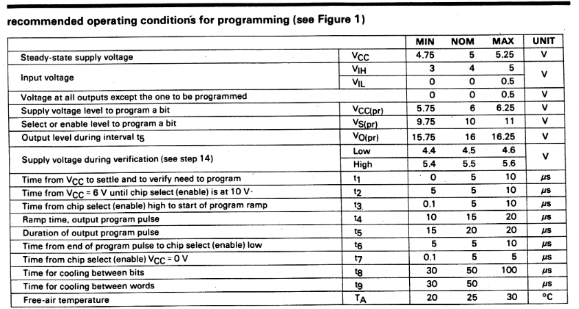
Here are the voltage and timing specifications:
![]()
Okay, there are quite a few good hints here to what is going on: t8 and t9 are required to cool down the chip. t1 is optional.
Heat Dissipation Management
The 74S471 recommends a maximum programming cycle duty of 24% for heat dissipation management. In the 24S41 case they add power off periods (i.e. t8 and t9) during the programming cycle to manage heat dissipation. I really want to get rid of t8 and t9 as they require pulling the supply voltage (Vcc) down to zero.
So instead I will extend t1 to double of the average of t8 and t9, or about 100us (absolute minimum). Now the design is much simpler.
Voltage Control
With my 74S471 PROM programmer I used shunt regulators because they are very simple to design. The only down side is that they can get quite hot without a suitable heat sink.
So here is my 74S471 design:
![]()
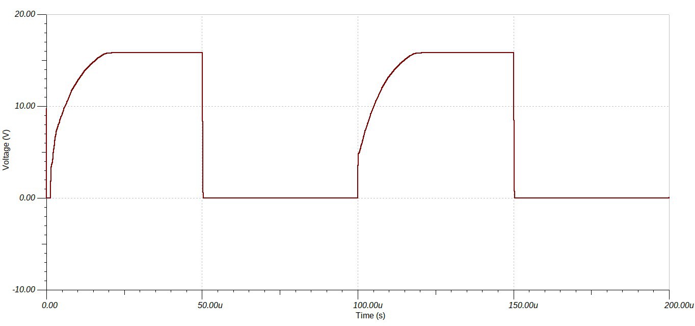
Lets start with the voltage regulators. Here is my circuit simulation schematic:
![]()
And the simulation results:
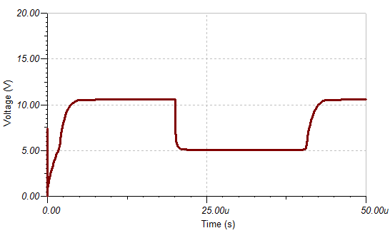
![]()
The result is not a perfect straight line ramp up as suggested by the timing diagram but good enough. The ramp up for the 74S741 should be between 1 and 10 us. For the 24S41 it needs to be between 10 and 20 us seconds, so I will have to slow the ramp up for Danny's design.
I think I will have to use the LM317 voltage regulator. This can be adjusted from 1.2v (not 0v) and up to 37v. I have some ideas I need to explore here. I think I can get away with 1.2 volts (the minimum for the LM317) rather than 0 volts.The other voltage regulators do not have ramp up requirements.
Bit Switches
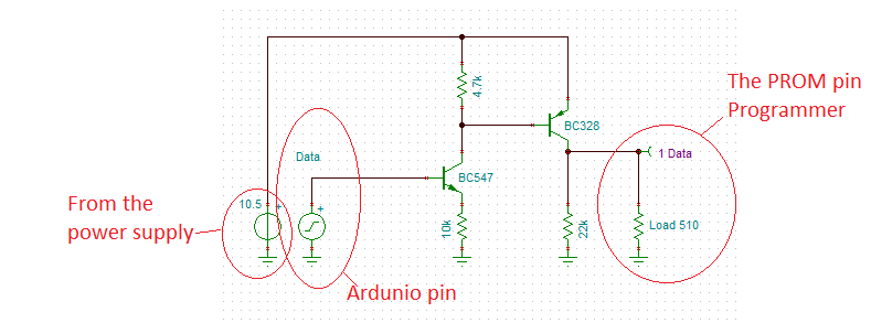
When you program the PROM you can only program one bit at a time so an electronic switch is required. I use a two transistor design worked well for my 74S471 PROM programmer design:
![]()
It is a pretty simple transistor switch. The BC547 buffers the input and the BC328 pulls the output voltage up to within 0.1 or 0.2 volts of the supply voltage. When off, the 22k resistor pull the output voltage down to near 0 volts.
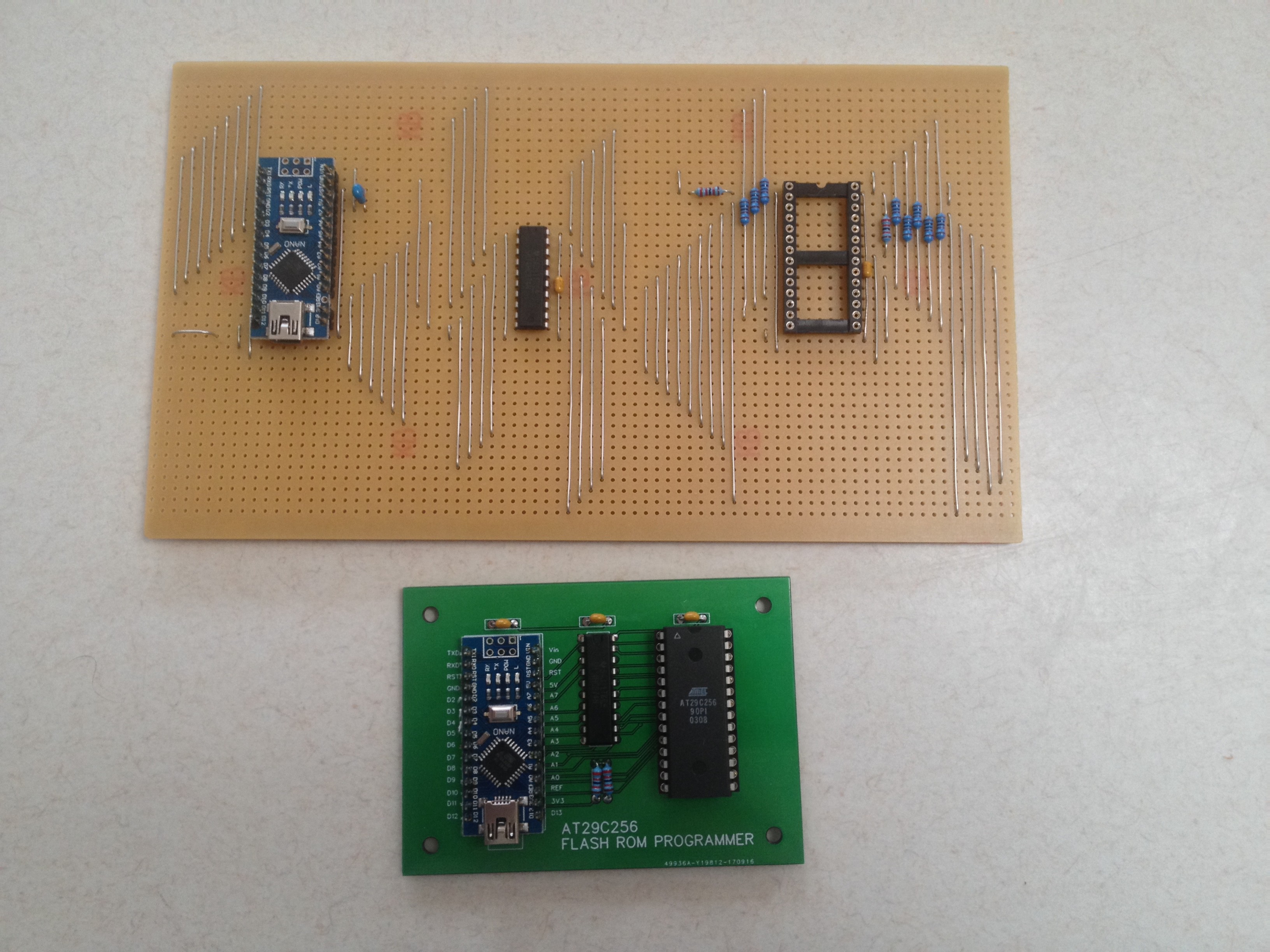
The final design "box" is the Arduino Nano. In the past I just plugged in a share Arduino. The problem is that every time I do this I have to reacquaint myself with the hook up procedure. Better to build it in. Here are two example for my AT29C256 FRAM programmer:
What is that chip in the middle? The Nano does not have enough GPIOs, so the middle chip (a 74HC374) latches the FRAM upper address space. I will have to do something similar for this programmer as well.
What Remains?
Well most of the hardware has been covered, what remains is the software. Now Danny is a software engineer so I am going to leave that to him to sort out. I am interested in what he come up with!
And finally I will knock up a PCB design.
Update
I was checking the LM317 spice model and it seems that the rise time is in the order of 250 usec. So it is completely unsuitable for this application. Nothing mentioned in the datasheet.
AlanX
Designing a PROM Programmer for the 24S41
Danny approached me to help with building a programmer some 24S41 PROM chips for an Apple III restoration project.
 agp.cooper