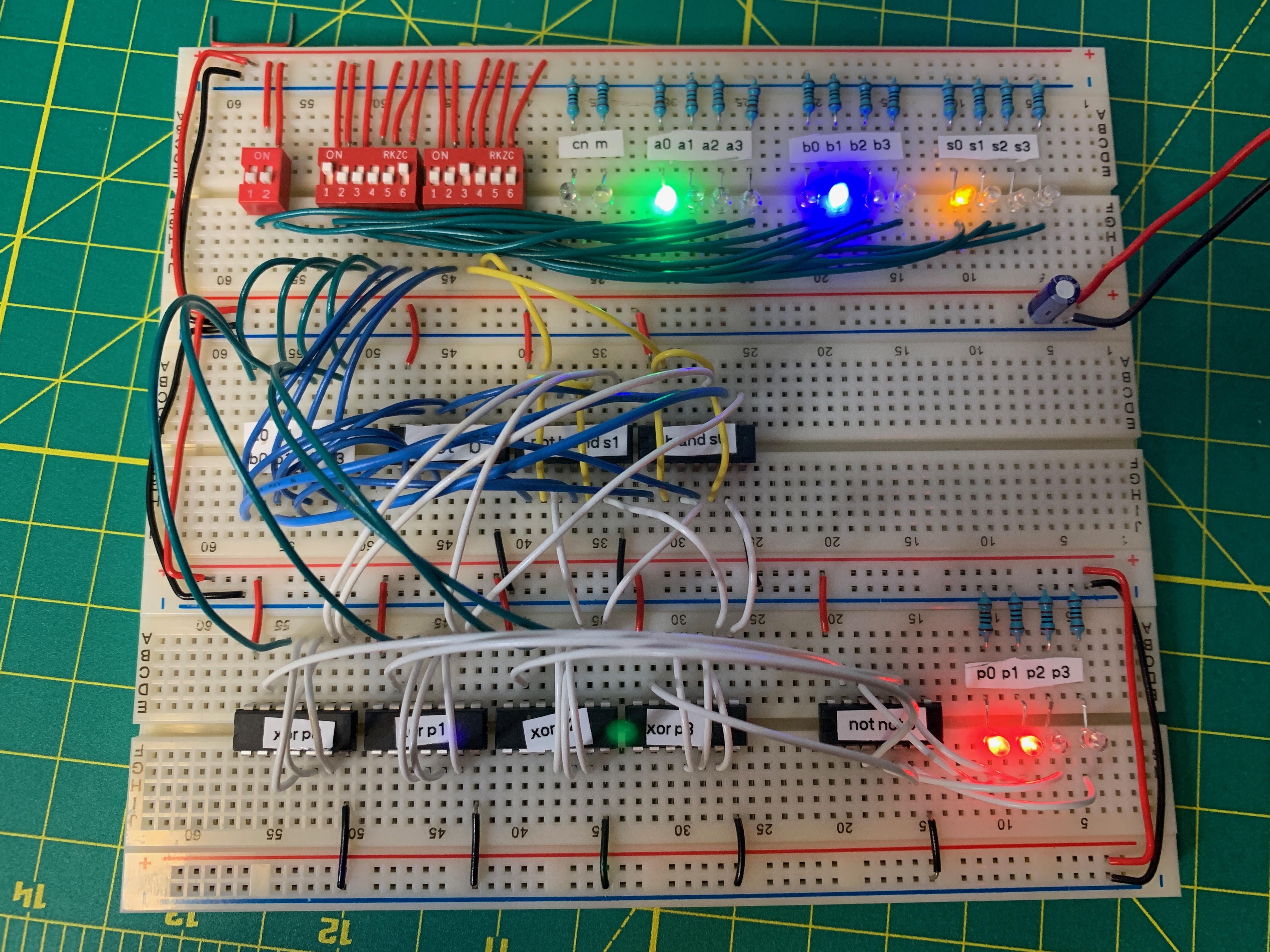
Two days ago I completed the propagator P output for the model 74181. It looked like a complete mess.

The circuit was functional, but didn't really serve the purpose of making that functionality transparent. I mean, there's a laundry list of bad things going on here.
- The wiring is crazy.
- The breadboards are upside down. WTF.
- I labeled the nor gates as xor gates. Not sure how I managed that.
- I'm using chained nor gates instead of chained or gates and an inverter. This is just me thinking too literally in my excitement to get started.
This didn't meet my standard. I ripped everything out and reworked the circuit.
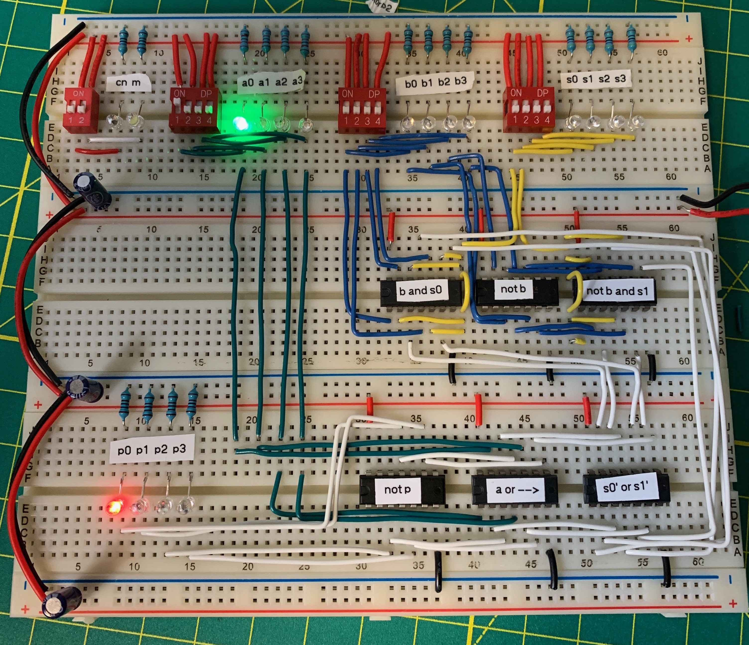
Here is the current state of the model:

The input switches are more clearly separated. These DIPS do not want to stay in the breadboard, though, so I ordered a different kind to see if I can get better results.
The organization of the logic is as follows:
- Wires & LEDs are color coded. A is green, B is blue, S is yellow.
- The first board represents the inputs to the ALU.
- The second board inverts B (not b) and handles the combinations of (b and s0) and (not b and s1).
- The third board is read from right to left. The chip (s0' or s1') is the logical OR of the second board's AND gates. The chip (a or -->) is the logical OR of the A inputs and the results of the first OR. These two ORs produce the propagate bits. The chip not p inverts the propagate bits, as the rest of the circuit will use not p instead of p.
- The intermediate p indicator LEDs show you propagate bits for each position.
I'm pretty happy with the progress so far and I've now hooked up this logic enough times that I understand it well.
The next task will be to wire up the generate bits!
 Brandon Reinhart
Discussions
Become a Hackaday.io Member
Create an account to leave a comment. Already have an account? Log In.
fantastic looking build!
Are you sure? yes | no
Thanks!
Are you sure? yes | no