Today I had a large chunk of uninterrupted time to work on this project and a bunch of progress resulted.
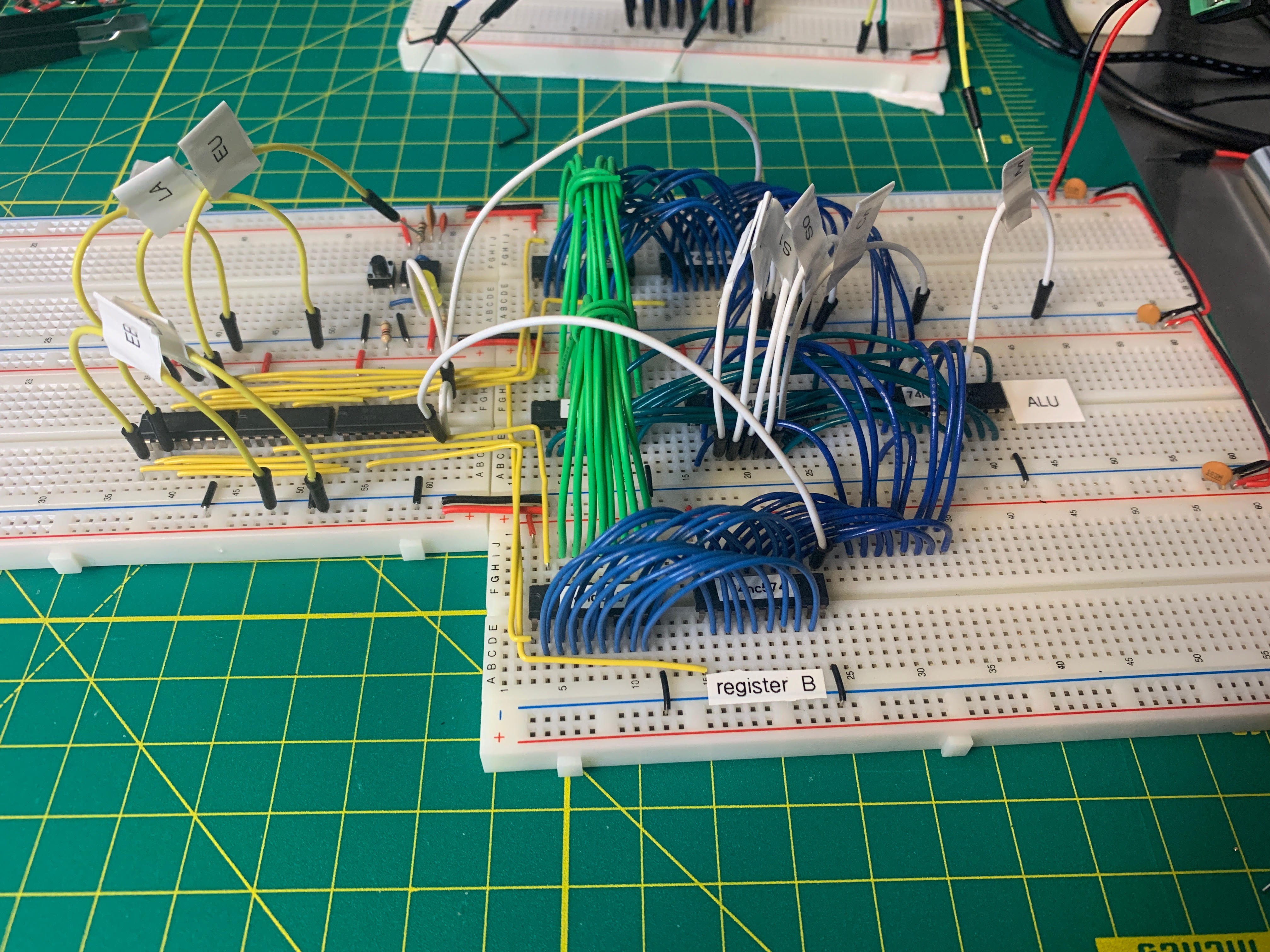
First, I wired up a pair of 74HC181s, 4-bit arithmetic logic unit and function generators. I didn't run through an exhaustive set of tests, but I did ensure that several operations worked correctly. I'm generally confident the wiring is good. Here you can see the ALU with various control lines labeled.

I also spent some time hooking up the control logic for the A and B registers. Each of these registers has an E and L control for enable-output and load, respectively. When Ex is high, the register should export its value to the bus. When Lx is high, the register should clock in a new value at the next rising clock edge. If both are low, the register should be in a high-impedance state.
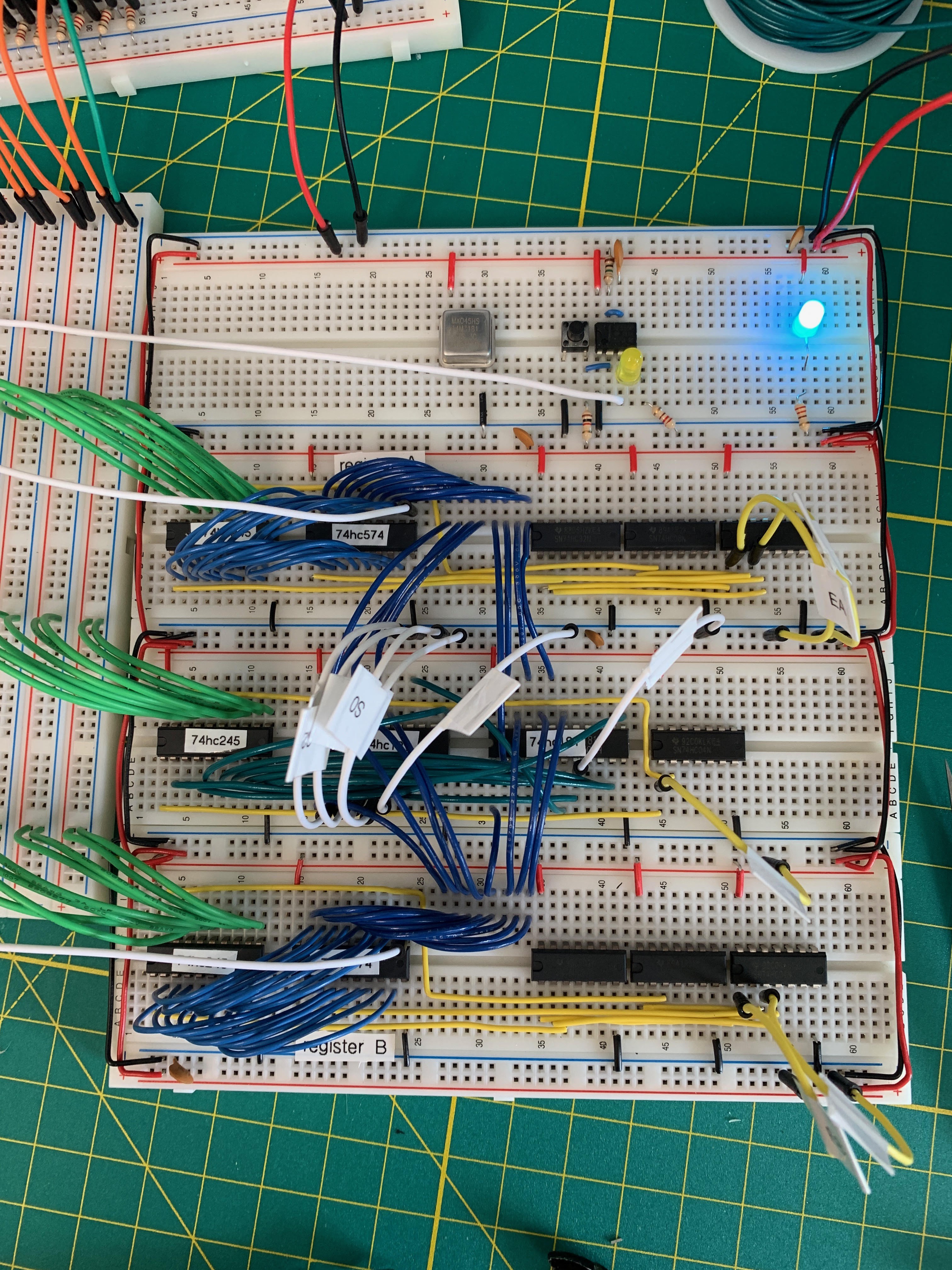
My first pass at this logic was inefficient, using a chip array for each register. This is the right half the board (yellow wiring) in the image below.

After getting this working, I sat back to think about the geometry of the computer. I didn't like the inefficient use of the chips, I didn't like how the lines ran the entire length of the board to the bus transceiver on the left, and I also wanted to change how I was doing the central data bus.
Originally, I was thinking that the data bus would run down the middle of the machine, like in the Ben Eater computer. Here's my finished version of what that kind of design looks like:

I don't like how the control bus is a crow's nest of yellow wires. So, for this computer, I think I'll try a wider design that puts the CON logic in the center of the computer.
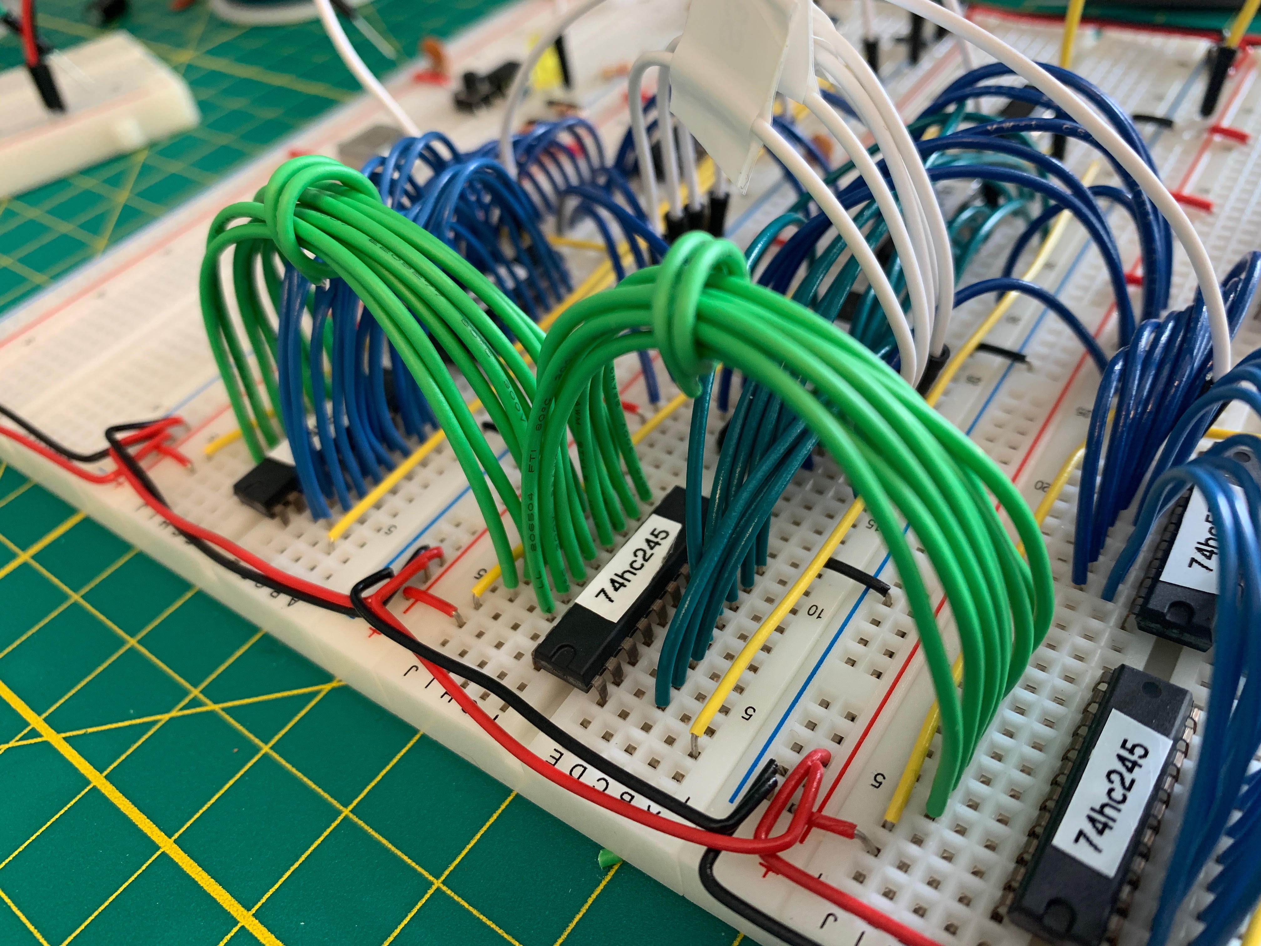
After an hour of re-organizational wiring and listening to Conversations with Tyler, I ended up with a much cleaner set of control logic for the registers and the ALU, although I haven't relocated the S, Cn, and M leads yet:

You can see how the green data bus lines are now daisy chained along the transceivers. The clock stepping switch that I use for testing is now also located in this central area. The white clock leads are temporary. In fact, that entire CON block will probably get refactored a couple times as more pieces come into place. I haven't worked out the layout on paper and I may do that soon.
Here is a look at the complete computer so far:

The left side of the board has the program counter, the incomplete subroutine counter, and a 64K ram chip roughly where the memory will be. The center is the new CON block and the right are the registers A and B and the ALU.
I think at this point the left side needs some attention. I need to make some progress on the address bus, although I also need to complete the subroutine counter and the index register. Once all of that is done, I'll have to work on the instruction register and the instruction decoder. I figure the control logic will develop stepwise with the various modules.
I've also been thinking about input, output, and how to program the computer. I'd rather not program this machine with DIP switches. I'm leaning towards hooking up a bootstrap loader that can dump code into the RAM on startup. That would be removable, allowing me to code the computer with an assembler on the PC. For output, maybe some kind of LED array? The problem with a lot of those devices is that they require a very high refresh rate, some > 500 Mhz, which this device won't be able to deliver.
Onwards!

 Brandon Reinhart
Discussions
Become a Hackaday.io Member
Create an account to leave a comment. Already have an account? Log In.
I also added an oscillating rainbow LED that I had leftover from a hackerbox as a PWR indicator.
Are you sure? yes | no