 Mike Teachman
The Mission
I needed some stripboard for a prototype. Even in the age of Oshpark and JLCPCB I still find stripboard prototypes to be useful. I can make them in an afternoon and they are easy to modify.
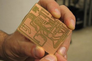
But, where to source stripboard? Veroboard is really expensive. Ebay stripboard is really low quality - holes are drilled off center, boards are warped, and rework lifts the pads. Adafruit Perma-Proto is excellent, but only comes in the breadboard form factors.
Then, came my insight (albeit a really small insight)...
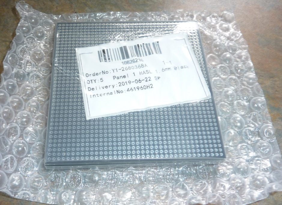
I can get a low-cost PCB supplier to make pretty decent stripboard. Look at the JLCPCB offer. Friggen' incredible. 5 PCBs (10cm x 10cm) for 2 bucks (plus shipping). The total delivered cost is CAD $15.00 (USD $11.33).

So. My mission. Use KiCad to make a 10cm x 10cm stripboard layout, maximizing my $15 investment.
Base stripboard layout
It's not hard. You don't even need a schematic.
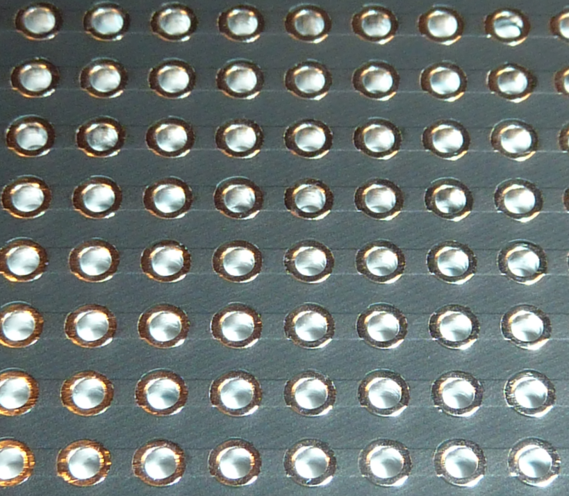
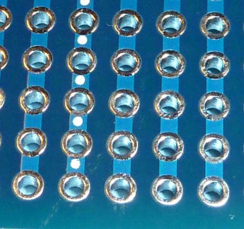
Crack open the KiCad layout tool. Modify a Pin Header footprint having 2.54mm pad spacing and make it long enough to just fit in 10cm - that works out to 38 pads. Then, replicate on a 2.54mm grid to fill 10cm. e.g replicate 38 times to fit inside a 10cm square board. On one side, connect all the pads across horizontal rows with 0.8mm tracks (the purple in the image below). Add the edge cuts, top and bottom solder mask.
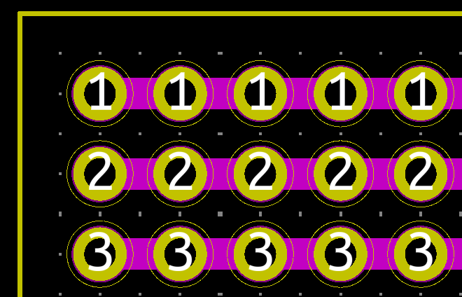
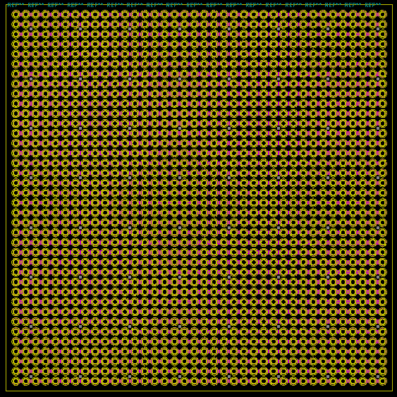
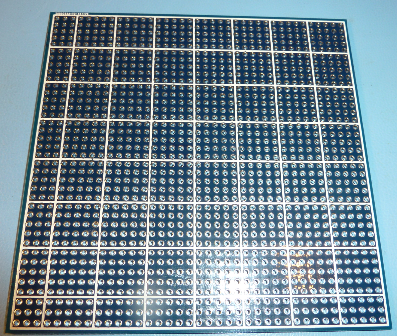
Et voila, 10cm x 10cm stripboard. You'll end up with a really boring layout that looks like this.
Generate the Gerber files and upload to the board shop. Gerber files here. Fill out the manufacturing parameters. Of course, the most important parameter is PCB color. I chose Matt Black thinking it would look cool. (more on this later... not a good choice)
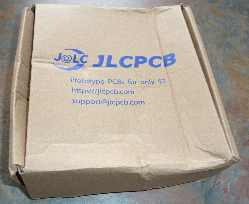
3 weeks later...knock, knock. "sign here sir"... and then, the unboxing !
A little beaten up by Canada Post
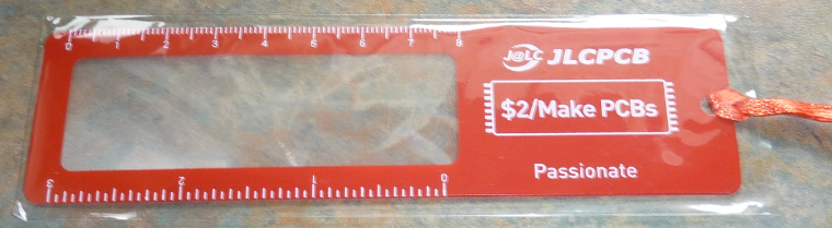
And a bonus magnifier too !
I'm not a PCB expert, but the quality seems decent. Holes are drilled mostly on-center. Plating looks good. Solder mask is where it should be. Only thing... it's really hard to pick out the connection tracks. You need a magnifying glass to find them. Matte Black: not a great choice - it hides the tracks. So much for being cool. Next revision: Either change to a color (green?) or add screening to show where the tracks reside, or both. Adafruit Perma-Proto nails it. I'll learn from them for next time.
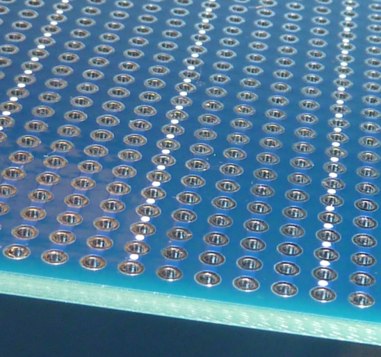
If you look closely you can pick out the connection tracks
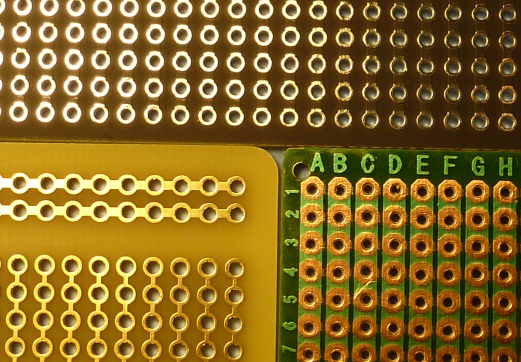
A comparison versus Adafruit Perma-Proto (lower left), Ebay stripboard (lower right)
Got to get the Digikey ruler in a photo ...
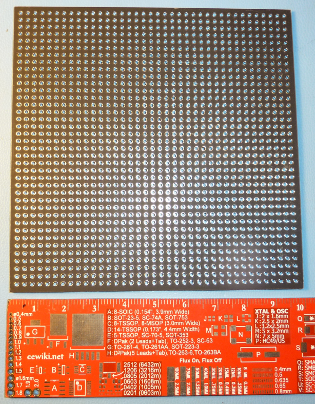
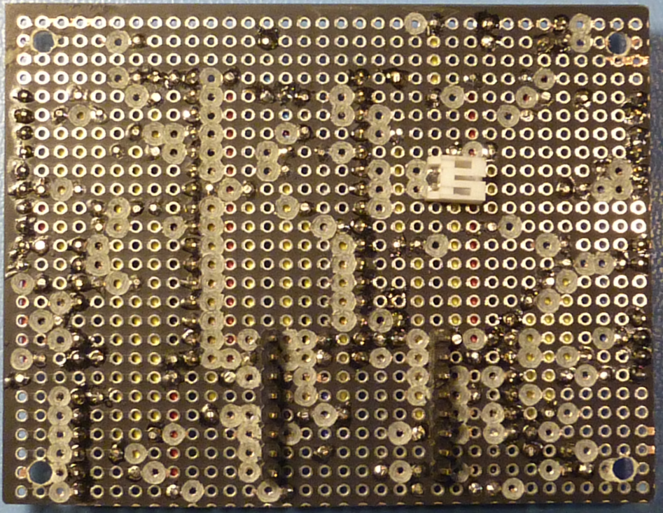
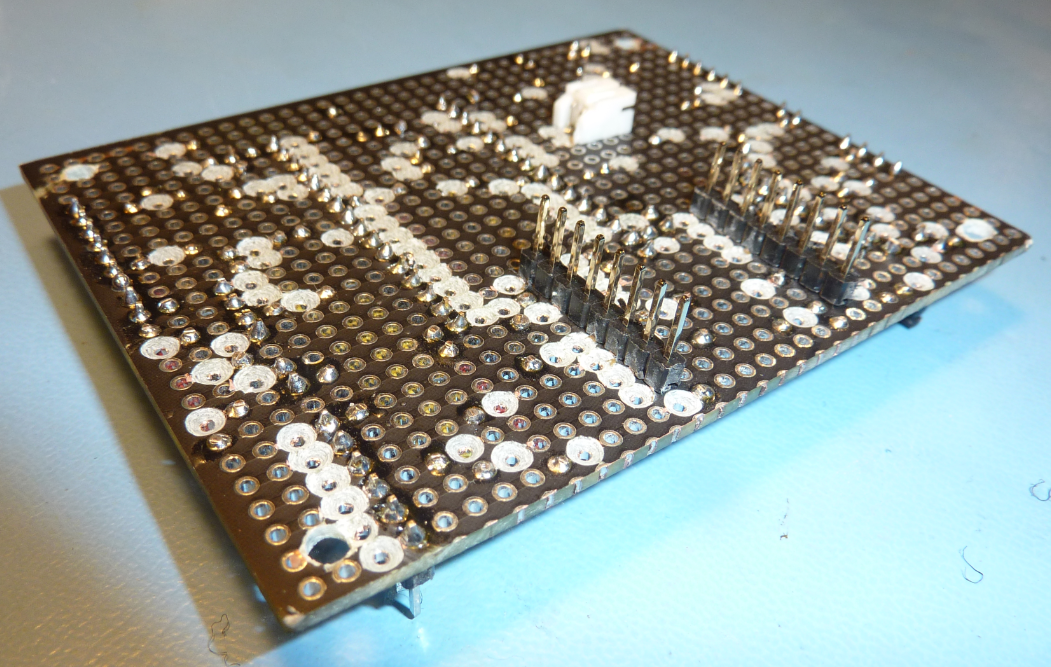
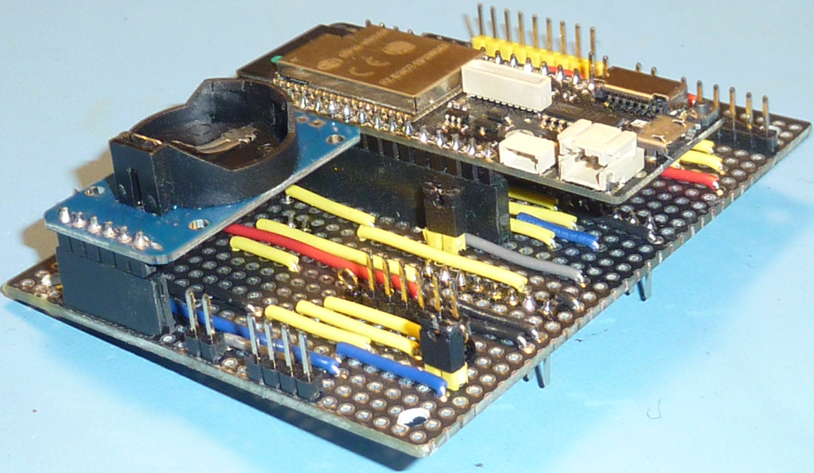
Stripboard layout for a project
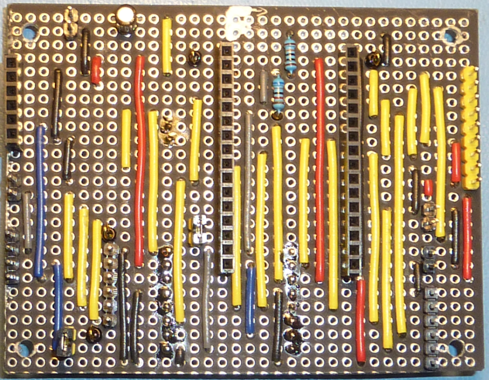
A sensor board for my Street Sense project got the nod for the trial test of this stripboard experiment.
The The Lost Art Of Strip Board Prototyping is a great resource on how to approach this style of prototyping.
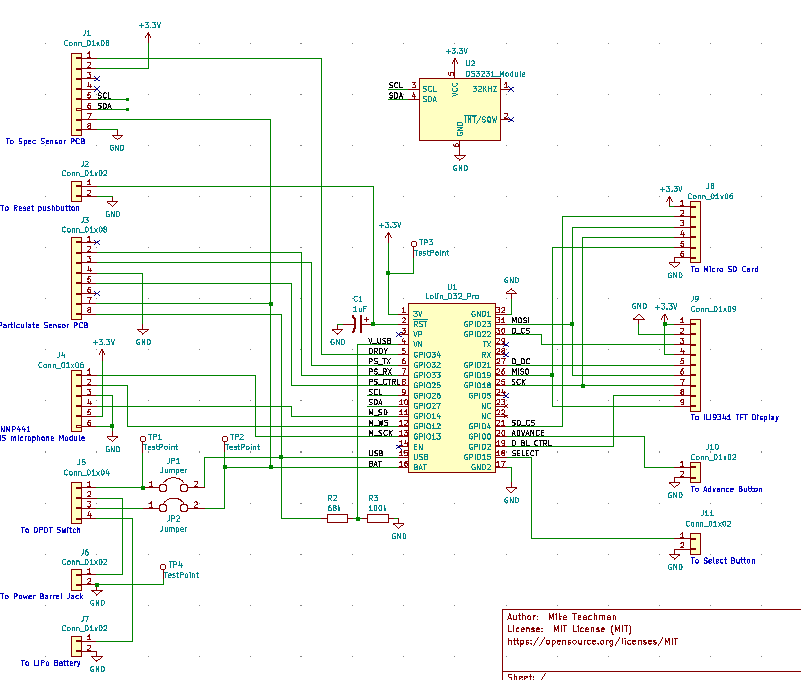
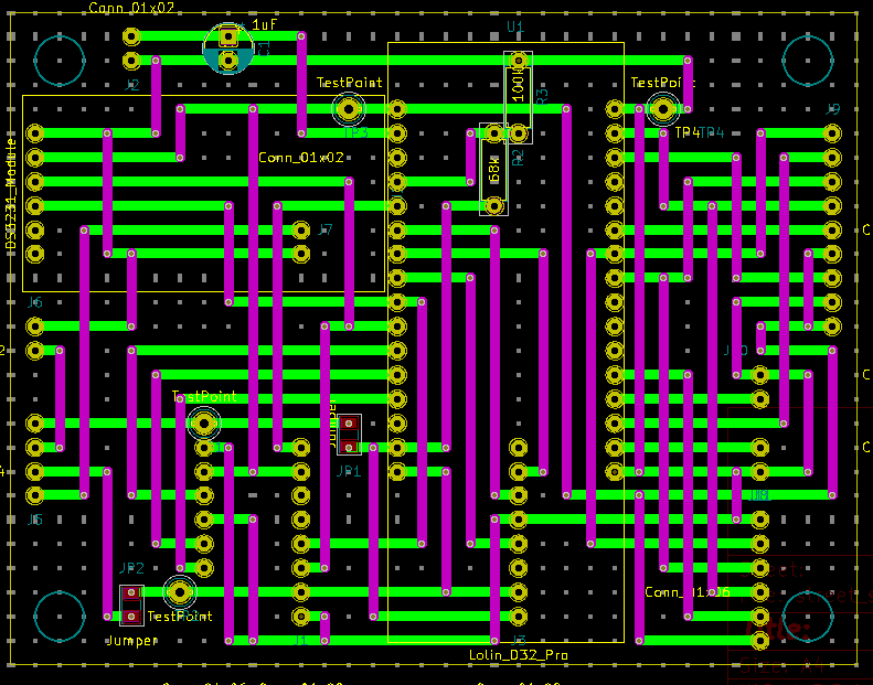
First, the schematic in KiCad. Nothing really interesting here except that it helps to be thinking ahead, knowing that you are locked into a simplistic layout routing - either horizontal (with the built-in stripboard tracks) or vertical with connection wires. It helps to identify your nets by names like "SCL", "SDA", etc. This makes it easier to do the upcoming board layout.
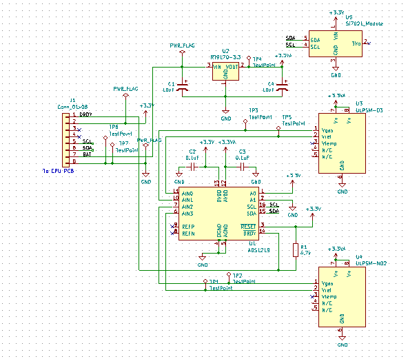
What becomes interesting is how KiCad can be used as an aid for stripboard layouts. Time to hit on the Googles and see what has already been done. I dug up these two excellent references:
Designing professional looking stripboards using Kicad
Design a veroboard/stripboard layout from an Eagle schematic
I followed the instructions in these references to layout the stripboard design. I had to design a couple of footprints as well, for the modules such as the Adafruit Si7021 temperature/humidity...
Read more »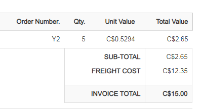


 PCB designer
 Michael Delaney
 Ian Dunn
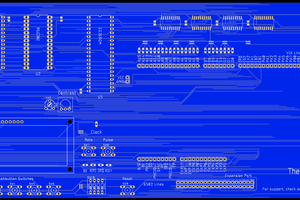
 Josh Kittle
Nice idea. But why do you drill out the holes? I just cut the traces between the holes with one of those snap-off blade utility knifes. Two cuts about 0.3 mm apart allows you to remove enough copper to make sure there is no connection left.