-
Conclusion
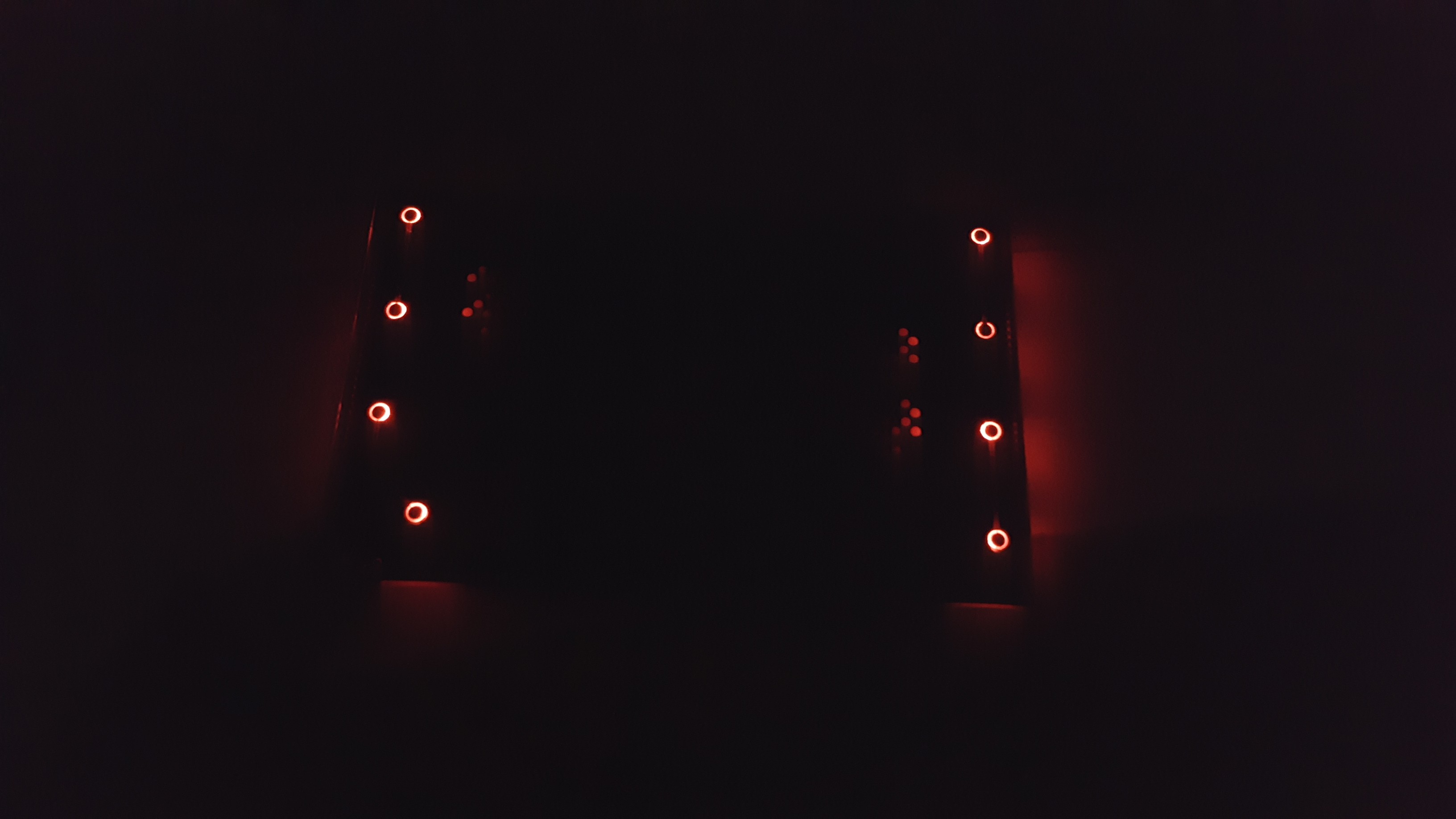
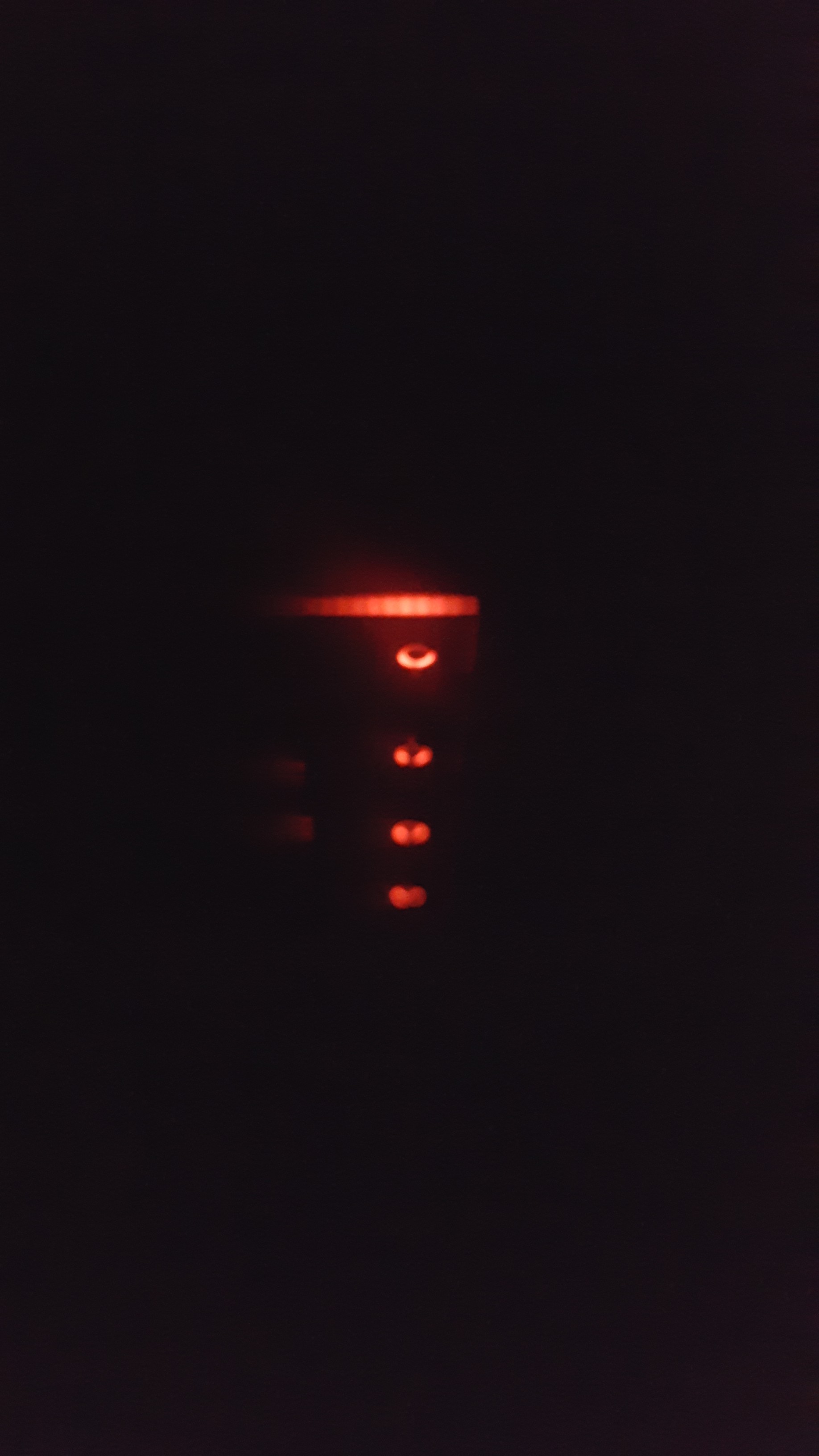
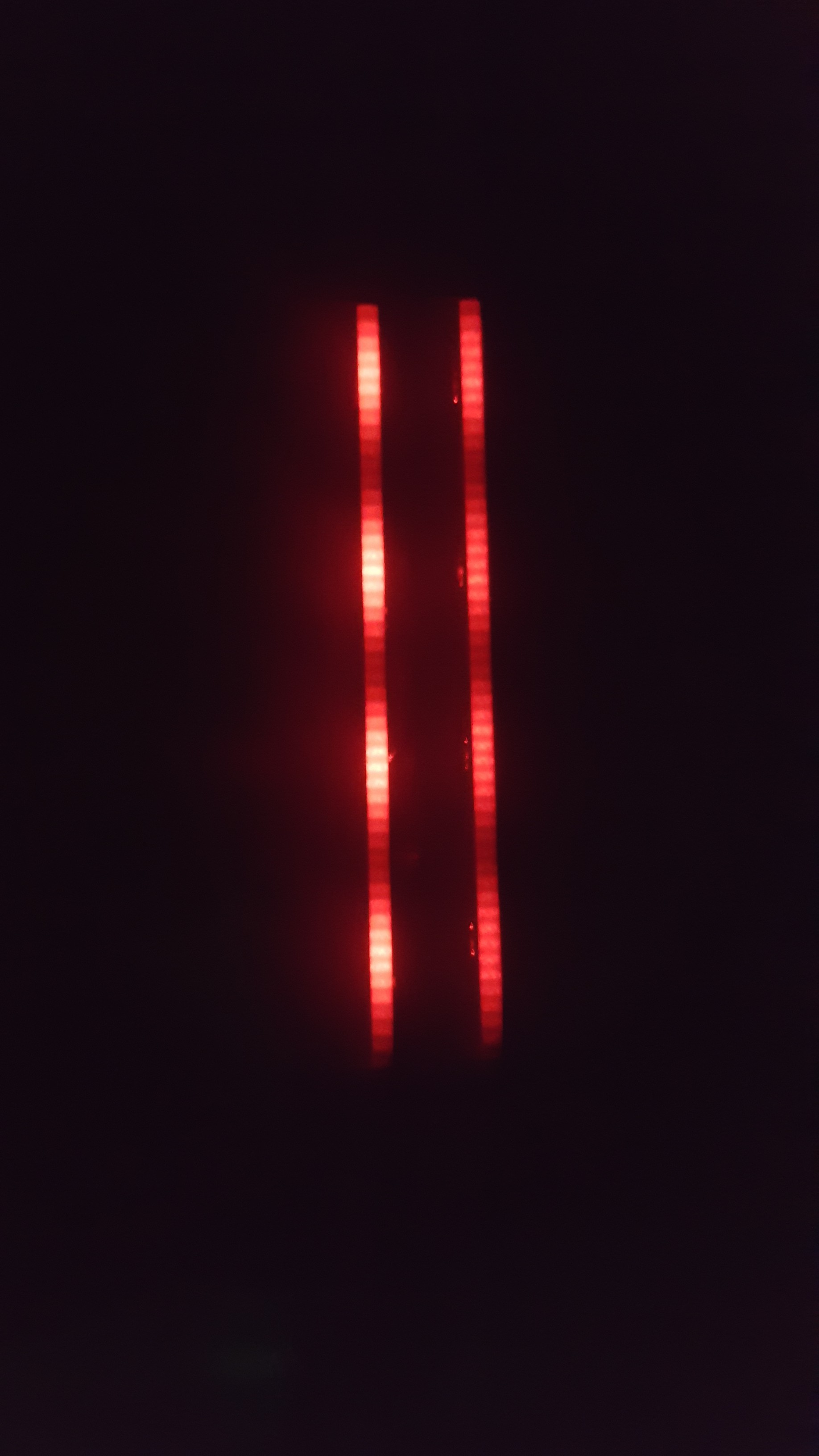
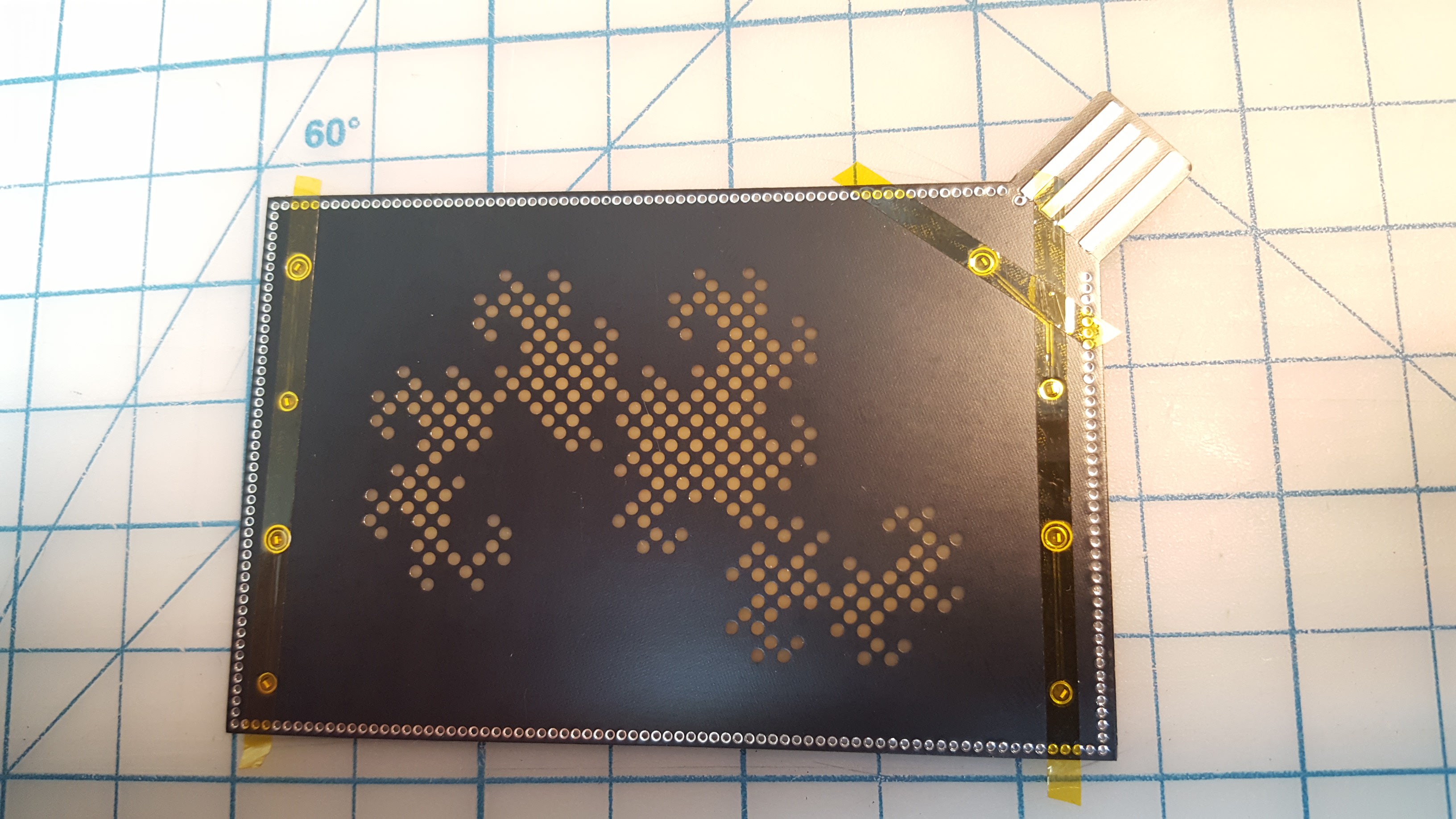
08/13/2019 at 05:44 • 1 commentThis rev of the board did not perform as expected. Although the via wall appeared to successfully redirect the majority of the light into the FR-4, illumination only occurred within 15mm of the LEDs.
![]()
![]()
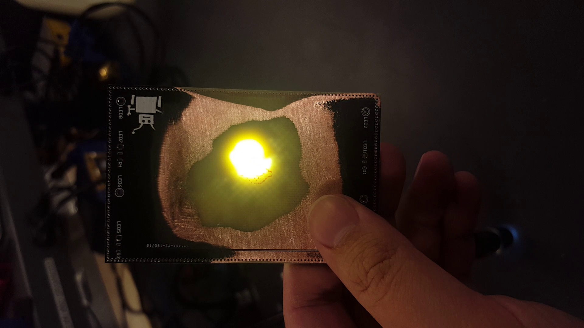
Edge view As a test I pressed a powerful external light to the front surface of the board but was unable to see any light emerging through the empty NPTHs. I also removed a portion of the bottom copper pour using sandpaper to observe the translucency (mp4).
![]()
In another test I installed the LEDs facing outwards to judge how effective the via fence was.
![]()
Left, LEDs facing ourward. Right, LEDs facing inward. FR-4 apparently absorbs a lot more light that I thought. It doesn't seem like all that much when an LED only has to go through 1.6mm of it but in my tests 15mm was the limit of transmission with the aid of the copper pours. I estimate each LED was putting out a third of a lumen, so the entire board had about 2.6.
Fiberglass is an anisotropic material but I'm not sure how its optical properties change with orientation to the weave. Would light travel any better front-to-back through a PCB 10x as thick? It seems like the glass fiber would absorb less light than the epoxy since glass is kinda known for its transparency but there's a lot more scattering surfaces parallel to the fibers so light transmission might be worse in this orientation. Transmissive properties may differ with wavelength as well.
In a future rev I would like to try cramming an unreasonable amount of LEDs into the board but I think this method of illumination is a dead end. The ultimate limit is the thermal dissipation possible with 0603 LEDs that are buried inside FR-4. Larger (and brighter) packages will not fit within the 1.6mm PCB.
The oreo construction method might prove useful for other projects and should be explored further.
-
Assembly
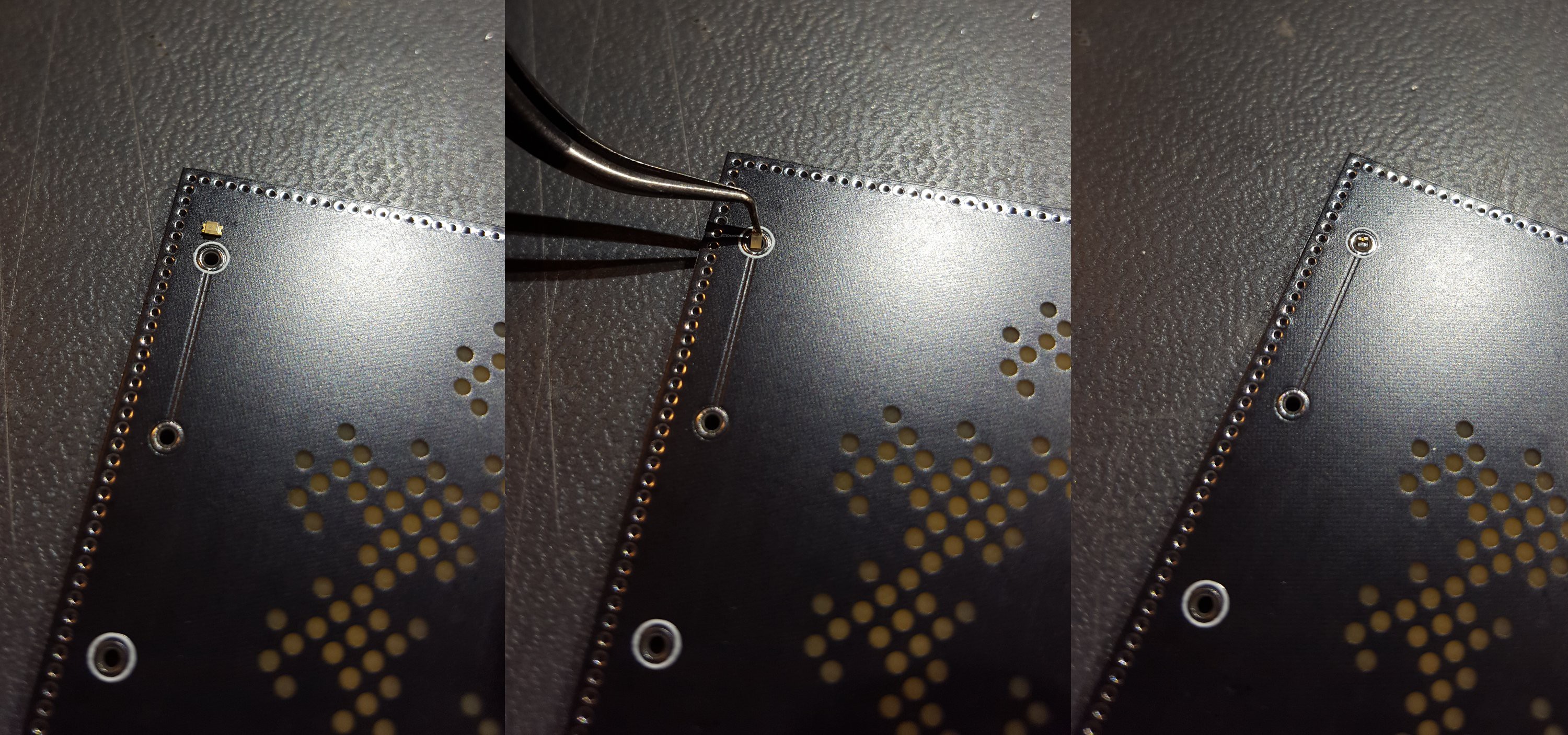
08/13/2019 at 05:27 • 0 commentsAssembly of the board was straightforward. LEDs fit easily into their holes as long as they were aligned normal to the surface. Friction was sufficient to hold them in place before soldering, even if the board was lifted.
Care had to be taken while soldering to ensure the solder successfully made contact with the component leads and did not simply dome over it. Diagnosis can be performed with a multimeter in diode mode. Connection to ground pours was difficult despite thermals but it worked well once the copper heated a bit. I cannot recommend using additional flux for these components as the off-gassing causes the cavity to pressurize while the final solder cap is cooling and it will pop like a bubble.
![]()
Installation of the oreo LEDs. This was a test fit, the final position had the LED rotated a little to point more directly toward the center of the board. ![]()
This tape turned out to be unnecessary, the LEDs are held in just fine by friction. -
Fabrication
08/13/2019 at 05:05 • 1 commentI went with JLCPCB to fabricate these boards and was very happy with the quality. I emailed them beforehand to ask about how they wanted me to notate NPTHs that went through copper pours (usually this signals a PTH). In the end I added a build note to my documentation gerber which called out the drill diagram and I exported two different excellon files, one for NPTH and another for PTH. I also noted this as a comment on the online order form.
They also honored my request to place order number codes on the back side of the board to keep the front pretty. Due to process limitations they weren't able to drill directly through the copper like I wanted but they added a very small pullback to the annular and drilled through the exposed FR-4 which didn't present any problem for assembly. In the future it would probably be easier to modify my library component to present this part as a standard NPTH surrounded (but not touched by) a ring of exposed copper to preclude the need for all these notes.
 Jeremy Ruhland