Ted Yapo
-
Looking at Stuff
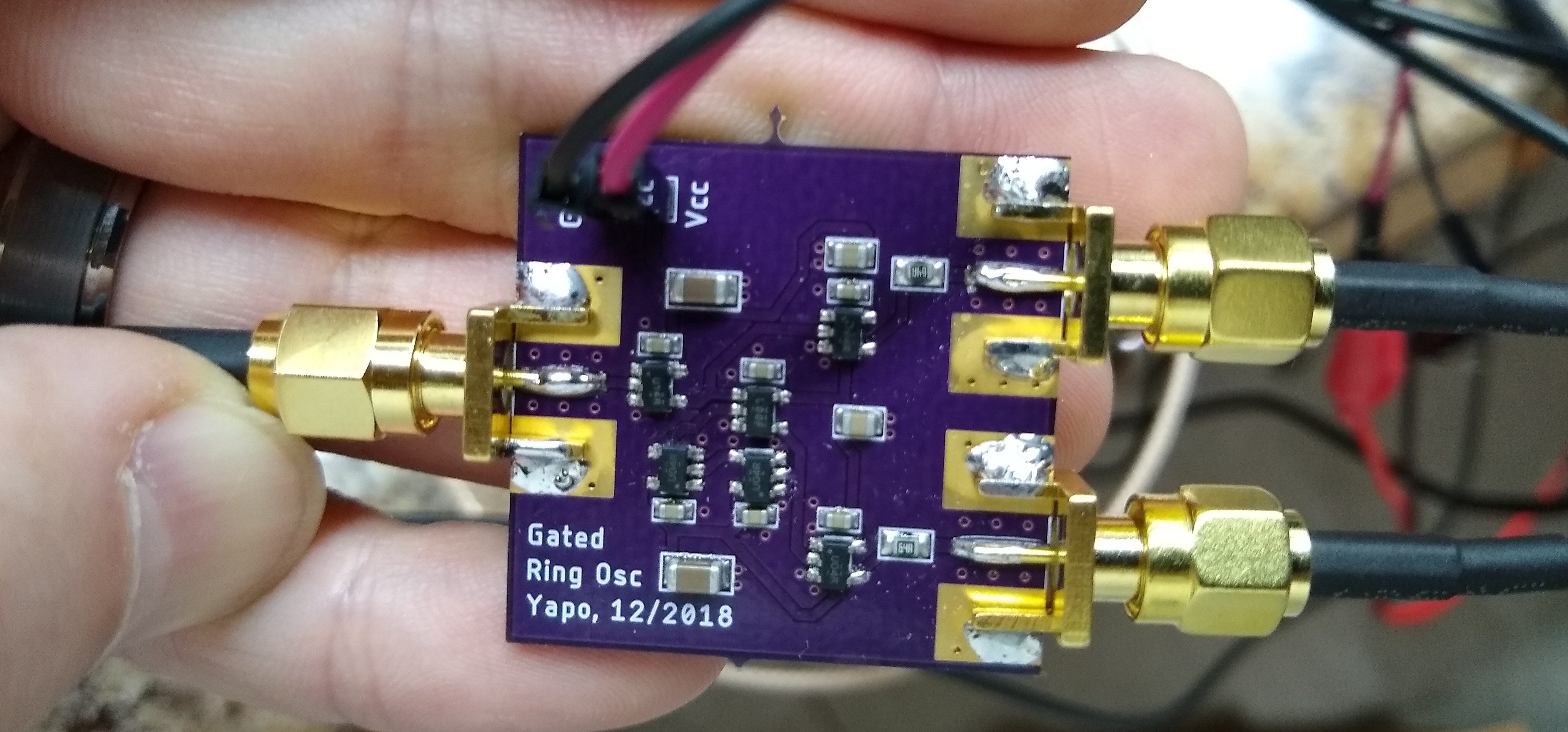
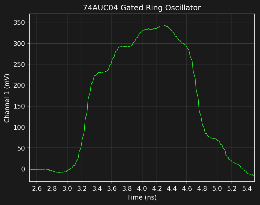
08/25/2019 at 21:01 • 0 commentsAn oscilloscope is for looking at waveforms, so I started digging around for some stuff to look at. I found the 74AUC gated ring oscillator I had discussed on another project, and fired it up. 74AUC logic outputs have interesting steps in their transitions because of their unique 3-stage output driver structure optimized for 50-65 Ohm transmission lines.
![]()
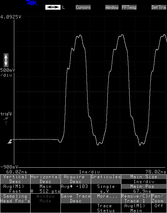
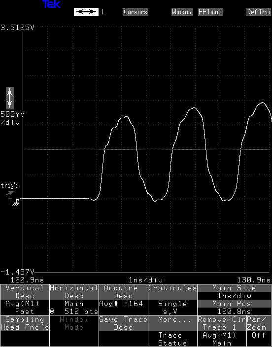
This oscillator, made with very-fast 74AUCxx gates, starts up quickly after the gate input transitions, and oscillates at around 360 MHz. Here is what the output looks like, just after startup, on the 20 GHz Tektronix scope and my prototype sampler of around 6.4 GHz:
![]()
![]()
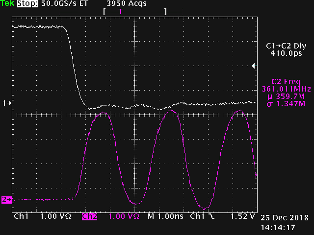
![]() You can see the three-stepped outputs on both scopes, although there is more detail in the left image from the Tek scope, but that's a 20 GHz instrument, so it's not really a fair comparison. Note that on a 1 GHz scope (image at end of log), you can't make out the steps at all.
You can see the three-stepped outputs on both scopes, although there is more detail in the left image from the Tek scope, but that's a 20 GHz instrument, so it's not really a fair comparison. Note that on a 1 GHz scope (image at end of log), you can't make out the steps at all.To get a more apples-to-apples comparison, I ran the Tek signal through a TL-11 delay line. This beast made to accompany the 11801 scope is a 47 ns analog delay line with a 70 ps rise time, which equates to a 5 GHz bandwidth. It's essentially a long, precision coax-cable-in-a-box. This should simulate what the signal would look like on a 5 GHz scope, or so I thought. Here's what you get:
![]()
![]()
![]()
I can't explain the slow rising envelope at all. Ideally I would run the signal through the delay line for both scopes for the comparison, but I can't do that at the moment - the 47 ns delay messes up timing. But, in any case, some of the fine details are lost with this "5 GHz" simulated Tek scope, so it indicates that some of those details probably are above the 6.4 GHz 3dB cutoff of the prototype.
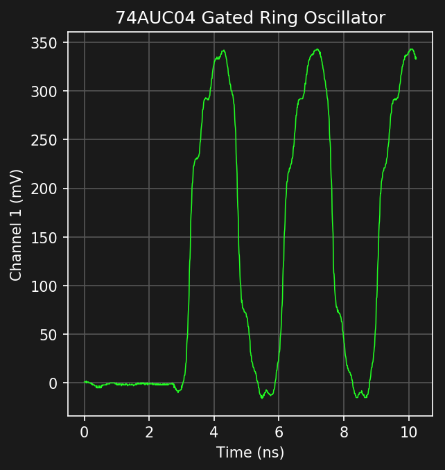
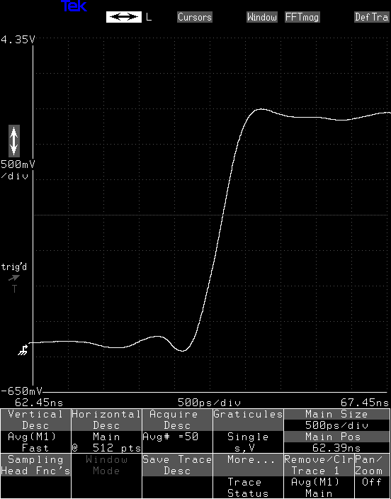
For reference, here's the waveform as I captured it on a slow 1 GHz oscilloscope back in December. With a 1 GHz scope, the finer details of the transitions are blurred, and you can't see evidence of the 3-stage output drivers at all.![]()
Lol - check the date. That's what I was doing on Christmas day at two in the afternoon!
EDIT 20190827
Here's the details of the 3-stage output driver in a 74AUCxx gate from TI's appnote, and a zoomed-in look at the stepped output waveform it produces. The steps are about 200 ps long.
![]()
![]()
At least, I think that's what you're seeing here. I need to put one of these gates on a PCB that just produces a step so I can see what happens later in the transition. Supposedly, the three stages switch over longer periods. Boards have been ordered.
UPDATE 20190828
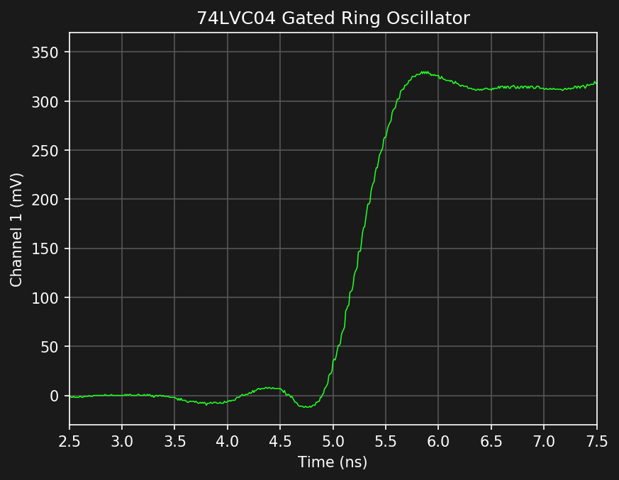
I found another copy of the ring oscillator PCB and populated it with 74LVC parts. These are slower than the 74AUC, but have a traditional 2-transistor CMOS output structure. The transitions don't show the step artifacts, which points to them really being caused by the 3-stage outputs of the 74AUC gates rather than a reflection phenomenon on the PCB. Here are the Tektronix vs my sampler images:
![]()
![]()
![]()
There is less noise in the Tek trace, but it also has been averaged 50 times. I could probably do better than I currently am.
But, I'm still not entirely convinced that I'm seeing artifacts from the 3-stage output drivers in the 74AUC parts. When the new boards come back, I should get a more definitive answer.
-
More Accurate Bandwidth: 6.7 GHz
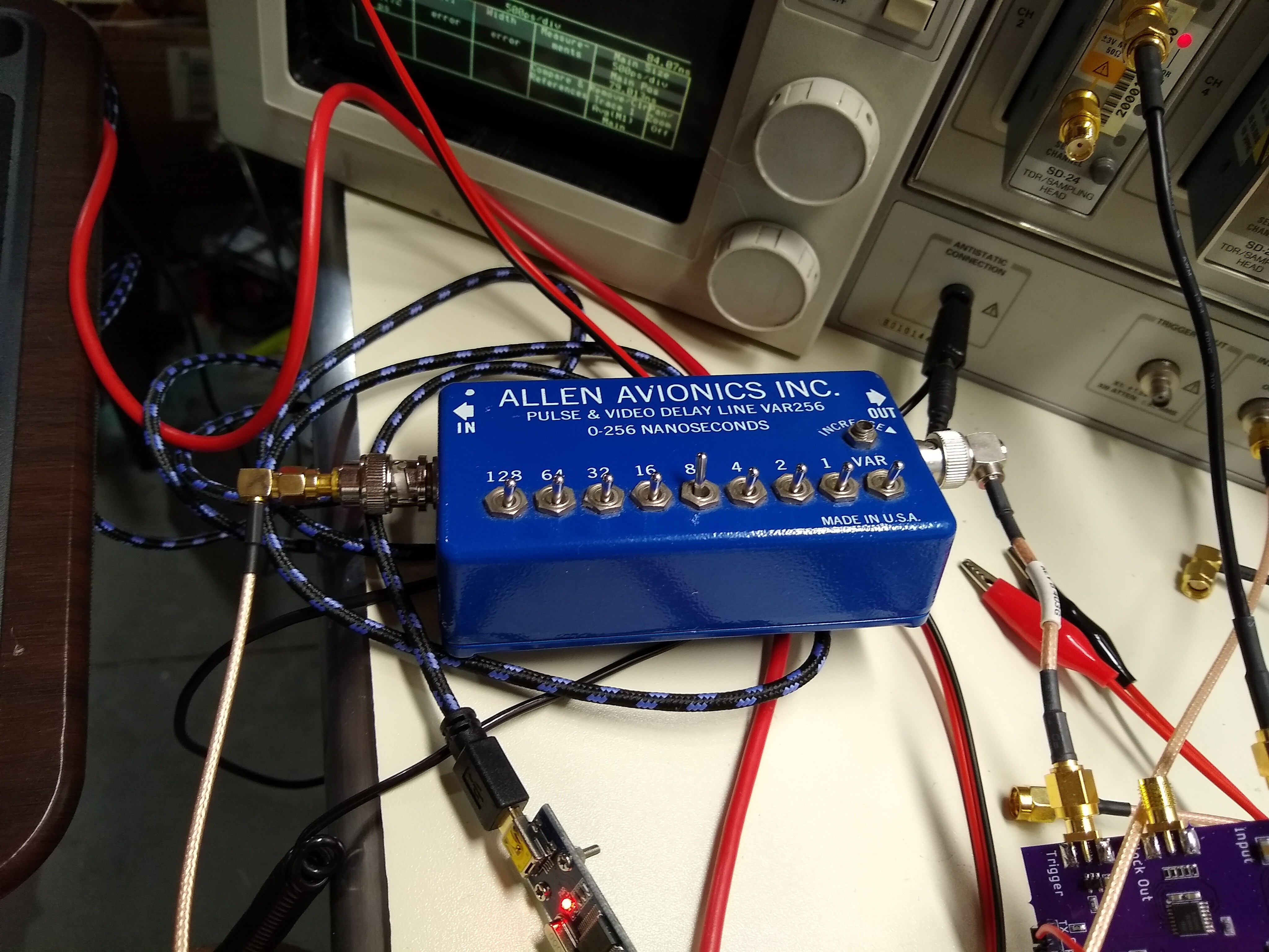
08/23/2019 at 16:21 • 0 commentsIt took a little doing, but I was able to measure the bandwidth of the prototype sampler using the TDR step generator built in to the Tektronix SD-24 head. I had to drag out an old Allen Avionics switchable delay line to get the triggering right.
![]()
This was also the first test of external triggering for the sampler. It worked :-)
The delay line has a very low bandwidth, and even though it's only delaying the trigger pulses here, it can cause problems by slowing the trigger edge resulting in timing jitter. I haven't determined how much of an effect this actually has on the measurement yet, but it can only result in an artificially low bandwidth estimate, so it's OK for now. I really should just cut a piece of low-loss coax to the right length (which appears to be 8 ns) and use that as a delay. Maybe later.
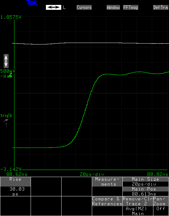
The Tek scope measures the rise time of the TDR pulse as 30 ps:
![]()
This is at the end of a short section of RG-174 cable, which is lousy for this kind of work, but is flexible enough to connect between two inputs on the same SD-24 head. The rise time of the step measured internally to the head is 24 ps.
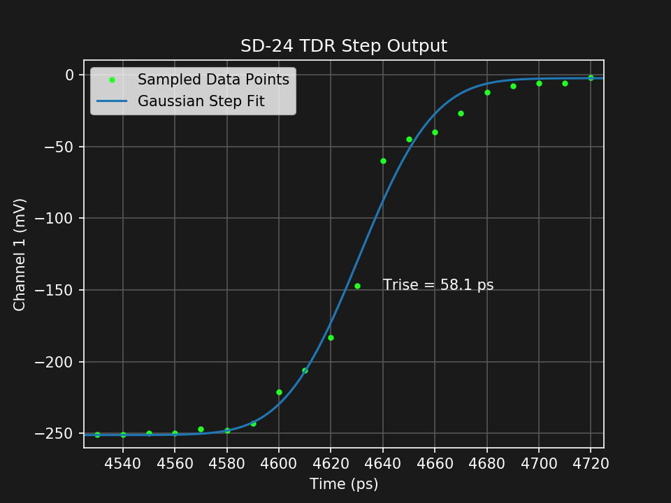
Using the same trick as before, namely, fitting a Gaussian step function to the prototype sampler response, I come up with a measurement of 58.1 ps.
![]()
Again, using the same logic as before, and correcting for the step response of the SD-24 head, the actual step is probably close to sqrt(30^2 - 17^2) = 25 ps.
Using this to estimate the response of the prototype, we get Trise = sqrt(58.1^2 - 25^2) = 52.4 ps.
A scope with a Gaussian response and a rise time of 52.4 ps has a bandwidth of 6.7 GHz.
What did I estimate the first time? (checks notes) oh, yeah, 6.4 GHz. Pretty close.
I'm calling it 6 for now.
I might be able to get some better measurements by averaging more in the sampling process. It might be worth some experiments, but without an accurately calibrated timebase, it probably wouldn't mean all that much.
-
What's the F̶r̶e̶q̶u̶e̶n̶c̶y̶ Bandwidth, Kenneth?
08/23/2019 at 15:47 • 0 commentsIn the initial testing, I tried several approaches to estimating the bandwidth of the first sampler.
ADCMP606 Step
The ADCMP606 step generator was the first experiment over on #The Rise and Fall of Pulses , and in some ways the most successful. It just uses an ADCMP606 CML-output comparator to generate a moderately fast rise-time step, typically 160 ps according to the datasheet.
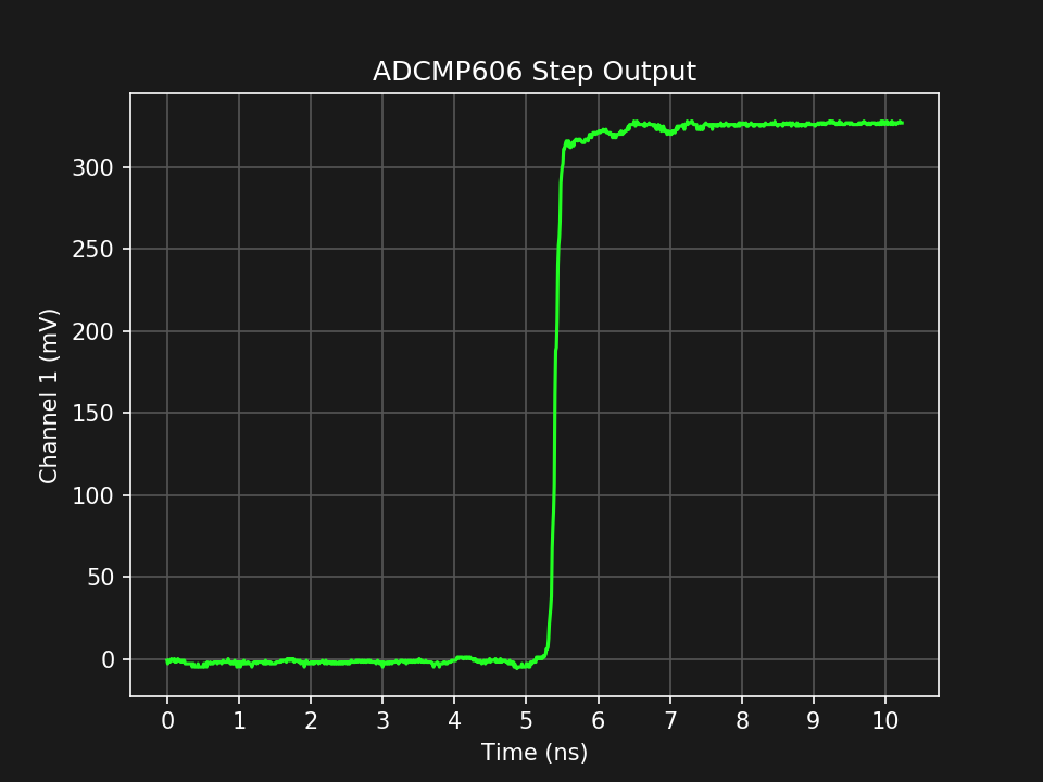
Here's the output measured with the sampler:
![]()
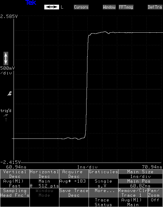
and with the Tek 11801B/SD-24:
![]()
The traces look similar, but again they were triggered slightly differently, which could cause some discrepancies. The differences right after the edge are most likely caused by some reflections from the sampler itself. Matching on the front-end needs work.
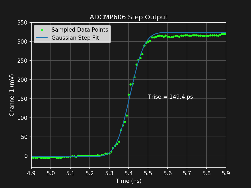
To estimate the sampler bandwidth from this, I fit a Gaussian step to the data points, and calculated the rise time of the fit function:
![]()
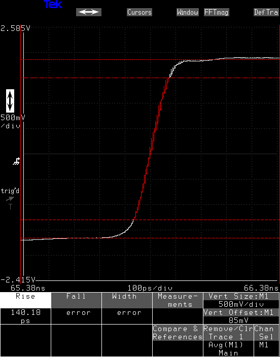
The Tek scope measures the same 10%-90% rise time at 140 ps.
![]()
The SD-24 head has a maximum rise time of 17 ps, so the step from the ADCMP606 is probably closer to sqrt(140^2 - 17^2) = 139 ps. From this, we can estimate the rise time of the prototype sampler = sqrt(149.4^2 - 139^2) = 55 ps.
A 55 ps rise time for a scope with a Gaussian response implies a bandwidth of 0.35/55e-12 = 6.4 GHz.
-
First Measurements
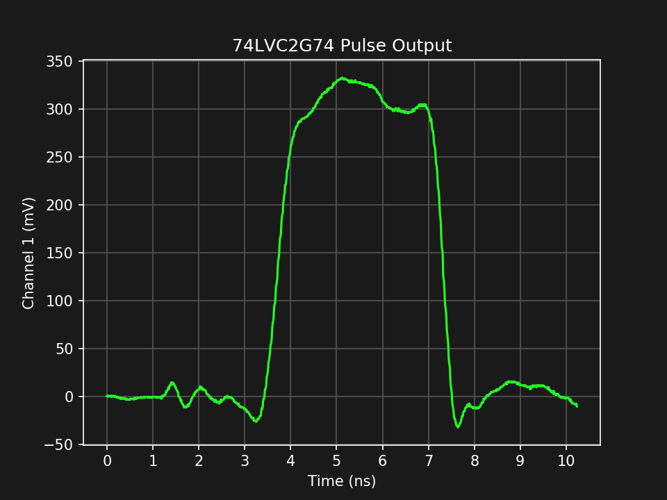
08/23/2019 at 14:31 • 0 commentsI have been told that at a certain oscilloscope manufacturer the first measurement with a new scope design is sometimes called "green on screen," like "first light" for telescopes and "first ping" for routers. This is the first waveform captured with the first prototype sampler:
![]()
It's the output from a pulse generator made with a 74LVC2G74 flip-flop with the data line tied high and Q-bar output tied to the Reset-bar input. I'm using a pulse generator like this (but with faster 7 4AUC logic) in another sampler design. Don't use this in your logic circuits, people, it's just for analogy-stuff :-)
![]()
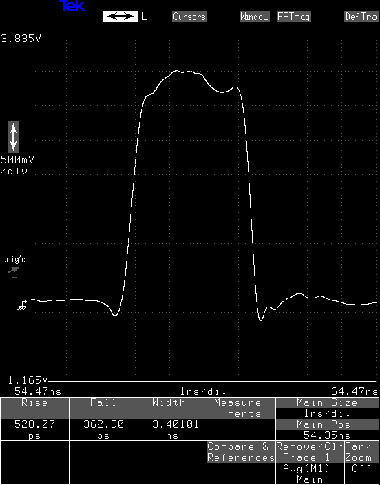
For reference, here's the output of the same circuit captured with a Tektronix 11801B scope and 20 GHZ SD-24 head:
![]()
There is an extra wiggle on the left baseline of the trace from my sampler. The test setup to capture these two traces was not identical, and I suspect there may be a ground-bounce issue causing the difference. It needs some further investigation.
Overall, however, the result doesn't look too bad for a first test. The waveforms are pretty close otherwise, and the result would certainly be usable in some cases. I know there are some reflections happening in the front end which are sure to corrupt the waveform somewhat, and these may be responsible for some of the small differences here, but I think the result shows promise.
-
Overview and First Prototype
08/23/2019 at 13:23 • 2 commentsThe scope works using a comparator to sample the input waveform. This is an old idea, which seems to date back to S. P. McCabe III's Masters Thesis in 1975, "A sampling voltage tracker for analyzing high speed waveforms." I haven't read it yet, but next time I'm in Los Angeles, maybe I'll swing by UCLA and have a look.
This approach was finely honed by a team at NIST, who wanted to use such a sampler for high-resolution measurements of RF waveforms, initially to replace thermal sensors in true-RMS-reading RF voltmeters. Since the NIST work is US-Govt. funded, the papers they published are not protected by copyright. Here's a good introduction, highlighting some of their latter work on the idea.
The basic idea is to capture a single comparison result at each trigger. So, at the first trigger, you ask if the waveform at the trigger time is above or below a specific voltage. By trying a number of voltages, and recording the greater/less-than answers from the comparator, you can eventually deduce the voltage at that time. If you've ever explored successive-approximation analog-to-digital converters, you'll recognize a similar process. Unfortunately, the binary search used in most SAR ADCs is sensitive to noise, and is not always suitable for a sampling oscilloscope. There are a number of alternative approaches, and a small body of literature on research in this area. The simplest (and perhaps slowest) method is just to try all possible voltages. It's dumb, but it works, and is resilient in the presence of noise.
Schematic
I'm just going to link the PDF schematic here. The ADCMP582 comparator is the front-end. An MCP1501 2.048 V reference, MCP4921 12-bit DAC, and ADA4000 op-amp form the reference voltage generator that the input sample is compared to. The reference voltage has a range of -2 to +3 V, covering the entire input range of the comparator. In future versions, this may be reduced to +/- 2V. This DAC uses SPI and is relatively slow. I'm currently evaluating faster, parallel DACs.
I swapped op-amps at the last minute in the design, and accidentally connected the inputs backwards (doh!), so these are incorrect in the schematic and board layout, and the board requires a little rework to swap these pins before it will work correctly.
An SY89296U programmable delay line handles timing of the samples. This allows 1024 different sample points, spaced nominally 10 ps apart, for an equivalent time sample rate of 100 GSa/s. On the first sampler prototype, this timebase is uncalibrated. I have a prototype timebase calibration board which has proven a way to calibrate the timebase, and it will be intergrated into the next version.
Since the comparator and delay line are ECL parts, there's a little ECL interface logic to connect to the CMOS parts of the design.
The brains of the PCB is a PIC16F15376 8-bit microcontroller. I chose this because of familiarity with the 8-bit PIC world and previous experience with the built-in peripherals. The inclusion of a 32-bit uC here wouldn't accelerate the design much and simply add complexity to this first prototype. The next spin currently has an FPGA to handle anything that should go faster.
Another key component is the Si53360 clock distribution buffer. This CMOS part handles the clock and trigger timing while adding very little jitter (120 fs RMS). The two inputs to the clock fanout part allow the sampler to be triggered from an external source, or to generate its own sampling clock. This functionality directly parallels the Tektronix 11801 sampling oscilloscope. It works pretty well.
Board Layout
Again, a link to a pdf of the layout. This first prototype was put together quickly to get some data before a next spin, so it's a little rough. At these speeds, though, there's no substitute for measurements with the actual device, so it makes sense to build and test early and often. This is just the first prototype which contained enough stuff to make actual measurements.
The board is a 4-layer design fabricated at OSH Park. One of the three PCBs I received seems to have a short between two internal layers, but I haven't fully tracked it down yet, so I'm not pointing any fingers. Besides, to make a good footprint for end-launch SMA connectors, you are forced to violate the design rules, especially about copper pullback at the board edges.
A key piece, and probably one I don't have quite right yet, is keeping the power supplies quiet. I have two separate regulators for the 3.3 V supplies for the ECL and CMOS parts of the design, but this in itself is probably not sufficient. One of the tasks for the next spin is to take a very close look at the power distribution network with an eye to reducing jitter.
8 GHz Sampling Oscilloscope
8 GHz BW, up to 1 TS/s ET Sampling I have ceased active development on this project. Please don't ask.