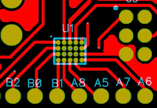
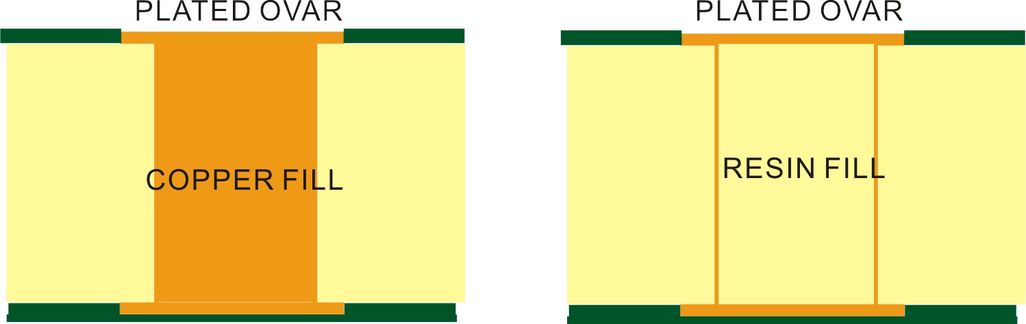
Via in PAD
Connect via in solder pads is a big trouble in pcb assembly process.
Especially,when the via in BGA pads,
But the designer often based on its design can not achieved.
In face,the electronic products is getting smaller,
printed circuit board going to smaller, high density and more layers,so,many CAD Engineers( PCB Layout engineers) design the via in pads.In particular,small BGA ball space of BGA Pads,there is no enough place
Could place the via holes.It is disaster for SMT engineers.With the improvemet of via in pad technology,The solder problem can be solved.
Capabilities
Capabilities
Smallest Hole:4Mil(Laser) 6Mil(Machine)
Smallest BGA: Holes+6Mil
Aspect Ratio:1:1(4Mil) 12:1(other)
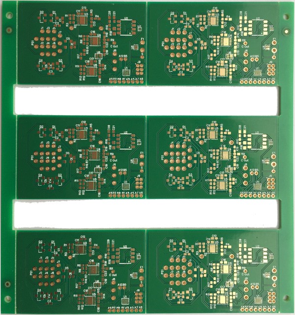
Product
SPECIFICATION:
Material:FR4
Thickness:1.6mm Copper:1OZ
Surface Finished:ENIG
Layer Count:2Layer
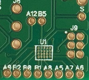
DIFFICULTY:
Via in BGA
Holes:4Mil BGA:10Mil
Finished Board Thickness:62Mil
Aspect Ratio:16:1

 MagicWolfi
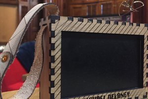
 Michael Delaney
 gokux
gokux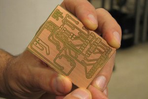
 PCB designer