blinkingthing
-
Assembling and Testing v2.2 PCBs
10/11/2019 at 23:29 • 0 comments![]()
Assembly Plan / Prep
While waiting on the components to arrive from overseas, I made a cheatsheet for assembling my board. I saw someone else do this for use when assembling diy ANDnXOR DC24 Bender badge's and found it to be helpful.
![]()
Received Parts
Most of the components came from LCSC but some that weren't available there came from Digikey. I've had the brass tube in stock for a while but I ordered that through Amazon a few months back when I started experimenting with it.
Actual Assembly
The assembly for these badges was inspired by watching dr_n0pesl3d's twitch streams where they used a hot air rework tool to solder components one at a time. I had never seen this before and didn't recognize it as a possibility. I thought you only re-worked previously soldered components, or used an oven the reflow everything on the board at once. This concept of using the hot-air tool to assemble boards one component at a time wasn't a concept that existed in my head previously. Placing the solder paste with the syringe for each individual component is probably my least favorite part of this process as I'm inaccurate and wasteful.
![]()
Assembled and flashed before bond wire installation Moment of Truth - Plugging in USB.
After I got all the components on the first board I wasn't really sure how to go about testing it before plugging it in and taking it for a spin. I ended up visually inspecting all IC's and the USB connector for any bridges/shorts. After cleaning those up I used the breakout pins and a multimeter to test neighboring pins on the EPS32 to double check for bridges/shorts. Once I was semi-confident that nothing was going to be destroyed when I applied power, I plugged it in.
I could not believe that it didn't go up in a puff of smoke as soon as it was plugged in.
What Works What Doesn't
I had a bit of troubleshooting to do as nothing really happened when I plugged in my board aside from the power indicator LED lighting up (which was still sort of cool cause I've never powered anything through USB before). It turned out both the CP2102 and ESP32 hadn't completely/correctly reflowed. I ended up having to hand solder all 5 of the v2.2 badges I made because I couldn't get them to completely reflow correctly using the hot air tool I have. I assume I'm not heating up both the pixel badge board and the ESP32 WROOM board in close enough synchronicity to correctly reflow it. I've gotten a handle on the CP2102's QFN package now, but it was the most difficult chip I've soldered in my electronics career thus far.
Indescribable Feeling of Uploading something directly through a USB Port
After I got the ESP32 and CP2102 installed correctly, I plugged in the badge via USB and checked out the list of USB devices on my computer. Seeing the a UART chip by Silicon Labs listed in my list of USB devices gave me a rush of excitement that I don't feel often. I know it's probably trivial to most people more heavily involved with the hardware world, but this felt like unlocking a door that l've been stuck behind for a while. It make's me feel like I might be capable of designing and manufacturing actual electronics.
![]()
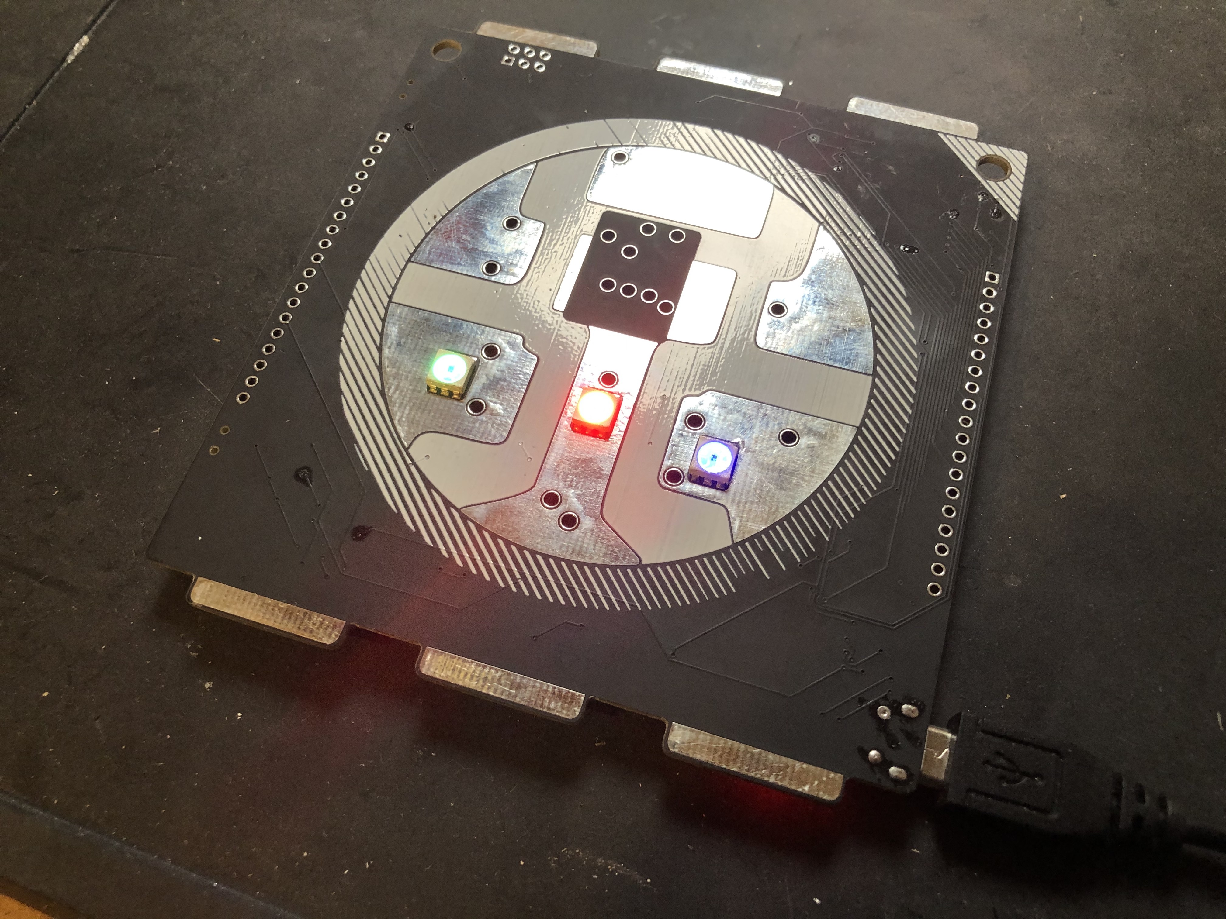
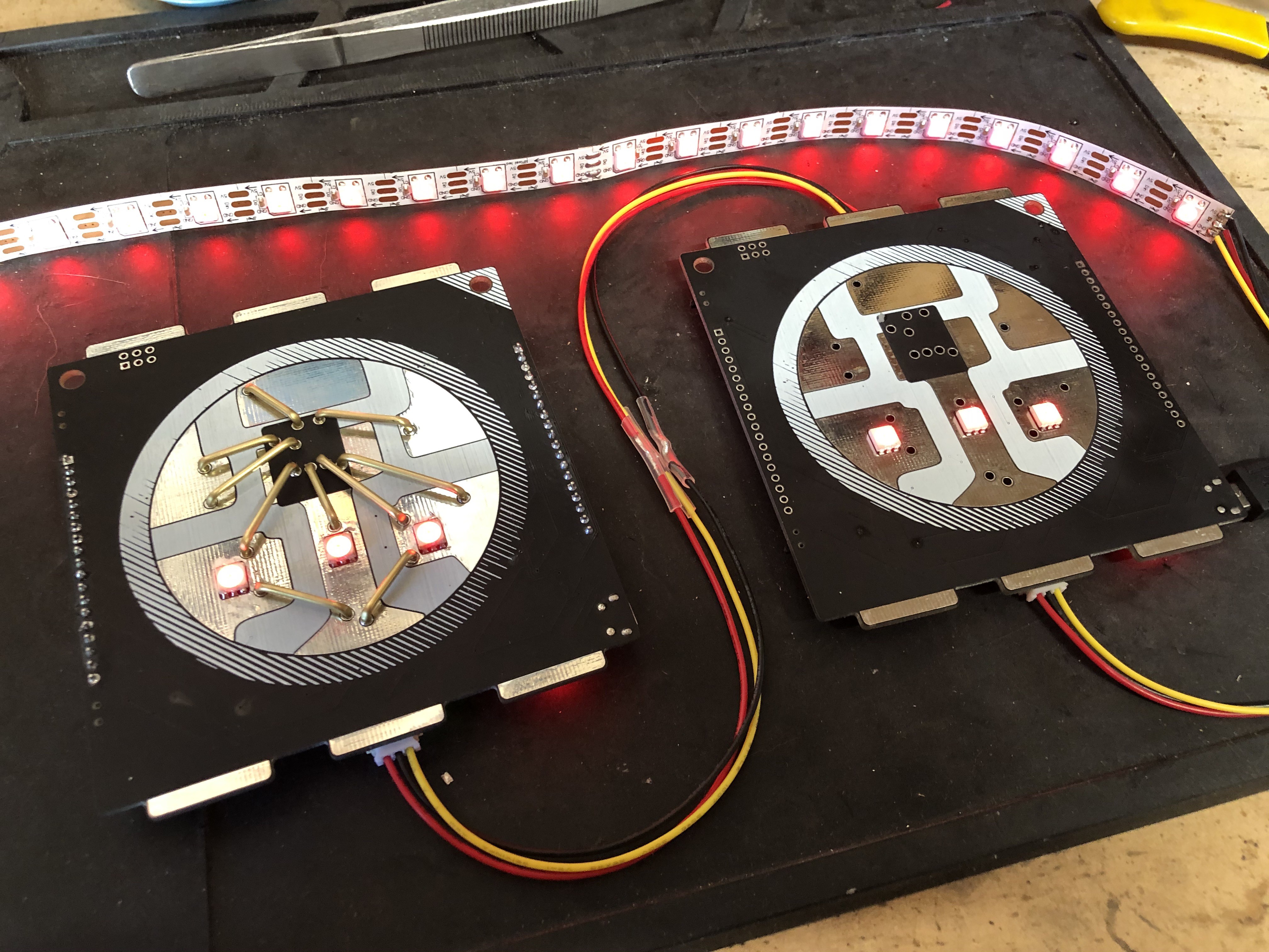
Notice the R G B indicator lights and green bodge wire. Battery Hissing
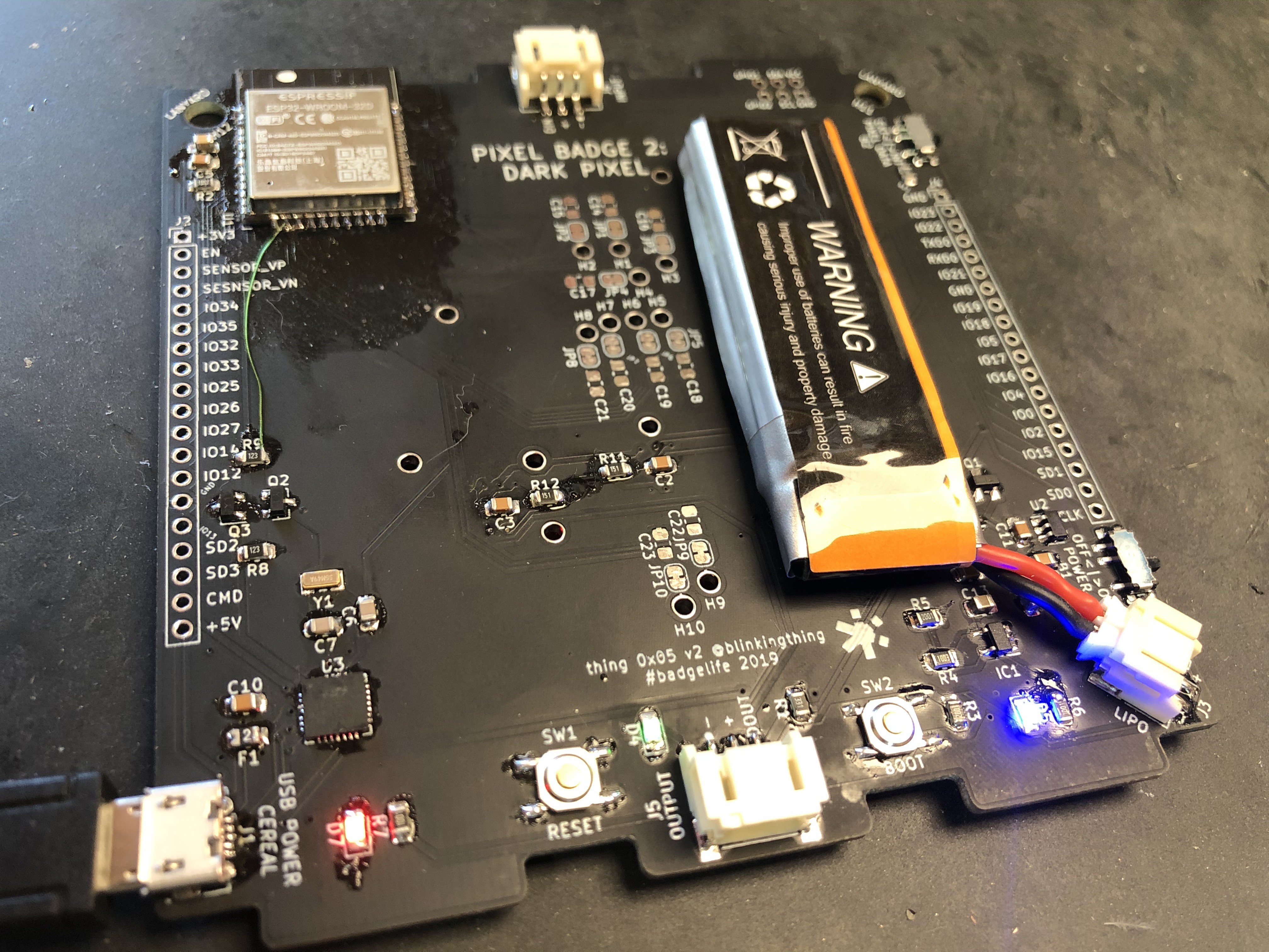
One of the major components to check was the LiPo battery charging circuit. When a LiPo is plugged in and charging, there is an extremely quiet and high pitched whining/screeching/hissing sound that emanates from the board. I can't tell if it's the actual battery or some of the components on the board making the noise. This is the scariest part of the build for me because I copied the schematic, don't understand it electrically, and now have a potential problem to figure out. I double checked the schematic and components and I don't think I did anything wrong. I let the battery charge (outside) for 3/4 hours and it never exploded or caught on fire, nor did the battery start to expand or anything like that. So for now, I think it's safe, but not 100% finished.
Auto-program circuit broken (Good Thing I have Buttons)
Another part of the circuitry that needed troubleshooting was the circuit that is supposed to automatically put the ESP32 into boot loader mode so you can upload code to it without the need to press any buttons or jumper anything. It doesn't work. Luckily, I copied the buttons from the schematic that allow me to get it into boot-loader mode manually. When I double checked my schematic that I copied from the Hornbill dev board, I realized I didn't connect the RTS pin within the auto-programming circuit to IO13 on the ESP32. I tried making this connection with a bodge wire on the board and tested the auto-program circuit again and it seems like it got one step further, but still didn't successfully get into boot-loader mode. I only know that it progressed a little because all the neopixels turn bright white on the breadboard version of this badge when the auto-upload works. When I added the bodge wire, the neopixels turn white when I go to upload, but the connection is never completed. I'll be sure to figure this out before the next version of the board.
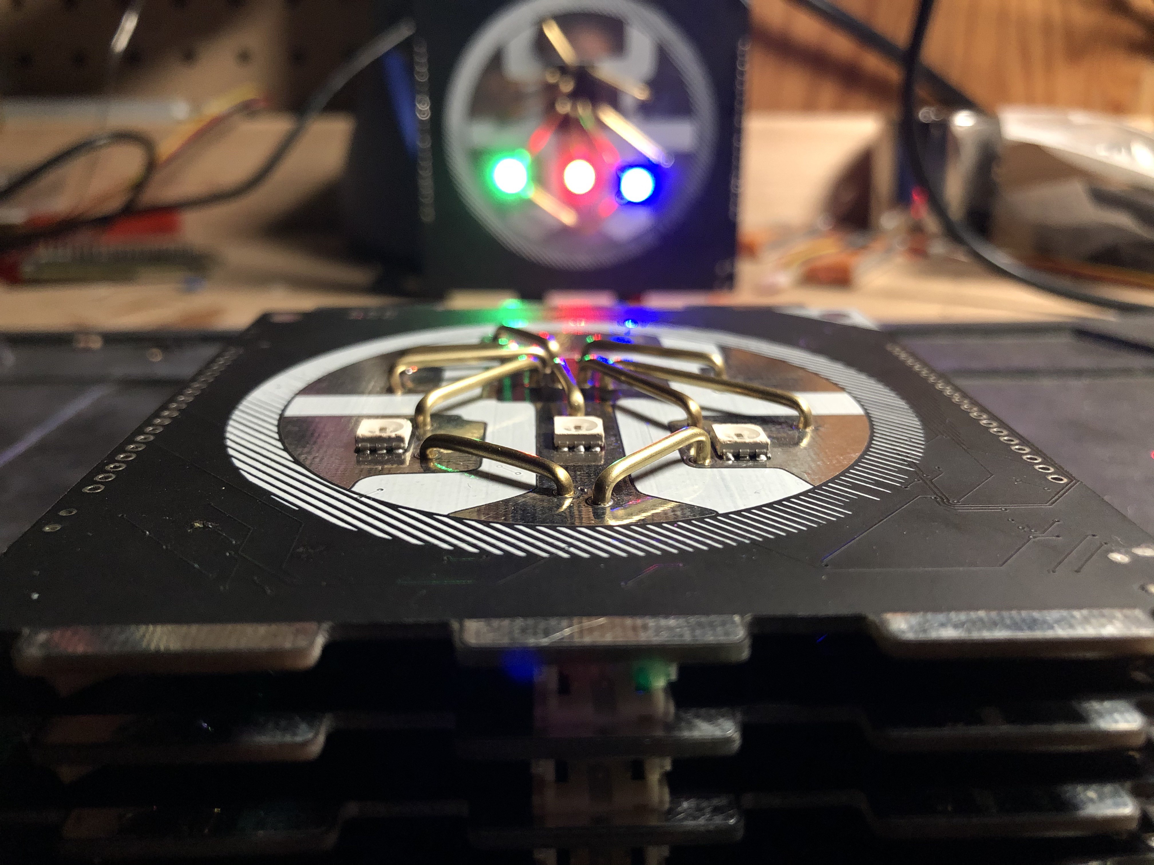
Daisy Chaining Details
Daisy-chainability was one of the main features I wanted to implement and I'm glad to report to that it works! Right now, each badge has an output with 3.3v, GND and DOUT for the Neopixel chain. The inputs however only take in GND and DIN. I was unsure of how to handle taking in power from an external source and it's one of the major items on my to-do list. I also have to think about this badge running at 3.3v and the conflicts that will arise when trying to interact with other strands of ws2812s that are running at 5v. I think I can figure this out though. Currently, you have to physically flip a switch to dictate whether the on-board neopixels listen to data coming from the esp32 internally, or from an external source. I'm unsure if there's a more elegant solution.
![]()
Left badge is powered via LiPo, right badge is powered via USB. 7 out of 10 Touch Inputs Aint Bad
All the brass tubes are connected to T0-T9, the touch inputs on the ESP32. 7 out of 10 work nearly flawlessly and give me plenty of 'buttons' to manipulate the badge with. The 3 touch pins that aren't working are also shared by other parts of the circuitry as designed and I'm unsure if I'll be able to get all 10 working. This isn't as high a priority item for me to take care of but I still want to investigate the possibility of using all 10 touch inputs.
![]()
What's Next?
- Fix auto-programming circuit
- Use additional ESP32 pin for external pixel data so onboard pixels can be independently controlled.
- Research using all 10 touch inputs.
- Confirm battery charging safety. Potentially move away from LiPo with JST to rechargeable coin-cell.
- Research bluetooth for wireless primary/secondary "color infections"
- Research power input detection management. (Maybe logic level shifter as well for 5v/3.3v)
- Custom lanyard art
- Hackaday Supercon
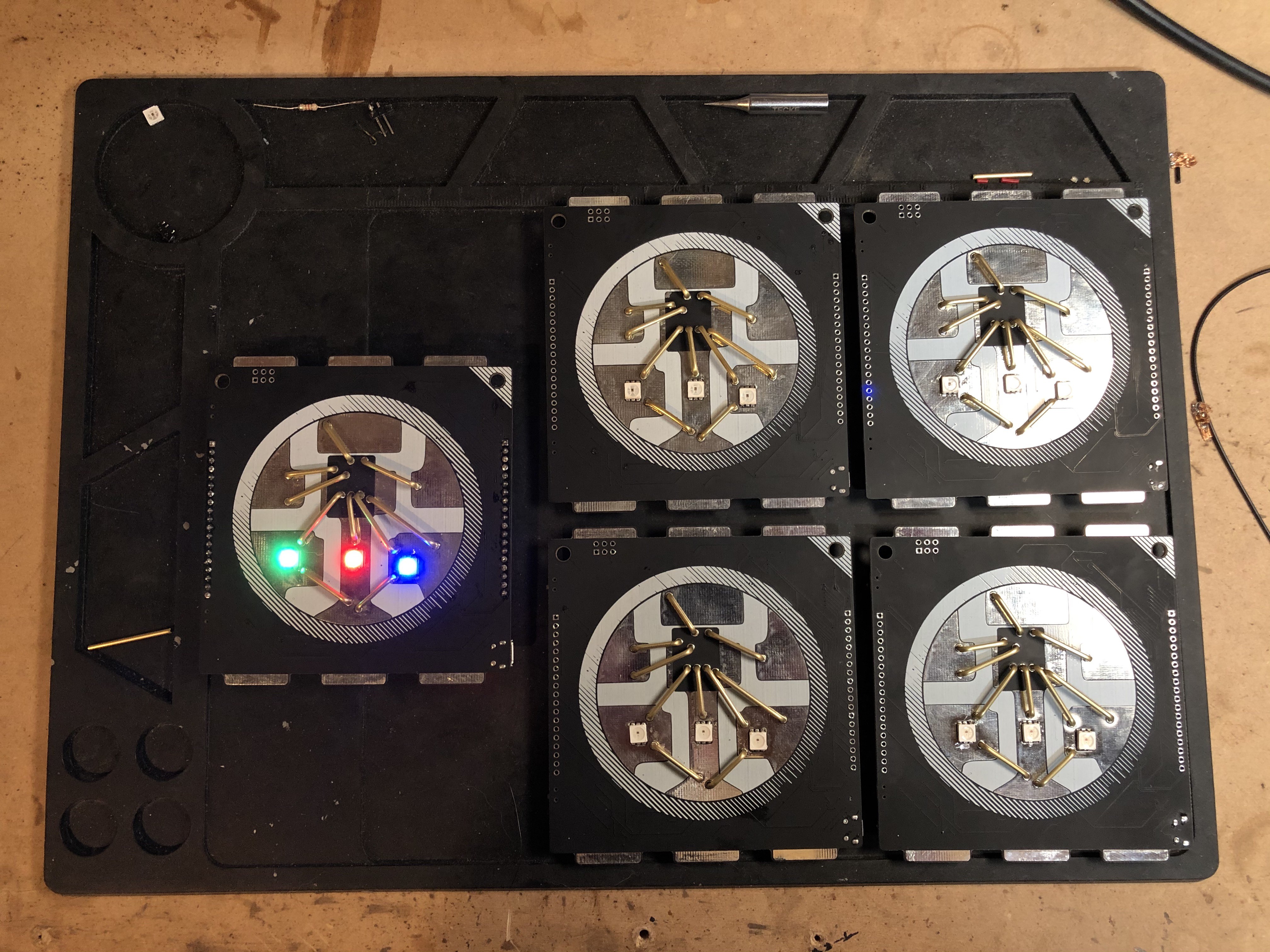
![]()
All 5 v2.2 boards assembled. Streaming / Sharing
I really enjoy watching the twitch streams of others working on electronic projects so I'm trying to start to do that. Here's an archive of a stream I did where I babble about the pixel badge in general for probably too long. Here's a link to my twitch where I'll be streaming more work/progress on these badges and my other projects.
-
Notes on the Brass Tube "Bond Wires"
10/06/2019 at 19:55 • 0 commentsCredit Where Credit is Due
A few months back, maybe even a year ago, I remember seeing these beautiful, delicate, impossible looking electronics projects based around thin brass tubing by Mohit Bhoite. Across his different social media platforms I gathered enough info to try getting creative with the brass rods myself. Please go check out his work, it's very interesting.
What I Used
![]()
Instructions, calipers, pliers, flush cutters, and 1/16" K&S brass tube My first attempt at manipulating the brass tube used these tools.
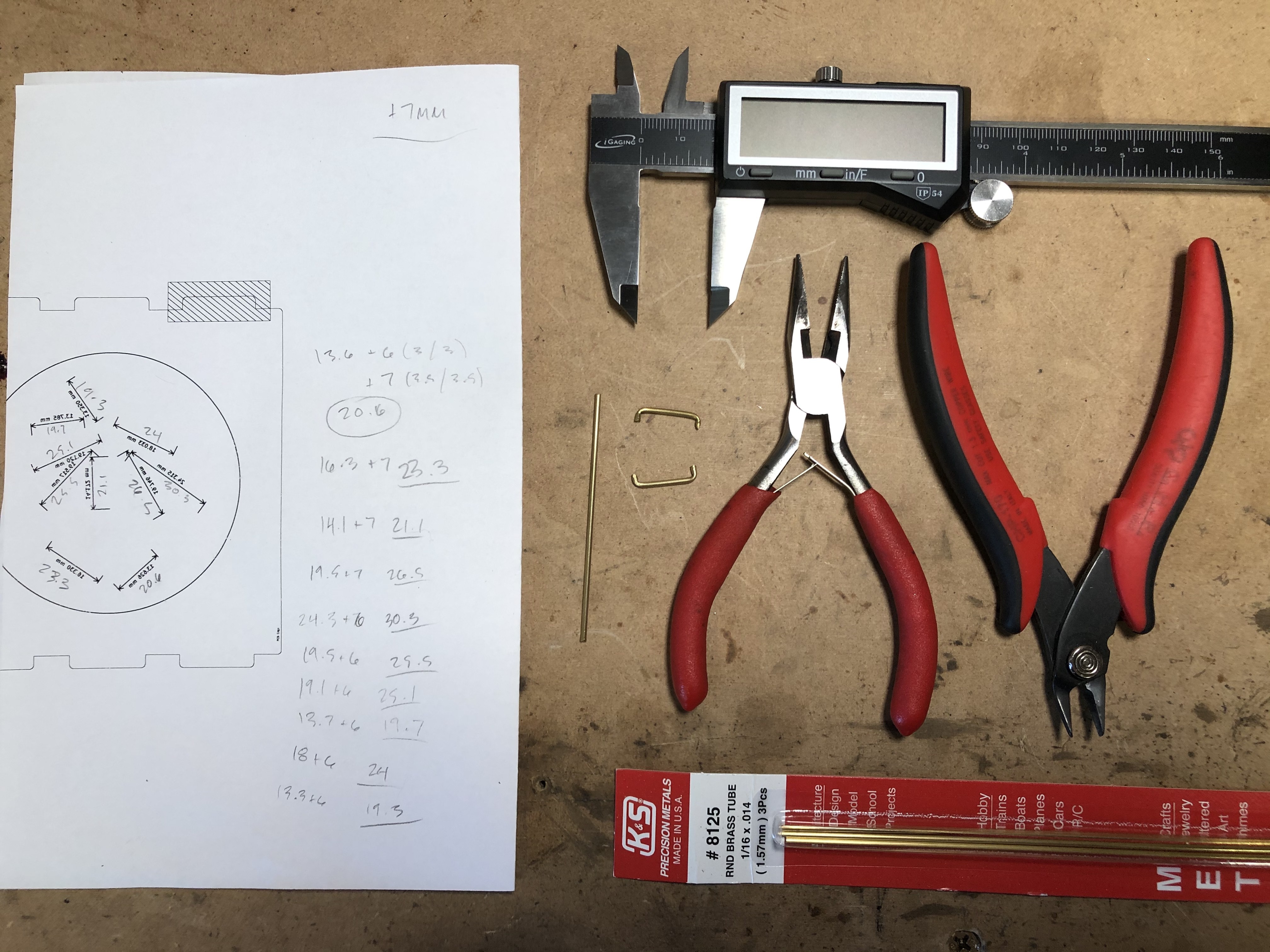
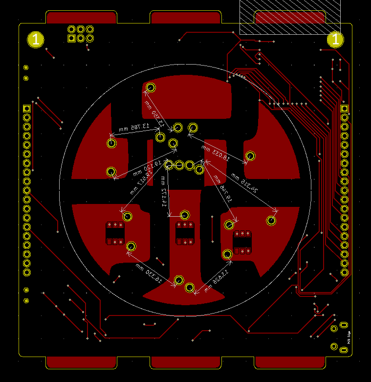
Measuring in KiCad
I used measurements that I had previously made in KiCad to start figuring out how long the brass tubes needed to be for each individual 'bond-wire'. I did this with KiCad's Measurement tool, placing the measurements on the user drawing layer. I then printed out the sheet you see above.
![]()
Measurements made in KiCad Through trial and error I found that I was adding between 6 and 7mm to the distance between the holes on the PCB to get a length of wire with two 90º-ish bends that would be raised up just a little bit above the surface of the PCB.
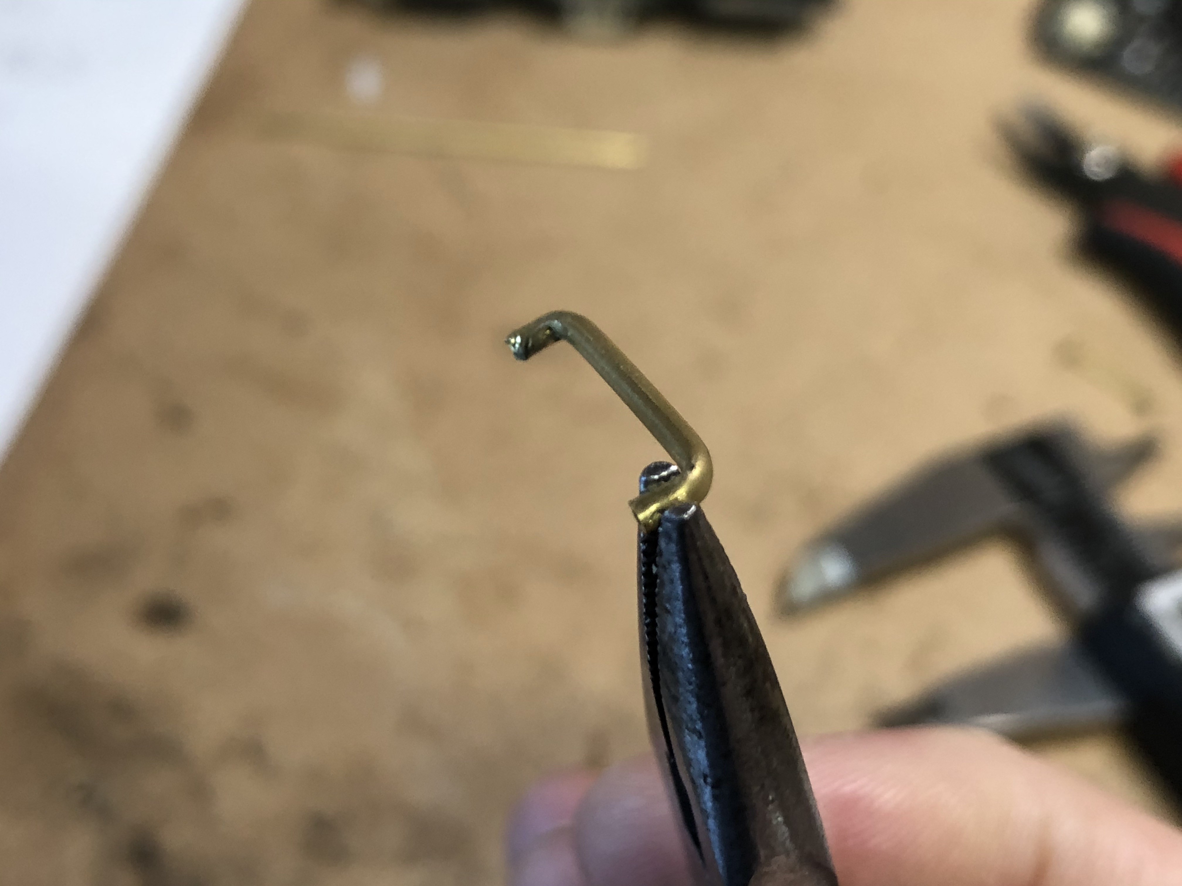
After I figured out how long each of the ten individual (and unique) tubes needed to be, I made a list of lengths, measured and scored each length with the caliper, cut them with my flush cutters, and bent them with the needle nose pliers. I did my best to keep the two bends on the same plane and tweaked them into position as needed. I attempted to use the K&S tubing bender, but it's designed for larger diameter rod/tube and it didn't work any better than my hand and the pliers in my opinion.
![]()
Pre-bent bond-wire Using the flush cutters flattened out the tube where I cut it, so I used the pliers to force the tube back into a tube-like-shape that would place nicely with the round holes they were meant to mate with. I'm being pretty lenient with the tolerances here so I was able to bend any tubes that didn't land perfectly in their holes until everything seated nicely. I also didn't care too much about marring the ends of the brass tubes as they would be nested within the hole in the PCB and I didn't think you'd be able to see many of the imperfections.
![]()
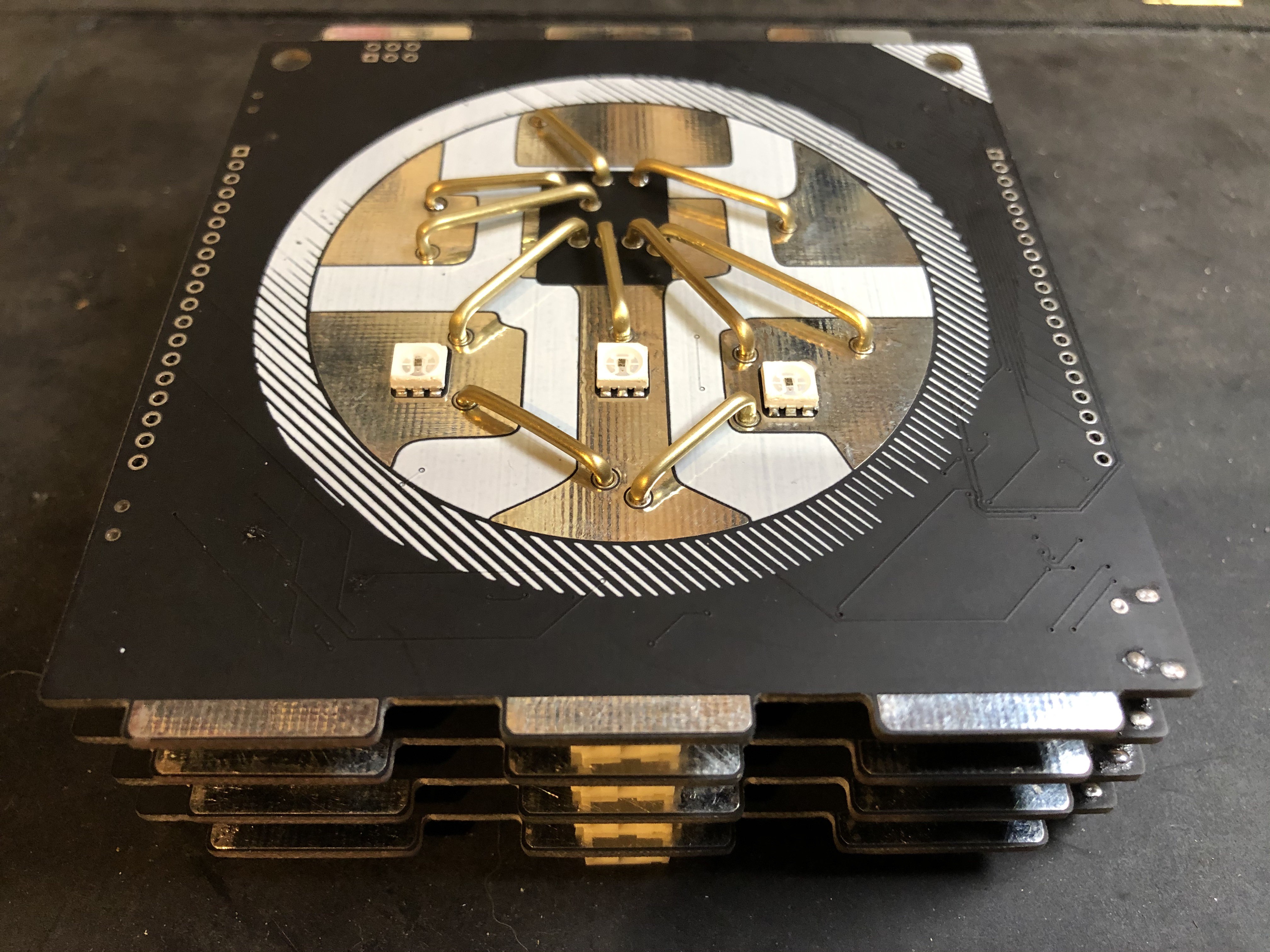
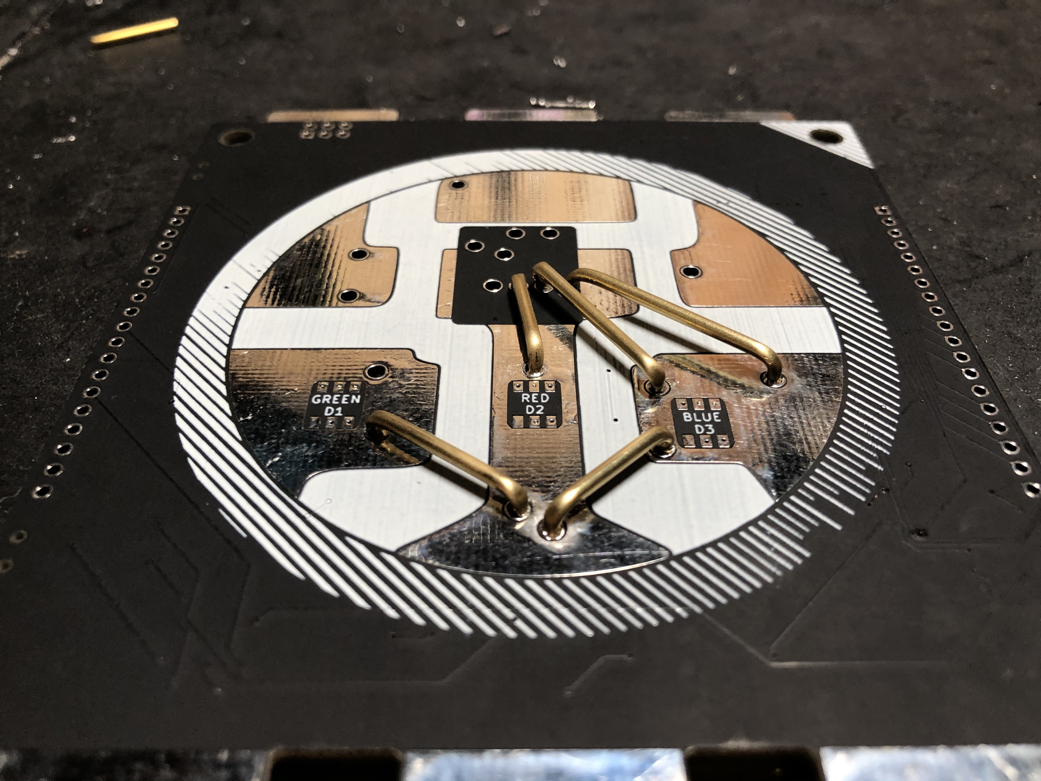
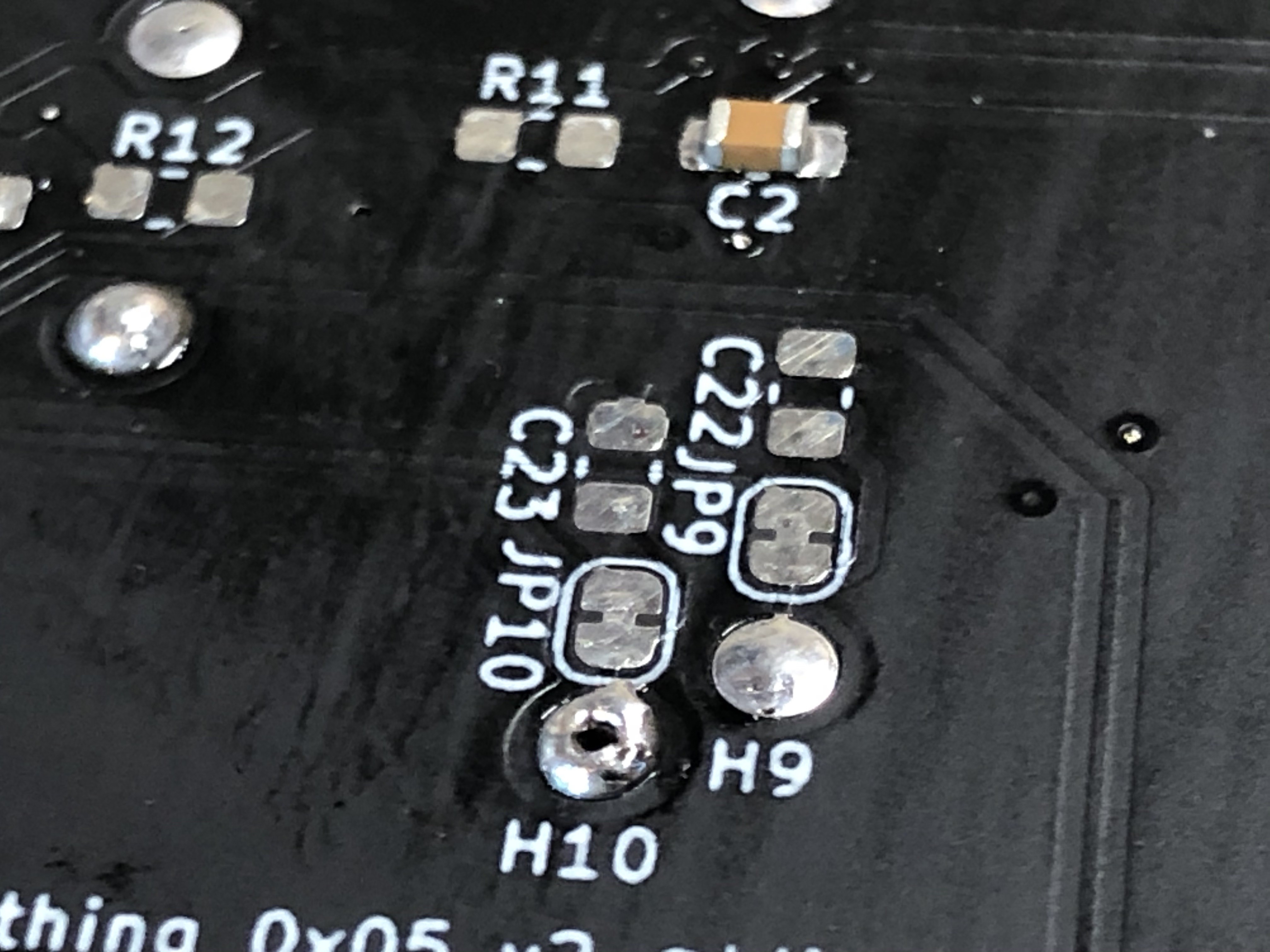
Fairly clean fit/finish I can get a really nice fit my bending the brass into the exact position I want it, and it snuggly fits into the 1.7mm holes in the PCB. The tension of the bent metal was enough to hold the tubes in place while I flipped over the board and soldered them into place. For the most part they all soldered very nicely save for one tube (H10) that was protruding a little bit. I will be mindful of this in the future.
Overall, the front of the PCB looks extremely clean as far as the attachment of the brass tube, especially in comparison to the first version of this board where I essentially welded the tubes to the large copper pads.
![]()
H10 wasn't cut as short or as clean as the rest of the brass tubes Here's a short clip of me the first bit of code I have running on the first prototype. It's a slight modification to the Adafruit Neopixel strandtest example that allows for touch input.
-
Continuation of a Theme
10/06/2019 at 17:46 • 0 commentsPixel Badge 2 : Dark Pixel
![]()
Clockwise from top left. Protoboard, Cardboard v1 and v2, followed by v2.2 and v2.1 of Pixel Badge 2 : Dark Pixel I wasn't finished with this whole pixel pcb idea after Defcon 27 so I'm continuing to develop it.A huge chunk of inspiration for part of this project came from Mohit Bhoite's brass rod electronic sculptures. This is where I began my prototyping. I ordered some brass tube from K&S metals per Mohit's suggestion and attempted to test it's solder-ability and continuity on a protoboard.
Cardboard
After I confirmed that the basic idea would work, I made my first cardboard badge prototype. I was in the middle of reading Adam Savage's "Every Tools a Hammer" and it may have inspired me to work with cardboard before jumping directly into KiCad and ordering PCBs.
I started with an SVG of the shitty pixel SAO I made last year, just blown up in size to around 100mm square. I quickly started to come up with a list of changes I wanted to make to the overall design as well as the size.
After the first cardboard badge, I started to work in KiCad and made a rough design and printed it out 1:1, and pasted it to another piece of cardboard for a second test. This 2nd prototype was used for testing the lengths of brass rod I would need for the bond-wires.
FR-4
I moved on to ordering a PCB prototype after being satisfied with the size of the board and feasibility of including brass tubing. Something new to me on this board was getting custom size holes drilled that would accept the brass tube. The brass tube is 1.5mm in diameter so I used 1.7mm holes in hopes of having enough clearance for an easy but solid fit. I completely screwed this up in KiCad by making the pad on the hole's footprint 1.7mm wide, but the hole that was to be drilled got left at it's default setting. Lesson learned ;)
With the holes not being wide enough to accept the brass pipe, I ended up soldering directly to the face of the PCB with copious amounts of solder. In addition to looking terrible, this reduced the number of unique touch inputs I could play with because some of the brass rods were now sharing an electrical connection via the larger copper pads on the front of the PCB. This was disappointing but I was still able to test some ideas and make some progress so I suppose it was still a success.
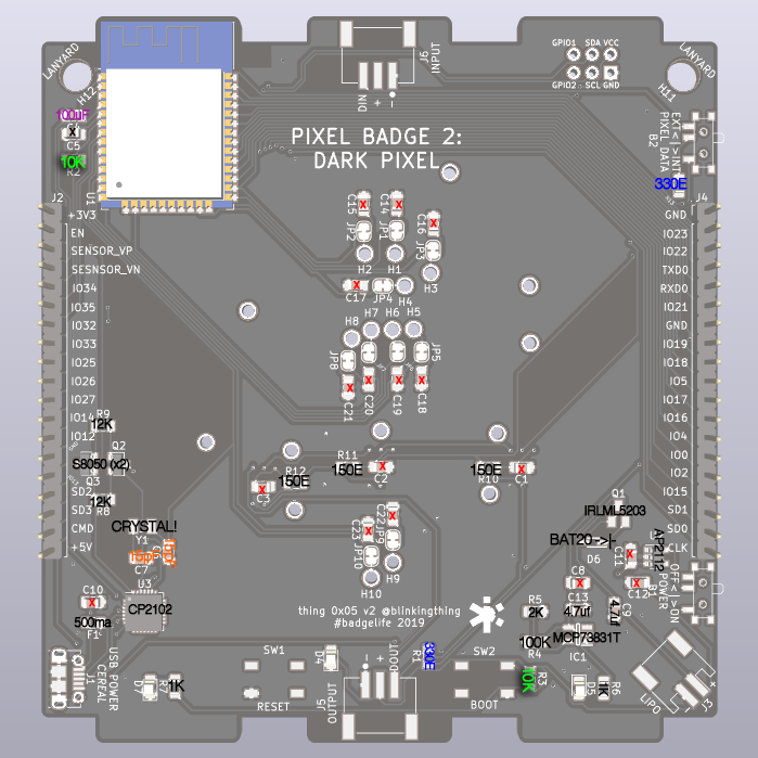
V2.2
I'm now on the 2nd version of the dark pixel board and this time I got the hole drill sizes correct. I've also migrated all the circuitry from the hornbill dev board onto my badge in hopes that I will be able to utilize the lipo charger and USB to UART. I've yet to receive all the components so I haven't been able to fire one up.
That's all for now, the next update will come in about 2 weeks when I get the rest of the parts for v2.2.