 alcor6502
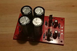
The SuperCapacitor UPS
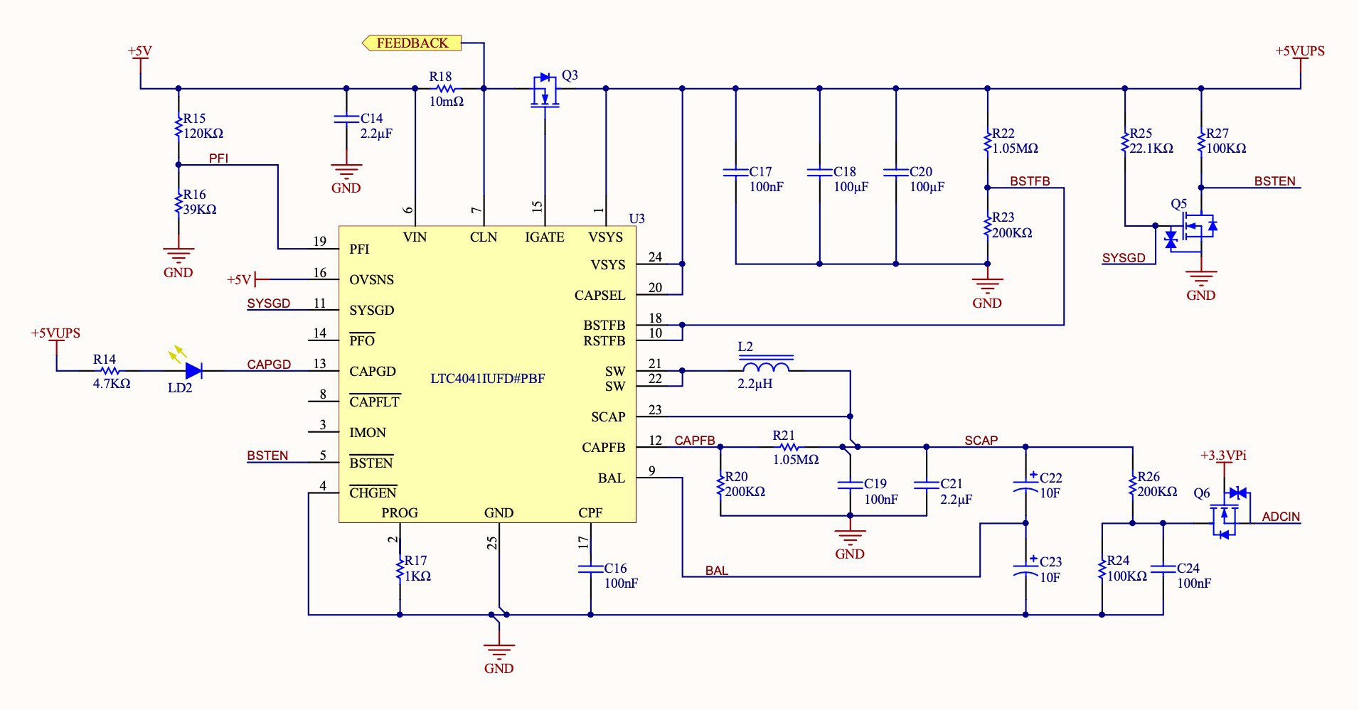
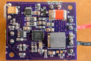
All the UPS functions are performed by the LTC4041, which include a supercapacitor charger and a boost converter, plus all the ancillary circuits to make it a complete solution. The circuit is quite similar to the application note, so I will not spend time describing the inner working of the chip, but only the additions to the standard circuit.
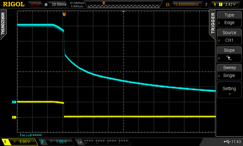
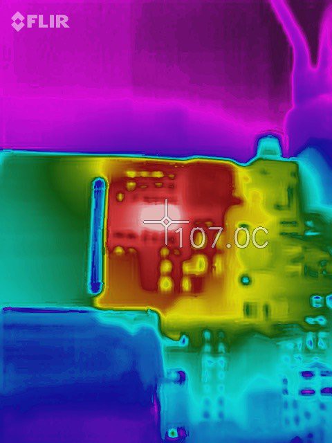
When I developed the prototype, everything was working just fine except in the phase when the capacitors were almost discharged, (below the capture of the power supply output).
This effect was due by the internal power supply of the Raspberry which it disconnects after the input reaches about 4V, but upon disconnected the load seen from the buck converter significantly reduces and subsequently its voltage output rises, enabling again the Rasperry power supply which it would raise the load and trip again.
To avoid this lousy behavior Q5 is used to shut down the LTC4041 boost as soon as the power supply is 7.5% below a value set by the R22 and R23 resistors, which they have a double function: as feedback for the boost converter and as input for the comparator which drives SYSGD.
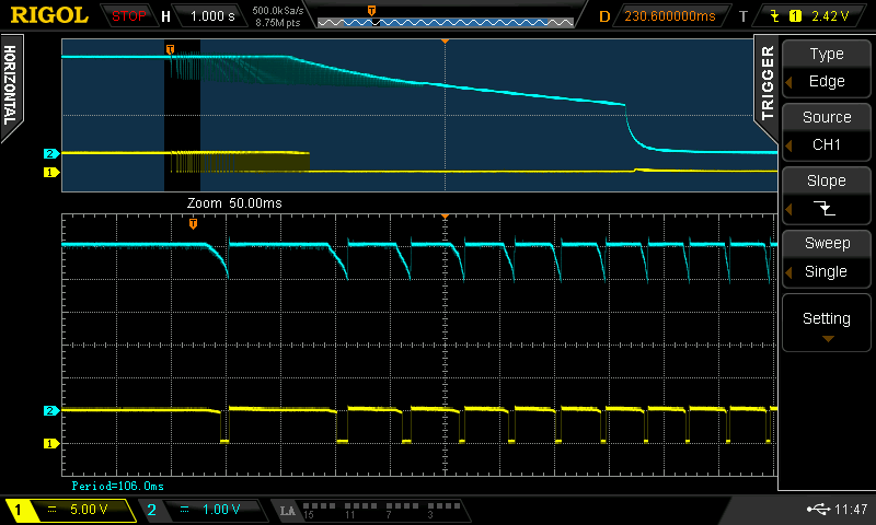
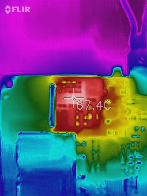
Using the signal SYSGD, you can drive BSTEN, which, when low, disables the boost converter, and, if the voltage of the supercapacitor is below 2.5V, the LTC4041 goes in lookout mode and prevent the boost converter from starting again. (below the power supply behavior with the Q5 working)
I extensively tested the circuit to verify that SYSGD only trips when the supercapacitors are almost discharged, here below the response of pulse load of 2A with a duty cycle of 200ms Off and 5ms On. It sows the difficulties of the boost converter to maintain a stable voltage when the supercapacitor is close to complete discharge.
To reduce the number of unique components, the voltage divider of the supercapacitor charger feedback is the same as R22 and R23. The maximum voltage charge is then set to 5V, to extend the life of the supercapacitor, I recommend the version with 3V working voltage, but you can use any of the three members SCCT20 family, in my prototypes I used the cheapest one without any issue.
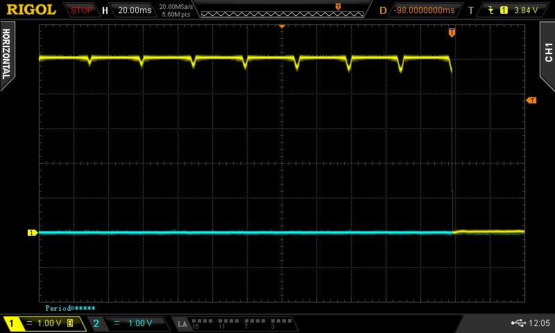
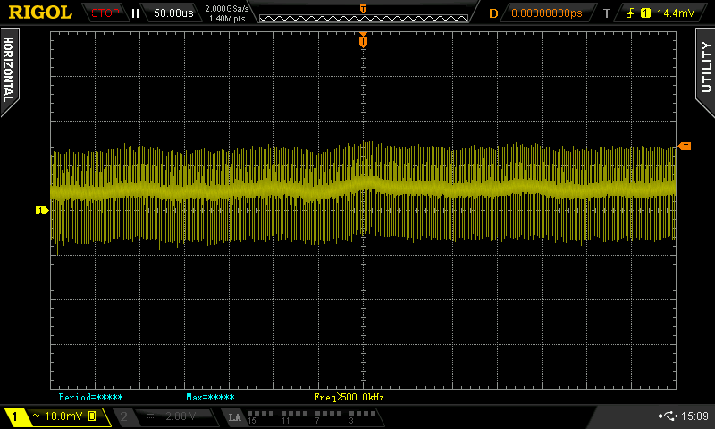
The ripple of the boost converter is quite high, around 100mV with a strange tooth shape waveform which disappears when the supercapacitors are at 3/4 of the charge, this behavior is also present on the development board from Analog Devices used to develop the prototype.
Once the supercapacitors are partially discharged, the ripple settles in this waveform.
Raspberry Power Supply
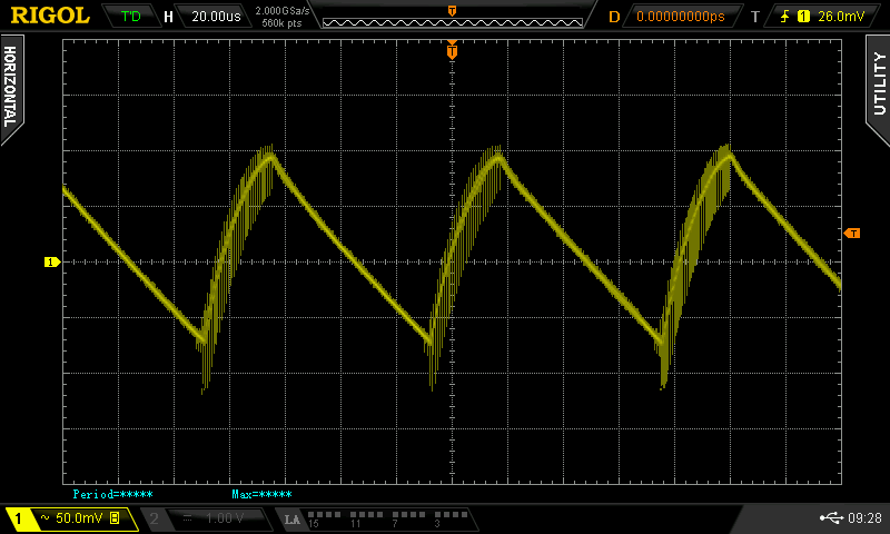
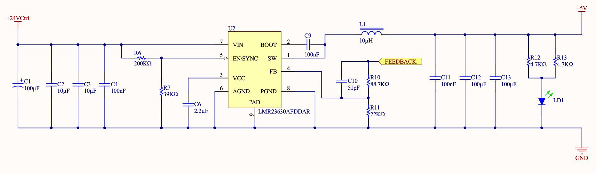
To provide a clean and stable power supply to the Raspberry, I used a Simple Switcher from Texas Instrument. Since the goal is to have a low ripple and clean power supply, I choose to use the chip with the FPWM option.
The output and input capacitors are ceramic to improve transient response, and the component placement follows the datasheet's suggestions. I added a 51pF capacitor to increase the stability of the feedback loop. The feedback point has been taken after the current sense resistor of the UPS to improve voltage stability on high load.
The overall ripple at 2A is about 20mVpp.
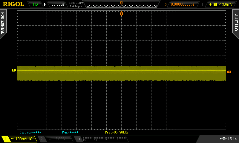
In theory, the power supply can deliver up to 3A, but due to the constraint of the copper available, the maximum load is around 2,5A, the case temperature of chip settles around 110ºC.
To prevent the power supply to work with an input voltage too low, a voltage divider based on R6 and R7 is used to set a minimum start working voltage of 9.5V and a shutoff of 7V.
Soft Latching Power Switch Circuit
The design of the soft latching power switch required quite some time, I search the internet extensively to find a good inspiration, but almost all the circuits were designed for 5V or 12V power supply and adapting them for the required working voltage range (9 to 24V) was often not feasible or impossible. I tried the omnipresent EEVBlog solution, but I wasn't pleased with its performance. Other circuits couldn't work with a large...
Read more »


 Bud Bennett
 Yann Guidon / YGDES
Hi. I need some advise. I assemble it without MC and Pi. Had to play with R15 as my LTC4041 did not work with 1.24V PFI. Made it 1.4V. Caps charged as should be. LD1 ON, LD2 ON until caps fully charged. Have issue with Q5. When power disconnected +5VUPS drops to 0.88v very fast. SYSGD = BSTEN = 0.88v. LD1 and LD2 OFF. Boost is off. Why if it should be enable if BSTEN < 1.2V ? If I short BSTEN to GND and release boost starts (LD2 ON) and keeps desired voltage level until next power cycle. As Q5 I used AO3400 and 2N7002. What I do wrong?