Bud Bennett
-
Noise Analysis
03/06/2024 at 22:50 • 0 commentsI had a PM from someone who built the probe and then wondered why the output noise was so bad. They were measuring about 100mV p-p at the output with the inputs shorted together. At first I had a difficulty believing the noise was that bad, but I got the same result when performing the same measurement. In fact one of my probes was a bit worse than 100mV p-p. So why is it so bad -- I don't know the answer yet, but I can confirm that LTSpice predicts the same result.
To get an answer I ran a .Noise analysis on the entire probe (with parasitics, but that doesn't matter much). LTSpice predicts that total RMS noise voltage at the output is 2.1832mVRMS. I use a fat-finger rule to get p-p from RMS by multiplying the RMS value by 6, so peak-to-peak output noise is about 13.1mV p-p at the scope input, if it is measuring with 1X. If you select the 10X probe setting then the noise will jump to 131mV p-p, which is what I'm seeing.
This doesn't bother me too much because most of what I measure with these probes is repetitive in nature and I can average the noise to a much lower value. But you might have a problem if you need to dig a small, non-repetitive signal out of this noise.
-
Some measurements
02/18/2022 at 21:31 • 0 commentsA fellow maker put the diff probe under test, with some serious equipment: https://electronicprojectsforfun.wordpress.com/a-100mhz-differential-probe-from-hackaday-with-keysight-autoprobe-connectivity/
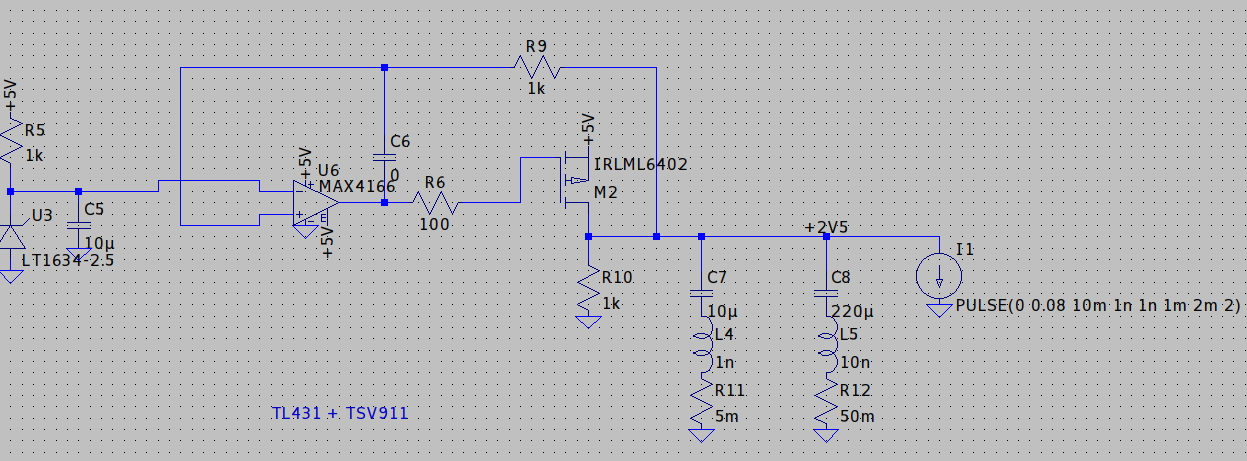
We are now working on a slight change to the offset current injection that won't impact CMRR as much, and an enclosure.
The design that was posted previously (with +/- 2V5 dual supply) requires voltage regulators that are pretty specific, expensive and hard to get, so we're looking into building our own from TL431 references, TLV911 OpAmps, and a pair of FETs. Here's the positive rail:
These parts are comparatively cheap, and replacements should be easy to find. The simulation results are looking promising, and we'll just test it.
A simple dual output DCDC converter can be used to generate the required +/- 5V from a scope's USB output - at least for one probe. Or two, if the DCDC can supply enough current.
-
Addition to the previous log: compensation
09/05/2021 at 18:48 • 0 commentsIn the previous log (https://hackaday.io/project/169390-a-10x-100mhz-differential-probe/log/197059-slim-probe-build-log-and-first-findings) I ranted about having to swap caps to get the input attenuator into the trim cap's range. Here are some more details about that.
In step 2 of the compensation procedure (see here: https://hackaday.io/project/169390-a-10x-100mhz-differential-probe/details far down) we try to match positive signal path's AC gain with DC gain. If they don't match, we get this kind of output error:
![]()
(Ch1: single ended reference input, Ch2: differential probe)
There's an overshoot in the probe's output, which means that the AC gain is too high.
The probe was equipped with
C5...C8 = 330p + 22p + 220p + (2...10)p = 574...582p.
This was too low even with the trim cap at the upper end. The probe peaked to 2.2 V with an actual input of 2V. We can guess the right overall capacitance as
574 * 2.2/2 = 631
which seemed rather high to me, so I swapped the small cap to get
C5...C8 = 330p + 68p + 220p + (2...10)p = 620...628p.
The result:
![]()
Since I got too low AC response now, the 68 pF cap was too large. And, unfortunately, estimating the right cap values from one scope shot apparently isn't an exact science.
I ended up with
330+220+33+10+trim = 595...603 pF
to get this result:
![]()
That was ok and I was also able to match both signal paths.
Swapping these caps was very difficult because the layout doesn't have thermals for the caps' ground connection, which means that the solder joints were very hard to heat up even with low temp solder.
One obvious solution to this would be to increase the trim range, but the temperature coefficient of the JR100 (or JR030) trim caps is lower than that of trim caps with a higher range. We'd be sacrificing performance in the application for convenience in the assembly and compensation, and that doesn't sound like a good compromise for a device that is only built in singles (and caps are cheap).
-
"Slim" probe build log and first findings
08/24/2021 at 20:23 • 1 commentIn the previous project log (https://hackaday.io/project/169390/log/194914-adding-a-more-sophisticated-scope-interface) I described a modified probe that allows to inject an offset current to adjust the probe. Some scopes have an interface that has additional connections to supply active probes, communicate with them and adjust them, and we're trying to make this probe compatible with that interface - at least the analog and supply part (communication will be added too, but closer to the scope connector).
While Bud was already pointing out some shortcomings of the modified schematic, namely gain error and lower CMRR, I had already ordered PCBs from aisler and assembled one once they arrived:
![]()
My plan was to assemble one even if it's not perfect, send it to another tinkerer who has the necessary equipment to test it thoroughly, and use his and Bud's feedback to adjust the next revision of the schematic, the layout and also the overall shape (for a 3D printed enclosure).
Note:
1) I didn't place protection diodes
2) The layout didn't contain spark gaps and their ground trace
3) an extra cap had to be added to the attenuator to compensate the probe. We'll get to that later.
Assembly was done with low temp solder (see here for the details about how I solder small/low temp stuff: https://hackaday.io/page/10792). However, swapping out caps was still tedious and time consuming because it's an iterative process.
Caps, Caps, Caps
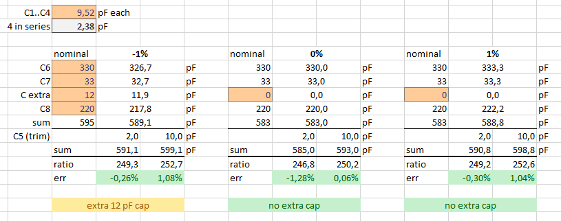
I had previously built a probe as per Bud's original design and knew that the effective capacitance of C1...C4 is significantly lower than 2.5 pF (4x 10 pF caps in series). On his layout, the effective capacitance was around 2.31 pF (4x 9.25 pF in series), so C6...C8 had to be around 572 pF (+trim cap 2...10 pF) to get a 1:250 attenuator.
On my layout, the capacitance of C6...C8 had to be 593 pF (330 + 220 + 33 + 10 pF), which is significantly higher than on Bud's layout. We came to the conclusion that it's most probably the absence of the spark gaps and their ground trace that leads to this significant change in parasitic capacitance (obviously, this is something that can be found out by comparing with a layout with a ground trace). The trim caps were at 1/3 and 2/3 of their range. I created a spreadsheet to calculate a probable range of the capacitance of C1...C4, taking into account the tolerance of C6...C8:
At the bottom, the spreadsheet calculates the resulting attenuation given the values for C1...C4 and C6...C8 (+trim). Since both trimmers were somewhere around their center, I wanted the resulting error at both ends of the trim range to be somewhat symmetric around zero (highlighted in green).
The left block shows the result for the case that C6...C8 were at their lower end (-1 %). To get into the right trim range, C1...C4 had to be set to 9.52 pF (top left). Similar for the center and right block.
Next step was to select a set of capacitor values that allow to build a probe where
- the "base" capacitance is known to be not too large for the lower end of C1...C4 and +1 % in C6...C8 (that's the one extreme of the overall spectrum)
- a maximum of 2 additional caps with known values can be added to get into the right trim range even for the upper end of C1...C4 and -1 % in C6...C8 (the other extreme) and all other combinations
- so no cap would have to be swapped - we'd just add more and know that it'll be good.
Some experimentation with the values made it obvious that these goals can't be achieved with just 3 footprints, so I added a fourth footprint to the next schematic and layout revision.
Good cap combo using values from the E12 series
The base values are 560 + 18 pF, and one or two 12 pF caps can be added.
For the low value of 9.52 pF for C1...C4:
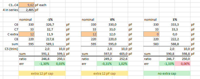
For the center value (9.62 pF):
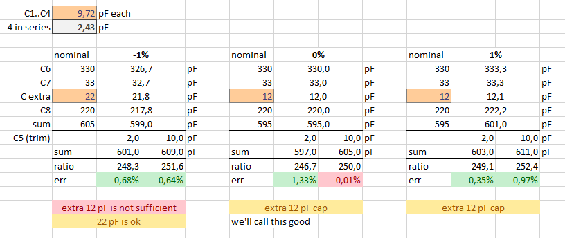
for the upper value (9.72 pF):
So during the compensation procedure I could start with just 560+18 pF, and add one or two 12 pF caps until the trim caps can do their job correctly.
Good cap combo using values from the E6 series
Bud pointed out that he only uses E6 values. Well, since their spacing is wider, it's a bit harder to cover all cases. Starting with 330 + 220 + 33 pF, we can get very close and only one extreme case needs extra work if an extra 12 pF (yeah, that's E12 again...) isn't sufficient.
For the low value of 9.52 pF for C1...C4:
For the center value (9.62 pF):
for the upper value (9.72 pF):
So only if C1...C4 have high capacitance and C6...C8 are low, we need more than 12 pF to get into the right range.
Aaaand given that the new layout will probably come with its own little intricacies, all this was probably pointless. But it was fun to bloat just one sample to this mass of numbers!
Next steps are
- wait for feedback on the current design's performance
- implement it
- order, build, test again.
(Attach current schematic - not built yet)
-
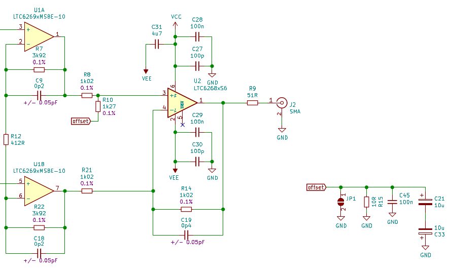
Adding a more sophisticated scope interface
07/02/2021 at 18:20 • 2 commentsThe probe as it was designed by Bud and Paul works well and does the job. However, as always, there are ways to make it do more: Wolfgang was looking for a modified version that can connect to his keysight scope and make use of the scope's AutoProbe interface. Keysight scopes have an extra interface (a row of pogo pads below the BNC connector) that provides an I2C interface and supplies various voltages and an adjustable offset current to the probe. This can be used to supply the probe, auto-detect it, and set the offset. That's all pretty neat, but requires a couple of modifications on the probe and an external adapter that connects to the scope. The interface is described here:
I found this quite interesting and started a design that can be used with or with the AutoProbe interface. I also wanted a more "pen"-shaped probe and Wolfgang suggested adding a white LED to the tip. Other modifications (starting off with Bud's 5V design):
- The spark gaps had to go, because they add extra input capacitance
- wider gap between the tip pads
- not a layout modification, but the clamping diodes D1 and D2 also add some capacitance that is not desired. They are not populated for initial performance measurements.
The modified probe needs a different external power supply if used without the AutoProbe interface, but that's not too hard to accomplish. It can now even be a simple 2S LiIon or LiPo battery, or a DCDC converter with +/- 5V output (those black blocky things)
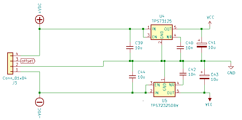
Power supply
Power supply comes either as +/-12 V or as +/-3...6 V from the AutoProbe interface (some scopes apparently have +/-5 V only). This requires a different power supply on the probe. Instead of creating a virtual ground from a floating 5V suppky, we now have to create +/- 2V5 from the fixed dual supply with fixed ground. So I replaced the OpAmp that creates virtual ground by two low noise linear regulstor (TPS73125 and TPS72325).
This part of the schematic also shows that the probe is connected to the AutoProbe adapter with a 4-pin connector.
Offset injection
The AutoProbe interface can inject an adjustable offset current limited to +/- 1 mA and a low voltage (5 V? not sure). This is sent through a 10R resistor at the bottom of R10 (instead of wiring R10 to ground). A 100 nF cap and a pair of tantalum caps were also added:
This allows the offset to be adjusted by +/- 1 mA * 10R = +/- 10 mV. That's just our first guess, and the offset resistor is large enough for comfortable rework (1206). It can also be left out and placed externally for experimentation.
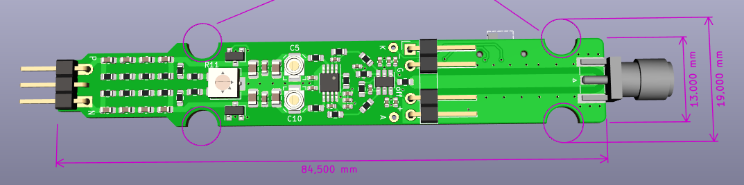
Layout
Here's the new slim layout:
(84.5 mm x 13 mm)
The input header is a 3-pin header with the center pin removed, I was too lazy to modify the 3D model accordingly. Same for the 4-pin connector which can be a 5-pin type with the center pin removed. In this case I substituted for 2 2-pin 3D models because the 5-pin model would have obstructed the view of the output resistor that feeds the waveguide.
LED
The actual LED is not on the PCB, because that would have interfered with the attenuator layout. It's connected to a pair of through-hole pads (labeled "A" and "K") right next to the 4-pin connector instead, so it can be connected from either side of the PCB, depending on what would better fit the enclosure. There's a little switch in the back to turn it on and off.
SMA connector
The SMA connector is a bit smaller (6.35 mm wide) than the one on the initial layout (9.5 mm). It's also further away from the output OpAmp, so we added the waveguide you can see above
Other modifications
R8 and R21 were rotated by 45° to make the overall layout a bit prettier. Looks like a spider now.
The voltage regulators are on the bottom:
There are cutouts for threaded inserts in a 3D-printed enclosure. The threaded inserts on the input end would be a couple mm away from the attenuator, so hopefully they won't interfere with the measurement. On the other hand I'm not sure if a totally different enclosure concept might be better, but we'll figure that out.
Since this layout is new, I'll have to go through all the trial and error of finding the correct capacitors for the input attenuator again. The deviation from the theoretical values that Bud discovered is quite significant.
I also don't know if the ground layout is good enough, we'll have to measure the probe's performance to see what we have to improve, and how.
Design files will be published when we have assembled and tested one.
-
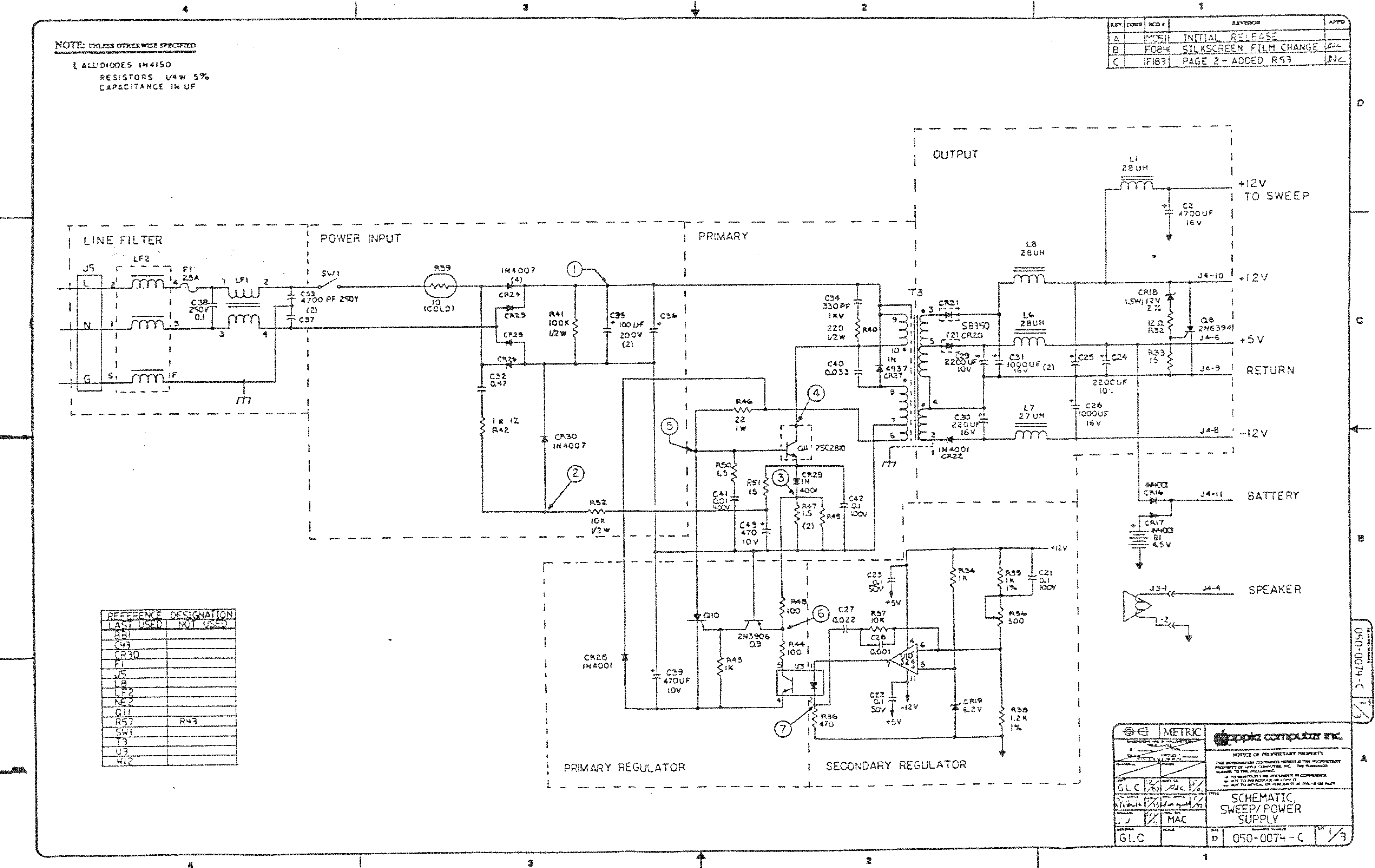
Acid Test
02/26/2020 at 21:24 • 0 commentsI wanted to see how well this probe would perform in its intended application. I took the case off my old Macintosh 512k and measured a few waveforms. Here's the power supply schematic:
![]()
The primary side of this SMPS power supply is not isolated from the 125VAC mains. All of the circuitry to the left of the multi-tapped transformer are moving up and down 180V at 60Hz with respect to the ground reference on the right side. There are a lot of voltage swings that exceed the probe's ability (±25V), but you can get a pretty good idea about what is going on by measuring lower voltages. The first point that I measured was from node "5", the base of Q11, to the virtual ground at the base of Q9. It looks pretty much as it should.
![]()
Then I put the probe leads from node "3" to the virtual ground. Again, as expected.
![]()
The last node that I probed was the gate of Q10 w.r.t the virtual ground. This is a lot uglier, but seems appropriate.
![]()
There is an artifact from the large common mode voltage. I recorded this to show the amount of bleed through from the common mode:
![]()
It is the same signal at the gate of Q10, but the baseline voltage shows the 60Hz common mode. It's on the order of 5mV (50mV @ 10X), so it is tolerable for this situation.
I'm pretty happy at this point. I wish that I had this capability when I was trying to figure out what was wrong with this circuit a few months ago.
-
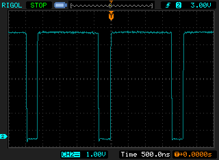
Test Results Using SMA to BNC pigtail
02/25/2020 at 16:22 • 5 commentsMy SMA connectors that I ordered from AliExpress have not arrived, so I ordered two SMA connectors from Digikey for $3.44 each, along with the resistors to correct the gain error in the first gain stage. I am using a 20 inch long SMA to BNC pigtail to connect the probe to the scope input. The power is provided by an old wall adapter that I modified some time ago to output 5.25VDC. The extra 0.25V allows the differential inputs to swing past ±25V before the amplifiers saturate.
Here's a few waveforms showing performance at lower frequencies:
![]()
Channel #1 is the diff probe and channel #2 is the 10X scope probe. Both are connected to the scope's 3V calibration signal.
![]()
This is a 25V 1kHz square wave. Same channel inputs as above.
![]()
A zoom in on the rising edge of the 25V square wave. The diff probe captures the same waveform features as the 10X scope probe.
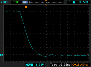
Faster Rise/Fall times:
I don't have a laboratory grade signal source to test the probe, so again I'm using a switching step-down converter to obtain ~10ns transition times.
![]()
This is what the 10X scope probe produces on channel 2 when connected to the inductor.
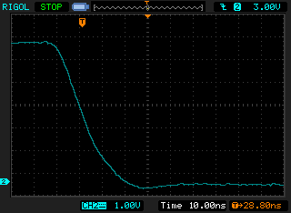
![]()
The above is what the diff probe thinks the inductor waveform looks like.
![]()
This is the falling edge measured with the 10X scope probe.
![]()
The falling edge measured by the diff probe.
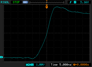
![]()
The rising edge measured by the 10X scope probe. This edge is faster -- about 10ns -- there is ringing from the probe.
![]()
The rising edge measured by the diff probe.
I can't say for sure which probe is telling the truth about the waveforms. My equipment is not up to the task of properly evaluating the performance of the differential probe. But it is good enough for my purposes at this time.
-
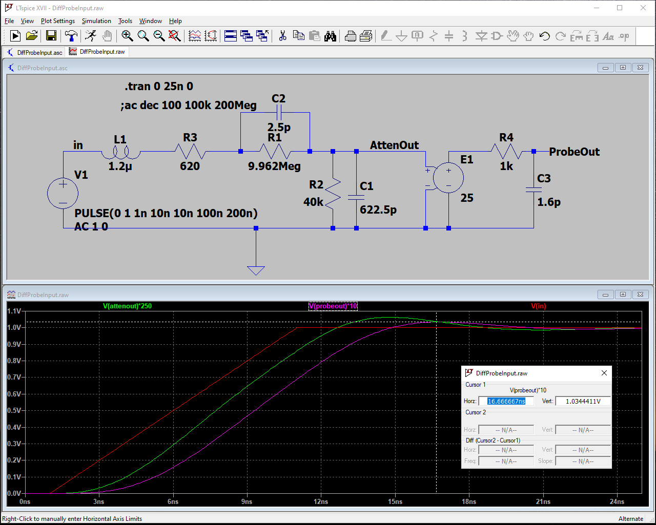
Custom Leads
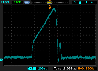
02/12/2020 at 16:54 • 0 commentsThe inductance of a 3 inch long 26AWG wire is 1.23µH. It plays havoc with the diff probe if not properly accounted for. I ginned up a simple circuit to help me visualize how to dampen the ring associated with the lead:
![]() A small value of series resistance in the lead will remove most of the ringing caused by the lead inductance. The largest value of series resistance that can be inserted into a 3 inch long lead is 620Ω. Any more than that will reduce the bandwidth of the differential probe. There is also a small, 0.006%, reduction in gain.
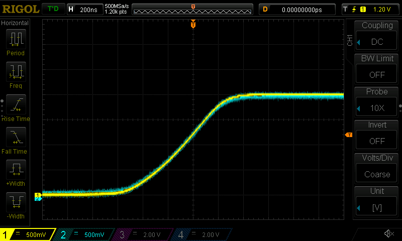
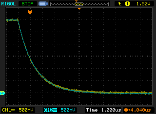
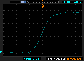
A small value of series resistance in the lead will remove most of the ringing caused by the lead inductance. The largest value of series resistance that can be inserted into a 3 inch long lead is 620Ω. Any more than that will reduce the bandwidth of the differential probe. There is also a small, 0.006%, reduction in gain.With 620Ω, the response to a 1V input step with a 3.5ns risetime is:
![]() There is a 10% overshoot in the probe's response to this fast step. Clearly, if you need fidelity on signals with very fast rising edges the lead length must be as small as possible. But if the rise time is reduced to 10ns the overshoot decreases to only 3.5%:
There is a 10% overshoot in the probe's response to this fast step. Clearly, if you need fidelity on signals with very fast rising edges the lead length must be as small as possible. But if the rise time is reduced to 10ns the overshoot decreases to only 3.5%:![]()
I'll be making couple of sets of custom leads, with unique values of series resistance. There is no need to add any resistance to the PCB. The lead set to use will depend upon the characteristics of the signal to measure.
-
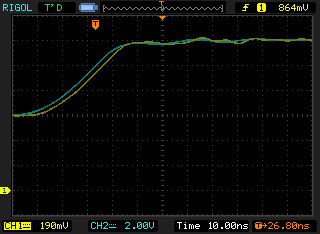
Ringing & Swinging
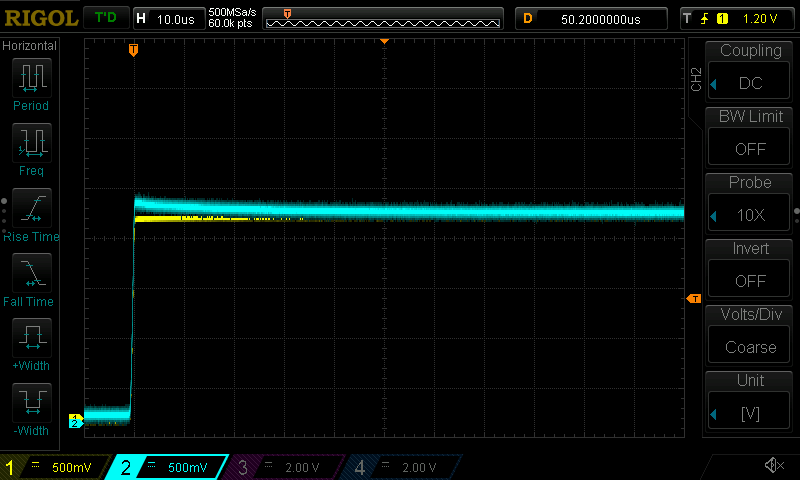
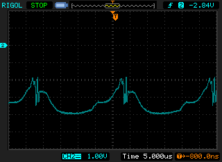
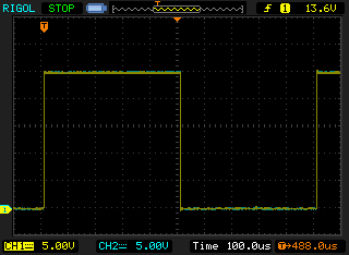
02/11/2020 at 23:10 • 0 commentsI can’t leave well enough alone. I still don’t have the SMA connectors to allow direct connection of the probe to the scope input, but I wanted to evaluate the probe in some more real world environments. I thought that a good test was to connect the diff probe to the gate drives of my T16 battery charger. These signals are 5-6V transitions with expected rise/fall times on the order of 10ns. In order to capture all of the information, you must have 35-70MHz of bandwidth. I have seen, and dealt with, quite a few buck converter gate drive issues over the years.
The top gate drive of the buck converter has a slower rise/fall time than the bottom gate drive. This is usually due to the top FET having a bit more total charge, Qt, because the top FET is a PCh FET vs. the NCh bottom FET. I connected the diff probe positive lead to the top gate signal and the negative lead to the GND of the battery charger. This is what was output from the diff probe:
![]()
The yellow trace is the output of the diff probe, measured by CH1 of my scope. The blue trace is Ch2 of the scope measured with the 10x scope probe. This waveform doesn’t show much ringing associated with inductive parasitics. That could be because of the slower, 40ns, rise time or the care that I took with the PCB layout :).
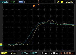
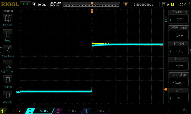
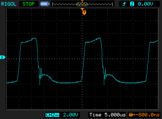
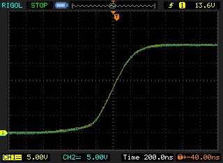
I then connected the probe across the bottom gate signal. This signal is much faster, 5ns rise/fall, than the top gate.
![]()
There is quite a bit of ringing. The ringing can be a result of many things: poor probe grounding, marginal stability of the diff probe amplifiers, unknown bad stuff? Usually, when confronted with unexpected circuit performance I tend to go back to the simulator and see if I can reproduce the effect and get a handled on the problem. I was looking for something that affected the second gain stage, or all gain stages, that would present as shown. I found two things: R23 & R24 had an effect on the ringing due to a fast rise/fall event, and the lead inductance that I was using should have caused ringing when the lead inductance interacted with the input capacitance of the attenuator. Or perhaps it was both, or something else?
In simulation, I found that the first stage amplifier ringing reduced when R23 & R24 were raised above 1kΩ. This damped oscillation was not present in the simulation until the stimulus had some common mode component. And this ringing was quite high in frequency and did not pass through to the probe output.
I also found that the longish leads that I was using to connect the diff prove to the Buck converter may be causing a problem. A 12 inch long 26 AWG wire has a self inductance of around 5µH. If you combine that inductance with the ~2.5pF input capacitance of the probe it will tend to ring at a frequency around 50MHz. If there is no resistance to dampen the Q of the input LC then the ring can be pronounced. A small amount of resistance in series with the probe inputs could remove most of the ringing at the input by reducing the Q of the LC circuit. If too much resistance is added to the diff probe inputs then the bandwidth would be compromised.
I added 470Ω to each of the diff probe's inputs, using leaded metal film resistors. I did not see a significant reduction in the ringing. So what's really happening?
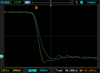
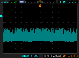
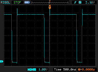
I turns out that channel #1 of my Rigol 1102 appears to ring a lot more than channel #2. At this point I don't know which channel is bad, but my money is on channel #1. When I connected both channels of my Rigol scope to the diff probe output I obtained these results:
![]()
![]()
My Rigol scope has a problem with ringing on Channel #1. I think the diff probe performance is acceptable. [Caveat: I haven't directly connected the diff probe to the scope yet.]
-
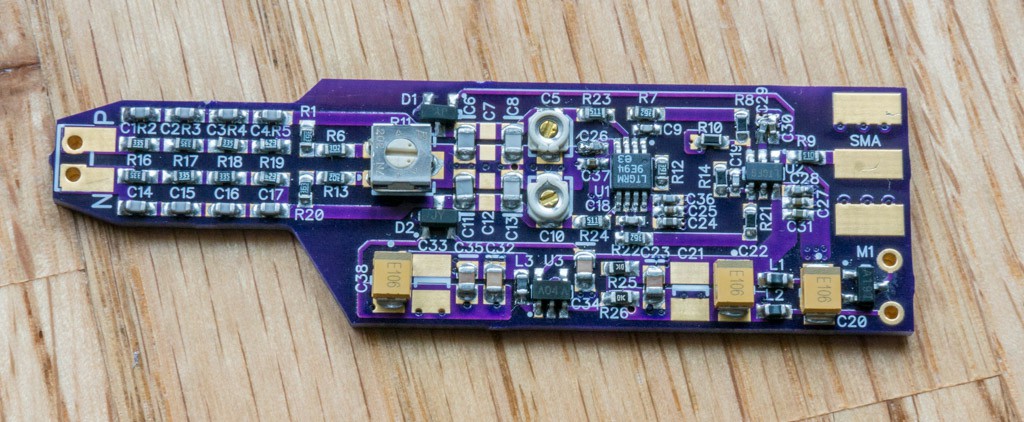
Results from First Prototypes
02/09/2020 at 21:49 • 0 comments![]()
PCBs and components arrived within a day of each other. I had the first prototype assembled and working in an afternoon, with some compromises: I used 3.6kΩ/390Ω resistors for the first gain stage instead of 3.92kΩ/412Ω, and I don’t have any SMA connectors yet, so I can’t tie the output directly to the scope input. So the gain is 3% low.
Power supply current = 52mA.
First thing I checked was the ground supply to make sure that the M7301 opamp was not oscillating — no buzz. I did not populate the 22µF ceramics at the input and output of the LM7301, and I made sure to use 10µF tantalum capacitors with an ESR spec of 2.5Ω to damp any potential ringing at 100kHz.
Next, I tied the inputs together and connected a scope probe to the output. No buzz there either...I’m breathing a bit easier now. I measure the output offset voltage to be -18mV. This seems a bit high (low, really) to me, but it is within the envelope of the amplifier’s Vos x Gain. The easiest way to see a trace is to connect the probe inputs across the scope’s square wave calibration output. The output is 386mVp-p for an input of 3.96Vp-p — 0.0969V/V. The lower gain is expected because of the temporary resistors installed.
But something is not right. The probe output is showing a pronounced rounded edge instead of a sharp square edge. Adjusting the trimmer capacitor in the positive signal path has a negligible effect. I can calculate the probe’s AC gain from the difference between the input and output waveforms — it’s about 7.3% too low. I remove the 15pF 0603 capacitor in the attenuator. This helps, but the AC gain is still 5% too low, so I replace one of the 300pF capacitors with a 270pF 1%/0805. Now the DC and AC gains almost match perfectly and I can use the pot and the trimmer capacitors to fine tune the probe. [This is a strange result for me. I bought 10pF±1% NP0 capacitors for the attenuator, but they appear to be 7.5% low after assembly onto the PCB. I believe this is the first time in my life that capacitance is lower than expected!]
At this point I decided to build a second prototype, with the same component values now in place in the first one, to see if there was some big error somewhere. The second prototype performs nearly identically with the first, except the output offset voltage is only -11mV. In a way this is a good thing...consistency is good.
Let’s measure CMRR:
I believed the simplest way to measure low frequency CMRR was to connect both probe inputs to a 125VAC signal and see what the output did. It was not very pretty:
![]()
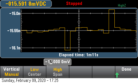
It’s not really bad — about -90dB — but I was expecting a better result. Maybe I had not calibrated the CMR and AC gain correctly. So I connected both inputs to a 30VDC supply and rotated the potentiometer to cancel the DC CMR error while looking at the outputs with a DVM. I got the DC CMRR to better than 100dB. Here’s a screen dump of the HP DVM showing the DC output voltage of the probe changing with the the applied 30VDC CM input. Each large spike is me turning off/on the 30V supply. The only thing that's important is the deviation between the large spikes. It’s 0.25mV! That’s more like what I was expecting.
![]()
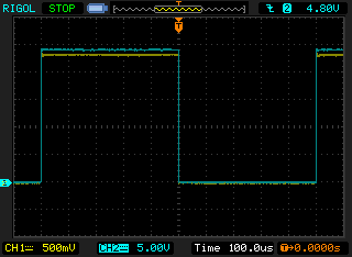
I set up a test circuit to provide a 1kHz 30Vp-p square wave (a more controlled waveform than the mains input) to test the CMRR. This was just a 2N7000 FET with a 3.3kΩ load resistor connected to a 30V supply, with the 2N7000 gate driven by the 3V scope calibration output waveform. Rise/fall times improved from ~1µs to ~100ns. I was able to calibrate out the DC and AC common-mode contributions to where the probe output looked like this to a 1kHz +30V CM square wave:
![]()
Ch2 shows the 30V square wave. I would call this less than ±1mV p-p variation. That’s > 83dB CMRR at 1kHz.
Unfortunately, I don’t have any appropriate equipment to thoroughly test the differential probe performance beyond this point, unless I get access to better lab equipment. I’ll have more/better data after the SMA connectors arrive and I can directly connect the probe to the scope input. But here's a scope trace that might anticipate the result:
![]()
A 10X 100MHz Differential Probe
A DIY oscilloscope probe to dig small differential signals embedded in high common mode voltages.
 A small value of series resistance in the lead will remove most of the ringing caused by the lead inductance. The largest value of series resistance that can be inserted into a 3 inch long lead is 620Ω. Any more than that will reduce the bandwidth of the differential probe. There is also a small, 0.006%, reduction in gain.
 There is a 10% overshoot in the probe's response to this fast step. Clearly, if you need fidelity on signals with very fast rising edges the lead length must be as small as possible. But if the rise time is reduced to 10ns the overshoot decreases to only 3.5%: