 Josh Kittle
With lessons learned from Rev 1, design changes were made and the Rev 2 PCB order went off to the board house. This order was placed on Dec 10, 2019. Shown below is the Rev 2 PCB design.
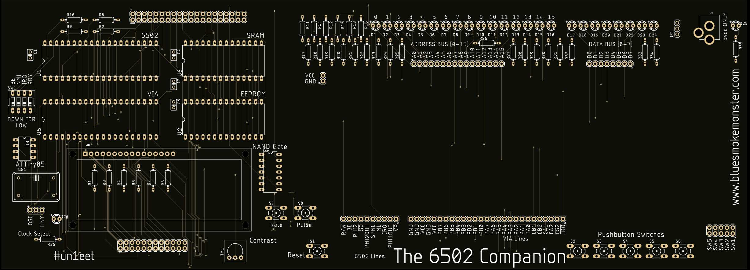
In this revision, the power jack was wired properly, I added a bunch of different LEDs to show the state of the address and data bus lines. I added DIP switches to allow for manipulation of certain key 6502 signaling line states. I also played with layout a little bit. Shown here is a testing sample of this run. Only 5 of these PCBs were made.
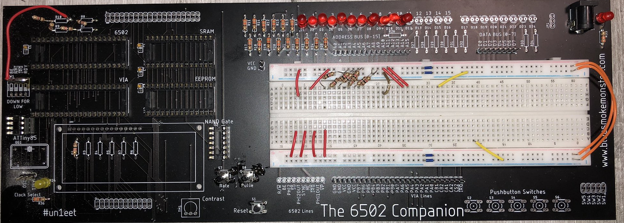
I didn't have the smaller 3mm LEDs yet, so I made do with some 5mm LEDs that I had on the bench. More lessons learned, more bodges, and we were on to Revision 3.
Discussions
Become a Hackaday.io Member
Create an account to leave a comment. Already have an account? Log In.