Time for another update. Mind you, at this point I am not documenting work that was already done in the past, but am following my actual development in real time. Therefore updates will be spaced much further apart, depending on how much time I can devote top this project.
After finishing the adress-datapath design, it is time for the data-datapath.
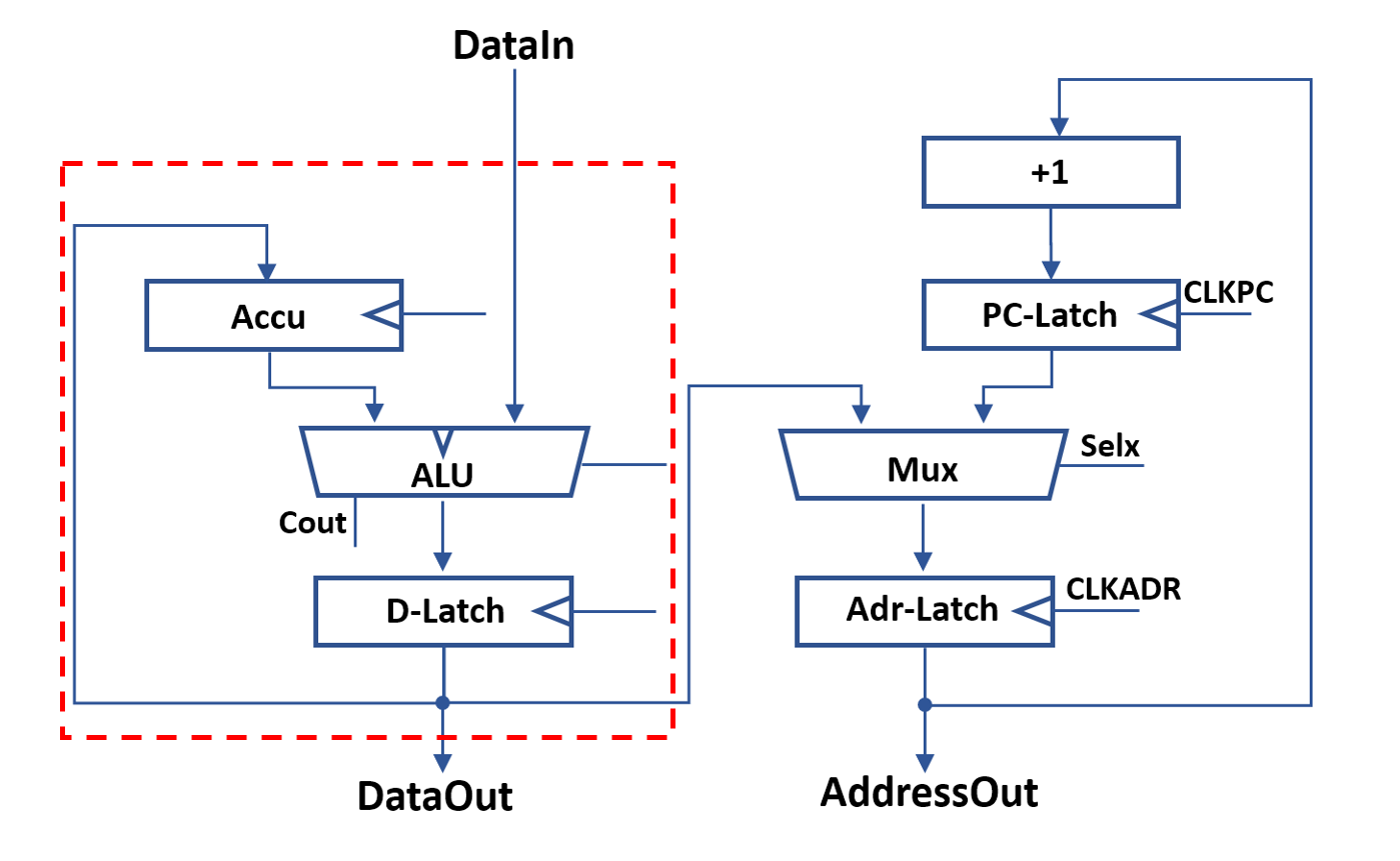
The data-dapath encompasses the left side of the system design. The original M-CPU ALU was rather simple and only supported the two operations that were needed directly by the ISA: (Y,Cout)=A + B, Y=A NOR B.
However, I changed the datapath a little to allow use of latches in the design. As a consequence, all reads are directed through the ALU. Storing the accumulator to memory also requires data to pass throught the ALU. Therefore, in addition to the operations above, also Y=A and Y=B have to be supported. When looking at the detailed logic, this adds quite some overhead.
I lot of deliberation followed, also considering to merge accu+data latch into one edge triggered register as done in the original MCPU. The problem is, in that case an additional data input latch has to be added to the address-datapath. In the end it turned out to be more part-count efficient to stay with the latch based architecture.
Two different designs were evaluated in detail.
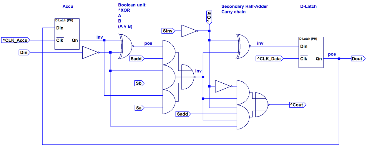

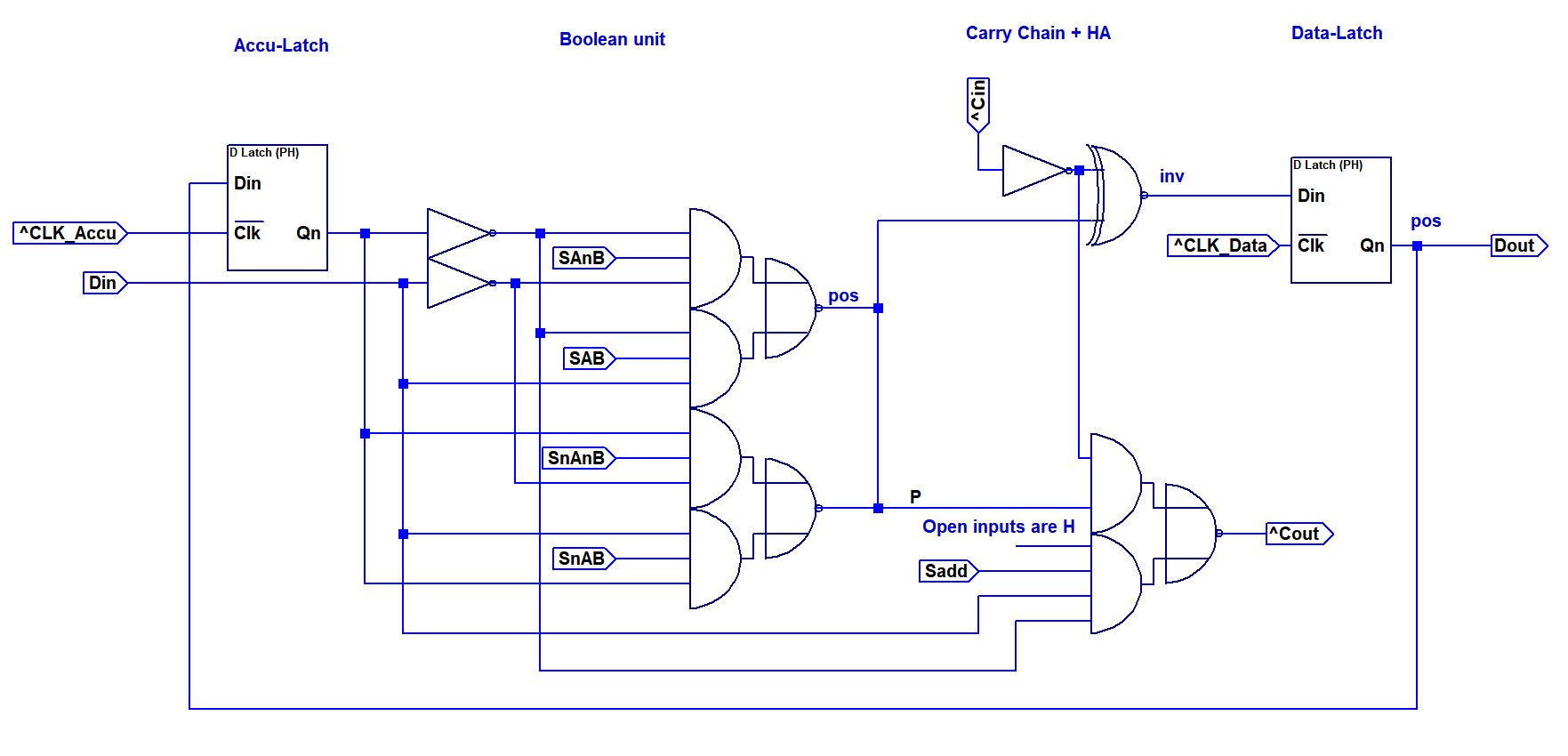
The second option I looked into is a bit more universial and uses an AND-OR-INVERTER based multiplexer for the first stage of the ALU. (EDIT: 20/03/28, updated to fixed version.) By using the four control signals, it is possible to generate any boolean functions, offering the possibility to extend the instruction set of the CPU at a later time. This design is, of course, heavily inspried from the MT-15 ALU. Since the first stage is now also able to implement NOR, it was possible to remove the Sinv control signal. Instead only Sadd is present, which will inhibit carry generation if set to 0.
 Component requirements are shown in the table above. The total number of components is 82, only two more than the less versalite first option. Therefore I elected to go with this option, since it allows more flexibility.
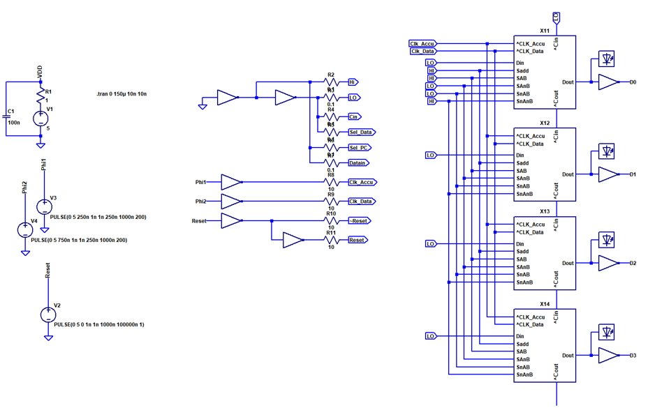
The design functionality was tested in the test bench above.
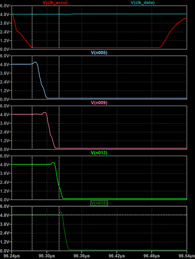 The image above shows carry propagation through all stages. The carry is low active. The carry propagation delay is approximately 11 ns per stage (45 ns total for 4 stages). Although this will propably increase in the real circuit due to more parasitics, it is a very reasonable result and suggests that an acceptably high clockspeed can be achieved even without resorting to a more elaborate carry chain architecture.
 Tim
Tim
Discussions
Become a Hackaday.io Member
Create an account to leave a comment. Already have an account? Log In.